

Datasheet MC68HC705P9S, MC68HC705P9VDW, MC68HC705P9VP, MC68HC705P9MS, MC68HC705P9CS Datasheet (Motorola)
...Page 1

MC68HC705P9/D
REV. 3
MC68HC705P9
HCMOS Microcontroller Unit
TECHNICAL DATA
Page 2

M O T O R O L A
CSIC
MICROCONTROLLERS
Page 3

List of Sections
Table of Contents . . . . . . . . . . . . . . . . . . . . . . . . . 5
Introduction . . . . . . . . . . . . . . . . . . . . . . . . . . . . . . 9
Pin Descriptions . . . . . . . . . . . . . . . . . . . . . . . . . . 13
Memory . . . . . . . . . . . . . . . . . . . . . . . . . . . . . . . . 19
Central Processor Unit (CPU) . . . . . . . . . . . . . . . 33
Resets and Interrupts. . . . . . . . . . . . . . . . . . . . . . 55
Low-Power Modes. . . . . . . . . . . . . . . . . . . . . . . . 65
Parallel I/O Ports . . . . . . . . . . . . . . . . . . . . . . . . . 71
Computer Operating Properly
Watchdog (COP) . . . . . . . . . . . . . . . . . . . . . . 85
Timer. . . . . . . . . . . . . . . . . . . . . . . . . . . . . . . . . . . 89
Serial Input/Output Port (SIOP). . . . . . . . . . . . . 107
Analog-to-Digital Converter (ADC). . . . . . . . . 121
Specifications . . . . . . . . . . . . . . . . . . . . . . . . . . 131
Index . . . . . . . . . . . . . . . . . . . . . . . . . . . . . . . . . 145
Literature Updates. . . . . . . . . . . . . . . . . . . . . . . 151
Motorola, Inc., 1996
MOTOROLA 3
Page 4

List of Sections
List of Modules
List of Modules
All M68HC05 microcontroller units (MCUs) are customer-specified
modular designs. To meet customer requirements, Motorola is
constantly designing new modules and new versions of existing
modules. The following table shows the version levels of the modules in
the MC68HC705P9 MCU.
Module Version
Central Processor Unit (CPU) HC05CPU
Timer TIM1IC1OC_A
Serial Input/Output Port (SIOP) SIOP_A
Computer Operating Properly Watchdog (COP) COP0COP
Analog-to-Digital Converter (ADC) ATD4X8NVRL
Revision History
The following table summarizes differences between this revision and
the previous revision of this Technical Data manual.
Previous
Revision
Current
Revision
Date 11/95
Changes Format and organizational changes
Location Throughout
2.0
3.0
4 MOTOROLA
Page 5

Table of Contents
List of Sections List of Modules . . . . . . . . . . . . . . . . . . . . . . . . . . . . . . . . . . . . . . . . . . .4
Revision History. . . . . . . . . . . . . . . . . . . . . . . . . . . . . . . . . . . . . . . . . . .4
Introduction Contents . . . . . . . . . . . . . . . . . . . . . . . . . . . . . . . . . . . . . . . . . . . . . . . .9
Features . . . . . . . . . . . . . . . . . . . . . . . . . . . . . . . . . . . . . . . . . . . . . . .10
Structure . . . . . . . . . . . . . . . . . . . . . . . . . . . . . . . . . . . . . . . . . . . . . . .11
Package Types and Order Numbers. . . . . . . . . . . . . . . . . . . . . . . . . .12
Programmable Options . . . . . . . . . . . . . . . . . . . . . . . . . . . . . . . . . . . .12
Pin Descriptions Contents . . . . . . . . . . . . . . . . . . . . . . . . . . . . . . . . . . . . . . . . . . . . . . .13
Pin Assignments . . . . . . . . . . . . . . . . . . . . . . . . . . . . . . . . . . . . . . . . .14
Pin Functions. . . . . . . . . . . . . . . . . . . . . . . . . . . . . . . . . . . . . . . . . . . .15
Memory Contents . . . . . . . . . . . . . . . . . . . . . . . . . . . . . . . . . . . . . . . . . . . . . . .19
Features . . . . . . . . . . . . . . . . . . . . . . . . . . . . . . . . . . . . . . . . . . . . . . .19
Memory Map . . . . . . . . . . . . . . . . . . . . . . . . . . . . . . . . . . . . . . . . . . . .20
Input/Output Register Summary . . . . . . . . . . . . . . . . . . . . . . . . . . . . .21
RAM. . . . . . . . . . . . . . . . . . . . . . . . . . . . . . . . . . . . . . . . . . . . . . . . . . .24
EPROM/OTPROM. . . . . . . . . . . . . . . . . . . . . . . . . . . . . . . . . . . . . . . . . . . . . . . . . .25
Mask Option Register . . . . . . . . . . . . . . . . . . . . . . . . . . . . . . . . . . . . .31
CPU Contents . . . . . . . . . . . . . . . . . . . . . . . . . . . . . . . . . . . . . . . . . . . . . . .33
Features . . . . . . . . . . . . . . . . . . . . . . . . . . . . . . . . . . . . . . . . . . . . . . .34
Introduction . . . . . . . . . . . . . . . . . . . . . . . . . . . . . . . . . . . . . . . . . . . . .34
MOTOROLA Table of Contents 5
Page 6

Table of Contents
CPU Control Unit. . . . . . . . . . . . . . . . . . . . . . . . . . . . . . . . . . . . . . . . .36
Arithmetic/Logic Unit . . . . . . . . . . . . . . . . . . . . . . . . . . . . . . . . . . . . . .36
CPU Registers. . . . . . . . . . . . . . . . . . . . . . . . . . . . . . . . . . . . . . . . . . .36
Instruction Set . . . . . . . . . . . . . . . . . . . . . . . . . . . . . . . . . . . . . . . . . . .40
Resets and
Interrupts
Low-Power Modes Contents . . . . . . . . . . . . . . . . . . . . . . . . . . . . . . . . . . . . . . . . . . . . . . .65
Parallel I/O Ports Contents . . . . . . . . . . . . . . . . . . . . . . . . . . . . . . . . . . . . . . . . . . . . . . .71
Contents . . . . . . . . . . . . . . . . . . . . . . . . . . . . . . . . . . . . . . . . . . . . . . .55
Resets . . . . . . . . . . . . . . . . . . . . . . . . . . . . . . . . . . . . . . . . . . . . . . . . .56
Low-Voltage Protection . . . . . . . . . . . . . . . . . . . . . . . . . . . . . . . . . . . .58
Interrupts . . . . . . . . . . . . . . . . . . . . . . . . . . . . . . . . . . . . . . . . . . . . . . .59
Stop Mode. . . . . . . . . . . . . . . . . . . . . . . . . . . . . . . . . . . . . . . . . . . . . .65
Wait Mode . . . . . . . . . . . . . . . . . . . . . . . . . . . . . . . . . . . . . . . . . . . . . .68
Data-Retention Mode . . . . . . . . . . . . . . . . . . . . . . . . . . . . . . . . . . . . .70
Introduction . . . . . . . . . . . . . . . . . . . . . . . . . . . . . . . . . . . . . . . . . . . . .72
Port A. . . . . . . . . . . . . . . . . . . . . . . . . . . . . . . . . . . . . . . . . . . . . . . . . .73
Port B. . . . . . . . . . . . . . . . . . . . . . . . . . . . . . . . . . . . . . . . . . . . . . . . . .76
Port C . . . . . . . . . . . . . . . . . . . . . . . . . . . . . . . . . . . . . . . . . . . . . . . . .79
Port D . . . . . . . . . . . . . . . . . . . . . . . . . . . . . . . . . . . . . . . . . . . . . . . . .82
COP Contents . . . . . . . . . . . . . . . . . . . . . . . . . . . . . . . . . . . . . . . . . . . . . . .85
Features . . . . . . . . . . . . . . . . . . . . . . . . . . . . . . . . . . . . . . . . . . . . . . .85
Introduction . . . . . . . . . . . . . . . . . . . . . . . . . . . . . . . . . . . . . . . . . . . . .86
Operation. . . . . . . . . . . . . . . . . . . . . . . . . . . . . . . . . . . . . . . . . . . . . . .86
Interrupts . . . . . . . . . . . . . . . . . . . . . . . . . . . . . . . . . . . . . . . . . . . . . . .87
COP Register . . . . . . . . . . . . . . . . . . . . . . . . . . . . . . . . . . . . . . . . . . .87
Low-Power Modes. . . . . . . . . . . . . . . . . . . . . . . . . . . . . . . . . . . . . . . .88
6 Table of Contents MOTOROLA
Page 7

Table of Contents
Timer Contents . . . . . . . . . . . . . . . . . . . . . . . . . . . . . . . . . . . . . . . . . . . . . . .89
Features . . . . . . . . . . . . . . . . . . . . . . . . . . . . . . . . . . . . . . . . . . . . . . .90
Introduction . . . . . . . . . . . . . . . . . . . . . . . . . . . . . . . . . . . . . . . . . . . . .90
Operation. . . . . . . . . . . . . . . . . . . . . . . . . . . . . . . . . . . . . . . . . . . . . . .93
Timing . . . . . . . . . . . . . . . . . . . . . . . . . . . . . . . . . . . . . . . . . . . . . . . . .95
Interrupts . . . . . . . . . . . . . . . . . . . . . . . . . . . . . . . . . . . . . . . . . . . . . . .98
I/O Registers . . . . . . . . . . . . . . . . . . . . . . . . . . . . . . . . . . . . . . . . . . . .98
Low-Power Modes. . . . . . . . . . . . . . . . . . . . . . . . . . . . . . . . . . . . . . .106
SIOP Contents . . . . . . . . . . . . . . . . . . . . . . . . . . . . . . . . . . . . . . . . . . . . . .107
Features . . . . . . . . . . . . . . . . . . . . . . . . . . . . . . . . . . . . . . . . . . . . . .108
Introduction . . . . . . . . . . . . . . . . . . . . . . . . . . . . . . . . . . . . . . . . . . . .108
Operation. . . . . . . . . . . . . . . . . . . . . . . . . . . . . . . . . . . . . . . . . . . . . .110
Timing . . . . . . . . . . . . . . . . . . . . . . . . . . . . . . . . . . . . . . . . . . . . . . . .114
Interrupts . . . . . . . . . . . . . . . . . . . . . . . . . . . . . . . . . . . . . . . . . . . . . .115
I/O Registers . . . . . . . . . . . . . . . . . . . . . . . . . . . . . . . . . . . . . . . . . . .116
Low-Power Modes. . . . . . . . . . . . . . . . . . . . . . . . . . . . . . . . . . . . . . .120
ADC Contents . . . . . . . . . . . . . . . . . . . . . . . . . . . . . . . . . . . . . . . . . . . . . .121
Features . . . . . . . . . . . . . . . . . . . . . . . . . . . . . . . . . . . . . . . . . . . . . .121
Introduction . . . . . . . . . . . . . . . . . . . . . . . . . . . . . . . . . . . . . . . . . . . .122
Operation. . . . . . . . . . . . . . . . . . . . . . . . . . . . . . . . . . . . . . . . . . . . . .123
Interrupts . . . . . . . . . . . . . . . . . . . . . . . . . . . . . . . . . . . . . . . . . . . . . .124
Timing and Electrical Characteristics . . . . . . . . . . . . . . . . . . . . . . . .125
I/O Registers . . . . . . . . . . . . . . . . . . . . . . . . . . . . . . . . . . . . . . . . . . .126
Low-Power Modes. . . . . . . . . . . . . . . . . . . . . . . . . . . . . . . . . . . . . . .130
MOTOROLA Table of Contents 7
Page 8

Table of Contents
Specifications Contents . . . . . . . . . . . . . . . . . . . . . . . . . . . . . . . . . . . . . . . . . . . . . .131
Maximum Ratings . . . . . . . . . . . . . . . . . . . . . . . . . . . . . . . . . . . . . . .132
Operating Temperature Range . . . . . . . . . . . . . . . . . . . . . . . . . . . . .133
Thermal Characteristics. . . . . . . . . . . . . . . . . . . . . . . . . . . . . . . . . . .133
Power Considerations . . . . . . . . . . . . . . . . . . . . . . . . . . . . . . . . . . . .134
5.0 V DC Electrical Characteristics . . . . . . . . . . . . . . . . . . . . . . . . . .135
3.3 V DC Electrical Characteristics . . . . . . . . . . . . . . . . . . . . . . . . . .136
Driver Characteristics . . . . . . . . . . . . . . . . . . . . . . . . . . . . . . . . . . . .137
Typical Supply Current vs. Internal Clock Frequency . . . . . . . . . . . .138
Maximum Supply Current vs. Internal Clock Frequency . . . . . . . . . .139
5.0 V Control Timing . . . . . . . . . . . . . . . . . . . . . . . . . . . . . . . . . . . . .140
3.3 V Control Timing . . . . . . . . . . . . . . . . . . . . . . . . . . . . . . . . . . . . .141
Test Load. . . . . . . . . . . . . . . . . . . . . . . . . . . . . . . . . . . . . . . . . . . . . .142
Mechanical Specifications. . . . . . . . . . . . . . . . . . . . . . . . . . . . . . . . .142
Index . . . . . . . . . . . . . . . . . . . . . . . . . . . . . . . . . . . . . . . . . . . . . . . . . . . . . .145
Literature Updates Literature Distribution Centers. . . . . . . . . . . . . . . . . . . . . . . . . . . . . .151
Mfax. . . . . . . . . . . . . . . . . . . . . . . . . . . . . . . . . . . . . . . . . . . . . . . . . .152
Motorola SPS World Marketing World Wide Web Server . . . . . . . . .152
CSIC Microcontroller Division’s Web Site . . . . . . . . . . . . . . . . . . . . .152
8 Table of Contents MOTOROLA
Page 9

Contents
Introduction
Features . . . . . . . . . . . . . . . . . . . . . . . . . . . . . . . . . . . . . . . . . . . . . . .10
Structure . . . . . . . . . . . . . . . . . . . . . . . . . . . . . . . . . . . . . . . . . . . . . . .11
Package Types and Order Numbers. . . . . . . . . . . . . . . . . . . . . . . . . .12
Programmable Options . . . . . . . . . . . . . . . . . . . . . . . . . . . . . . . . . . . .12
1-mc68hc705p9
MOTOROLA Introduction 9
Page 10

Features
Introduction
• Four Peripheral Modules
• 20 Bidirectional I/O Port Pins and One Input-Only Port Pin
• On-Chip Oscillator with Connections for:
• 2104 Bytes of EPROM/OTPROM
Features
– 16-Bit Input Capture/Output Compare Timer
– Synchronous Serial I/O Port (SIOP)
– 4-Channel, 8-Bit Analog-to-Digital Converter (ADC)
– Computer Operating Properly (COP) Watchdog
– Crystal
– Ceramic Resonator
– External Clock
– 48 Bytes of Page Zero EPROM/OTPROM
– Eight Locations for User Vectors
• 128 Bytes of User RAM
• Bootloader ROM
• Memory-Mapped Input/Output (I/O) Registers
• Fully Static Operation with No Minimum Clock Speed
• Power-Saving Stop, Wait, and Data-Retention Modes
2-mc68hc705p9
10 Introduction MOTOROLA
Page 11
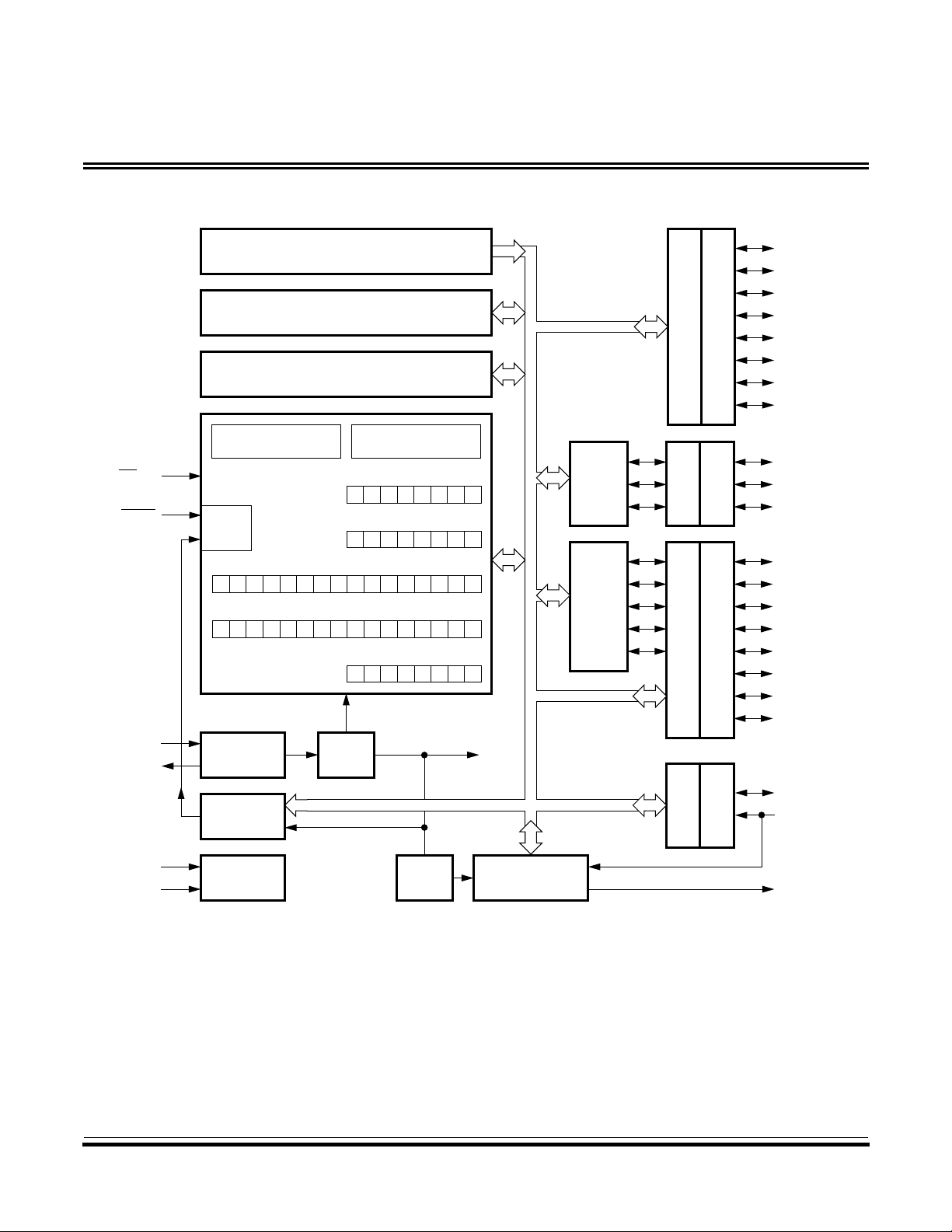
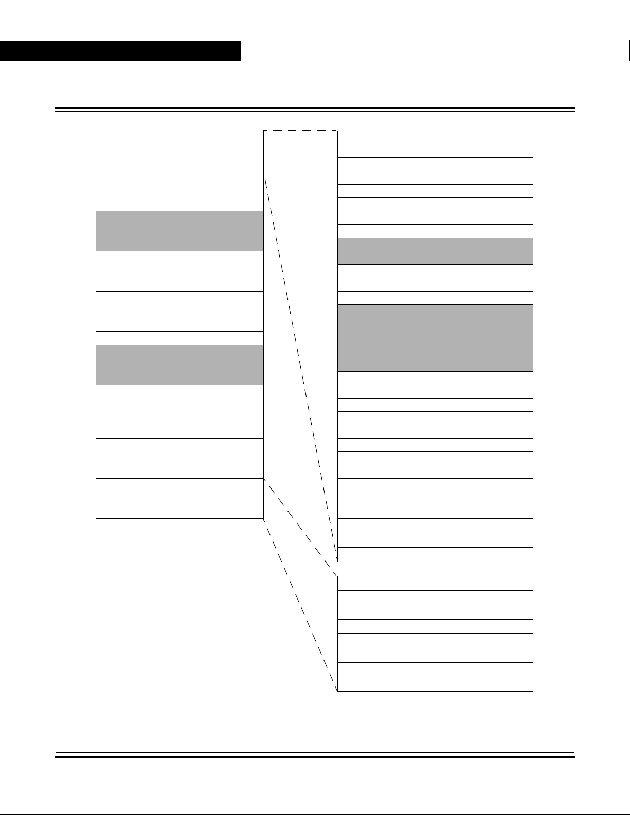
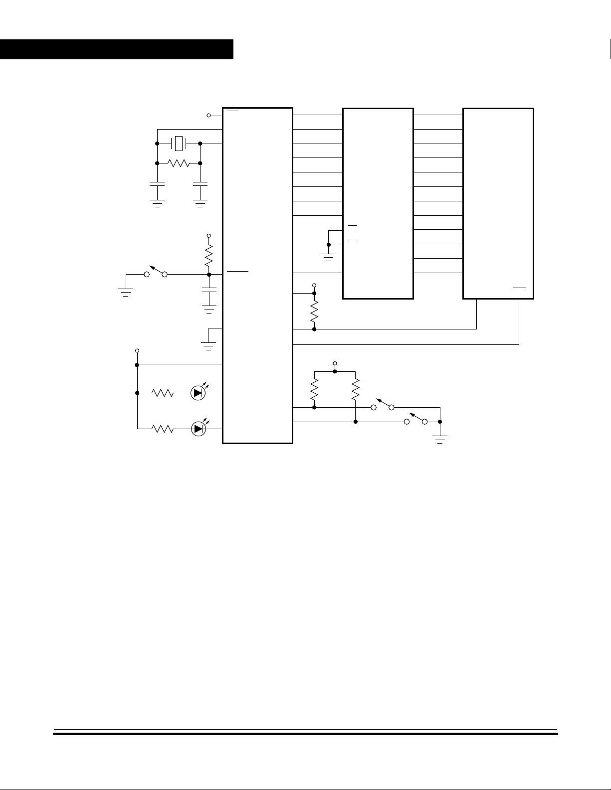
Structure
Introduction
Structure
IRQ/V
RESET
OSC1
OSC2
EPROM/OTPROM — 2104 BYTES
BOOTLOADER ROM — 240 BYTES
PORT A
RAM — 128 BYTES
DATA DIRECTION REGISTER A
CPU CONTROL
PP
RESET
00
INTERNAL
OSCILLATOR
M68HC05
MCU
STACK POINTER
0000011
000
PROGRAM COUNTER
0
ARITHMETIC/LOGIC
UNIT
ACCUMULATOR
INDEX REGISTER
CONDITION CODE REGISTER
111HINCZ
CPU CLOCK
DIVIDE
INTERNAL CLOCK
BY 2
TO ADC
AND
SIOP
SIOP
ADC
SCK
SDI
SDO
V
AN0
AN1
AN2
AN3
PORT B
REGISTER B
DA TA DIRECTION
RH
PORT C
DATA DIRECTION REGISTER C
PA7
PA6
PA5
PA4
PA3
PA2
PA1
PA0
PB7/SCK
PB6/SDI
PB5/SDO
PC7/V
RH
PC6/AN0
PC5/AN1
PC4/AN2
PC3/AN3
PC2
PC1
PC0
PD5
COP
WATCHDOG
V
DD
V
SS
POWER
DIVIDE
BY 4
CAPTURE/COMPARE
TIMER
TCAP
PORT D
REGISTER D
DA TA DIRECTION
PD7/TCAP
TCMP
Figure 1. MC68HC705P9 Block Diagram
3-mc68hc705p9
MOTOROLA Introduction 11
Page 12

Introduction
Package Types and Order Numbers
Package Types and Order Numbers
Table 1. Order Numbers
Package
Plastic DIP
SOIC
CERDIP
1. DIP = dual in-line package
2. SOIC = small outline integrated circuit
3. CERDIP = ceramic DIP
Programmable Options
Type
(2)
(3)
(1)
Case
Outline
710 28
733 28
751F 28
Count
Pin
Operating
Temperature
0 to +70 °C
–40 to +85 °C
–40 to +105 °C
–40 to +125 °C
0 to +70 °C
–40 to +85 °C
–40 to +105 °C
–40 to +125 °C
0 to +70 °C
–40 to +85 °C
–40 to +105 °C
–40 to +125 °C
Order Number
MC68HC705P9P
MC68HC705P9CP
MC68HC705P9VP
MC68HC705P9MP
MC68HC705P9DW
MC68HC705P9CDW
MC68HC705P9VDW
MC68HC705P9MDW
MC68HC705P9S
MC68HC705P9CS
MC68HC705P9VS
MC68HC705P9MS
The options in Table 2 are programmable in the mask option register.
Table 2. Programmable Options
Feature Option
Enabled
COP Watchdog
External Interrupt Pin Triggering
SIOP Data Format
12 Introduction MOTOROLA
or
Disabled
Negative-Edge Triggering Only
or
Negative-Edge and Low-Level Triggering
MSB First
or
LSB First
4-mc68hc705p9
Page 13

Contents
Pin Descriptions
Pin Assignments . . . . . . . . . . . . . . . . . . . . . . . . . . . . . . . . . . . . . . . . .14
Pin Functions. . . . . . . . . . . . . . . . . . . . . . . . . . . . . . . . . . . . . . . . . . . .15
V
and VSS. . . . . . . . . . . . . . . . . . . . . . . . . . . . . . . . . . . . . . . . . . .15
DD
OSC1 and OSC2. . . . . . . . . . . . . . . . . . . . . . . . . . . . . . . . . . . . . . .15
Crystal Connections . . . . . . . . . . . . . . . . . . . . . . . . . . . . . . . . . .16
Ceramic Resonator Connections . . . . . . . . . . . . . . . . . . . . . . . .16
External Clock Connections . . . . . . . . . . . . . . . . . . . . . . . . . . . .17
RESET . . . . . . . . . . . . . . . . . . . . . . . . . . . . . . . . . . . . . . . . . . . . . .17
IRQ/VPP. . . . . . . . . . . . . . . . . . . . . . . . . . . . . . . . . . . . . . . . . . . . . .17
PA7–PA0. . . . . . . . . . . . . . . . . . . . . . . . . . . . . . . . . . . . . . . . . . . . .17
PB7/SCK–PB5/SDO . . . . . . . . . . . . . . . . . . . . . . . . . . . . . . . . . . . .17
PC7/V
PD7/TCAP and PD5 . . . . . . . . . . . . . . . . . . . . . . . . . . . . . . . . . . . .18
TCMP . . . . . . . . . . . . . . . . . . . . . . . . . . . . . . . . . . . . . . . . . . . . . . .18
–PC0 . . . . . . . . . . . . . . . . . . . . . . . . . . . . . . . . . . . . . . . . .17
RH
1-mc68hc705p9
MOTOROLA Pin Descriptions 13
Page 14
Pin Descriptions
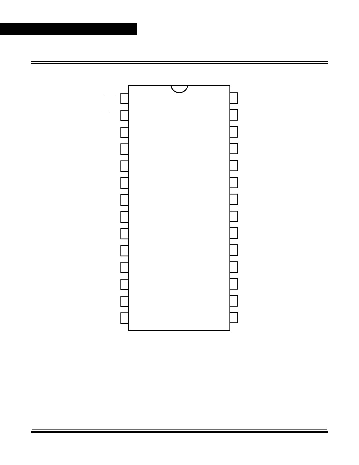
Pin Assignments
Pin Assignments
RESET
IRQ/V
PA7
PA6
PA5
PA4
PA3
PA2
PA1
PA0
PB5/SDO
V
DD
PP
OSC1
OSC2
PD7/TCAP
TCMP
PD5
PC0
PC1
PC2
PC3/AN3
PC4/AN2
PB6/SDI
PB7/SCK
V
SS
PC5/AN1
PC6/AN0
PC7/V
RH
Figure 1. Pin Assignments
2-mc68hc705p9
14 Pin Descriptions MOTOROLA
Page 15
Pin Functions
Pin Descriptions
Pin Functions
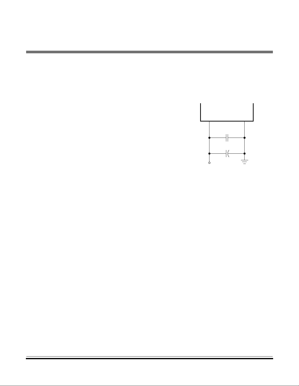
VDD and V
SS
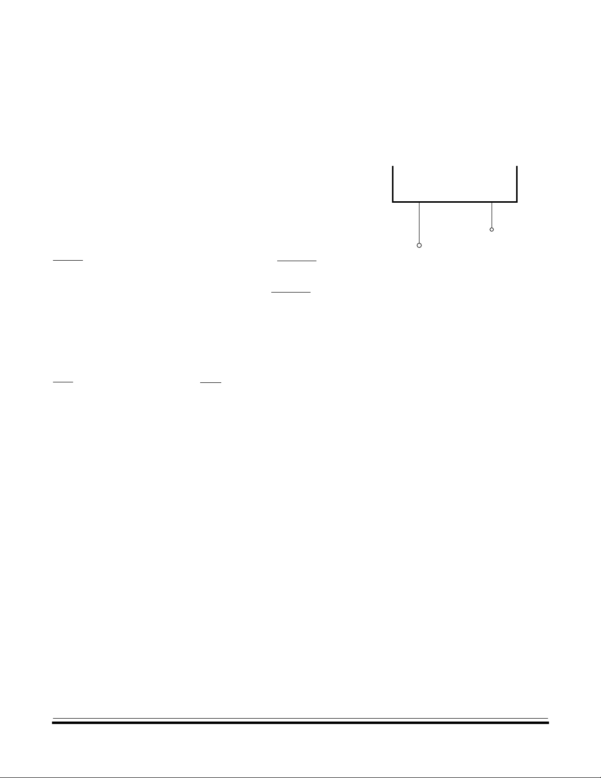
VDD and VSSare the power supply and ground pins. The MCU operates
from a single 5-V power supply.
Very fast signal transitions occur
on the MCU pins, placing high
short-duration current demands
MCU
on the power supply. To prevent
noise problems, take special
care to provide good power
DD
V
C1
0.1 µF
SS
V
supply bypassing at the MCU as
Figure 2 shows. Place the
bypass capacitors as close as
possible to the MCU. C2 is an
V
DD
C2
+
optional bulk current bypass
capacitor for use in applications
that require the port pins to
Figure 2. Bypassing
Recommendation
source high current levels.
OSC1 and OSC2 The OSC1 and OSC2 pins are the connections for the on-chip oscillator.
The oscillator can be driven by any of the following:
• Crystal
• Ceramic resonator
• External clock signal
The frequency of the on-chip oscillator is f
. The MCU divides the
OSC
internal oscillator output by two to produce the internal clock with a
frequency of f
3-mc68hc705p9
OP
.
MOTOROLA Pin Descriptions 15
Page 16
Pin Descriptions
Pin Functions
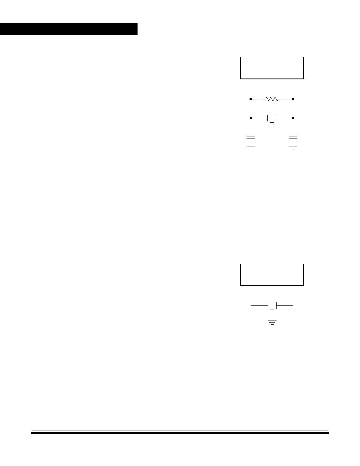
Crystal Connections
NOTE:
The circuit in Figure 3 shows a
typical crystal oscillator circuit
MCU
for an AT-cut, parallel resonant
crystal. Follow the crystal
supplier’s recommendations, as
OSC1
10 MΩ
OSC2
the crystal parameters
determine the external
XTAL
component values required to
provide reliable startup and
maximum stability. The load
27 pF 27 pF
capacitance values used in the
oscillator circuit design should
include all stray layout
Figure 3. Crystal Connections
capacitances. To minimize
output distortion, mount the
crystal and capacitors as close
as possible to the pins.
Use an AT-cut crystal. Do not use a strip or tuning fork crystal. The MCU
may overdrive or have the incorrect characteristic impedance for a strip
or tuning fork crystal.
Ceramic Resonator Connections
To reduce cost, use a ceramic
resonator in place of the crystal.
Figure 4 shows a ceramic
resonator circuit. For the values
of any external components,
follow the recommendations of
the resonator manufacturer. The
load capacitance values used in
the oscillator circuit design
should include all stray layout
capacitances. To minimize
output distortion, mount the
resonator and capacitors as
close as possible to the pins.
MCU
CERAMIC
RESONATOR
OSC1
OSC2
Figure 4. Ceramic Resonator
Connections
4-mc68hc705p9
16 Pin Descriptions MOTOROLA
Page 17
Pin Descriptions
Pin Functions
NOTE:
Because the frequency stability of ceramic resonators is not as high as
that of crystal oscillators, using a ceramic resonator may degrade the
performance of the ADC.
External Clock Connections
An external clock from another
CMOS-compatible device can
drive the OSC1 input, with the
OSC2 pin unconnected, as
Figure 5 shows.
RESET A logic zero on the RESET pin
forces the MCU to a known
startup state. The
RESET pin
input circuit contains an internal
Schmitt trigger to improve noise
immunity.
MCU
OSC1
UNCONNECTED
EXTERNAL
CMOS CLOCK
OSC2
Figure 5. External Clock
Connections
IRQ/V
PP
The IRQ/VPP pin has the following functions:
• Applying asynchronous external interrupt signals
• Applying VPP, the EPROM/OTPROM programming voltage
PA7–PA0 PA7–PA0 are general-purpose bidirectional I/O port pins. Use data
direction register A to configure port A pins as inputs or outputs.
PB7/SCK– PB5/SDO
Port B is a 3-pin bidirectional I/O port that shares its pins with the SIOP.
Use data direction register B to configure port B pins as inputs or
outputs.
PC7/VRH–PC0 Port C is an 8-pin bidirectional I/O port that shares five of its pins with the
ADC. Use data direction register C to configure port C pins as inputs or
outputs.
5-mc68hc705p9
MOTOROLA Pin Descriptions 17
Page 18

Pin Descriptions
Pin Functions
PD7/TCAP and PD5 Port D is a 2-pin I/O port that shares one of its pins with the
capture/compare timer. Use data direction register D to configure port D
pins as inputs or outputs.
TCMP The TCMP pin is the output compare pin for the capture/compare timer.
6-mc68hc705p9
18 Pin Descriptions MOTOROLA
Page 19

Contents
Memory
Features . . . . . . . . . . . . . . . . . . . . . . . . . . . . . . . . . . . . . . . . . . . . . . .19
Memory Map . . . . . . . . . . . . . . . . . . . . . . . . . . . . . . . . . . . . . . . . . . . .20
Input/Output Register Summary . . . . . . . . . . . . . . . . . . . . . . . . . . . . .21
RAM. . . . . . . . . . . . . . . . . . . . . . . . . . . . . . . . . . . . . . . . . . . . . . . . . . .24
EPROM/OTPROM. . . . . . . . . . . . . . . . . . . . . . . . . . . . . . . . . . . . . . . .25
EPROM/OTPROM Programming . . . . . . . . . . . . . . . . . . . . . . . . . .26
EPROM Programming Register . . . . . . . . . . . . . . . . . . . . . . . . .26
Bootloader ROM . . . . . . . . . . . . . . . . . . . . . . . . . . . . . . . . . . . .27
EPROM Erasing . . . . . . . . . . . . . . . . . . . . . . . . . . . . . . . . . . . . . . .30
Mask Option Register . . . . . . . . . . . . . . . . . . . . . . . . . . . . . . . . . . . . .31
Features
1-mc68hc705p9
• 2104 Bytes of EPROM/OTPROM
– 48 Bytes of Page Zero EPROM/OTPROM
– Eight Locations for User Vectors
• 128 Bytes of User RAM
• Bootloader ROM
MOTOROLA Memory 19
Page 20
Memory Map
Memory
Memory Map
$0000
↓
$001F
$0020
↓
$004F
$0050
↓
$007F
$0080
↓
$00FF
$0100
↓
$08FF
$0900 Mask Option Register $000F
$0901
↓
$1EFF
$1F00
↓
$1FEF
$1FF0 COP Control Register Output Compare Register High (OCRH) $0016
$1FF1
↓
$1FF7
$1FF8
↓
$1FFF
I/O Registers (32 Bytes)
Page Zero User EPROM (48 Bytes)
Unimplemented (48 Bytes)
RAM (128 Bytes)
User EPROM (2048 Bytes)
Unimplemented (5631 Bytes)
Bootloader ROM (240 Bytes)
Reserved
User Vector EPROM (8 Bytes)
Port A Data Register (PORTA) $0000
Port B Data Register (PORTB) $0001
Port C Data Register (PORTC) $0002
Port D Data Register (PORTD) $0003
Data Direction Register A (DDRA) $0004
Data Direction Register B (DDRB) $0005
Data Direction Register C (DDRC) $0006
Data Direction Register D (DDRD) $0007
Unimplemented
SIOP Control Register (SCR) $000A
SIOP Status Register (SSR) $000B
SIOP Data Register (SDR) $000C
Unimplemented
Timer Control Register (TCR) $0012
Timer Status Register (TSR) $0013
Input Capture Register High (ICRH) $0014
Input Capture Register Low (ICRL) $0015
Output Compare Register Low (OCRL) $0017
Timer Register High (TRH) $0018
Timer Register Low (TRL) $0019
Alternate Timer Register High (ATRH) $001A
Alternate Timer Register Low (ATRL) $001B
EPROM Programming Register (EPROG) $001C
ADC Data Register (ADDR) $001D
ADC Status/Control Register (ADSCR) $001E
Reserved $001F
$0008
$0009
$000D
$000E
$0010
$0011
Timer Interrupt Vector High $1FF8
Timer Interrupt Vector Low $1FF9
External Interrupt Vector High $1FFA
External Interrupt Vector Low $1FFB
Software Interrupt Vector High $1FFC
Software Interrupt Vector Low $1FFD
Reset Vector High $1FFE
Reset Vector Low $1FFF
Figure 1. Memory Map
2-mc68hc705p9
20 Memory MOTOROLA
Page 21
Memory
Input/Output Register Summary
Input/Output Register Summary
Addr. Name R/W Bit 7 654321Bit 0
$0000
Port A Data Register (PORTA)
Read:
Write:
Reset:
PA7 PA6 PA5 PA4 PA3 PA2 PA1 PA0
Unaffected by reset
$0001
$0002
$0003
$0004
$0005
$0006
Port B Data Register (PORTB)
Port C Data Register (PORTC)
Port D Data Register (PORTD)
Data Direction Register A (DDRA)
Data Direction Register B (DDRB)
Data Direction Register C (DDRC)
Read:
Write:
PB7 PB6 PB5
Reset:
Read:
Write:
PC7 PC6 PC5 PC4 PC3 PC2 PC1 PC0
Reset:
Read:
Write:
PD7
0
PD5
Reset:
Read:
DDRA7 DDRA6 DDRA5 DDRA4 DDRA3 DDRA2 DDRA1 DDRA0
Write:
Reset:
Read:
Write:
Reset:
Read:
Write:
Reset:
00000000
DDRB7 DDRB6 DDRB5
00000000
DDRC7 DDRC6 DDRC5 DDRC4 DDRC3 DDRC2 DDRC1 DDRC0
00000000
00000
Unaffected by reset
Unaffected by reset
10000
Unaffected by reset
00000
$0007
$0008
$0009
Data Direction Register D (DDRD)
Unimplemented
Unimplemented
Read:
Write:
Reset:
00
00000000
= Unimplemented
DDRD5
00000
= Reserved U = Unaffected
R
Figure 2. I/O Register Summary
3-mc68hc705p9
MOTOROLA Memory 21
Page 22
Memory
Input/Output Register Summary
Addr. Name R/W Bit 7 654321Bit 0
$000A
SIOP Control Register (SCR)
Read:
Write:
Reset:
0 SPE 0 MSTR 0000
00000000
$000B
$000C
$000D
$000E
$000F
$0010
$0011
$0012
$0013
SIOP Status Register (SSR)
SIOP Data Register (SDR)
Unimplemented
Unimplemented
Unimplemented
Unimplemented
Unimplemented
Timer Control Register (TCR)
Timer Status Register (TSR)
Read:
Write:
Reset:
Read:
Write:
Reset:
Read:
Write:
Reset:
Read:
Write:
Reset:
SPIF DCOL 000000
00000000
Bit 7 654321Bit 0
Unaffected by reset
ICIE OCIE TOIE 0 0 0 IEDG OLVL
000000U0
ICFOCFTOF00000
Unaffected by reset 00000
$0014
Input Capture Register High (ICRH)
Read:
Write:
Bit 15 14 13 12 11 10 9 Bit 8
Reset:
$0015
$0016
Input Capture Register Low (ICRL)
Output Compare Register High (OCRH)
Read:
Write:
Reset:
Read:
Write:
Reset:
Bit 7 654321Bit 0
Unaffected by reset
Bit 15 14 13 12 11 10 9 Bit 8
Unaffected by reset
= Unimplemented
= Reserved U = Unaffected
R
Figure 2. I/O Register Summary (Continued)
4-mc68hc705p9
22 Memory MOTOROLA
Page 23
Memory
Input/Output Register Summary
Addr. Name R/W Bit 7 654321Bit 0
$0017
Output Compare Register Low (OCRL)
Read:
Write:
Reset:
Bit 7 654321Bit 0
Unaffected by reset
$0018
$0019
$001A
$001B
$001C
$001D
Timer Register High (TRH)
Timer Register Low (TRL)
Alternate Timer Register High (ATRH)
Alternate Timer Register Low (ATRL)
EPROMProgramming Register (EPROG)
ADC Data Register (ADDR)
Read:
Write:
Reset:
Read:
Write:
Reset:
Read:
Write:
Reset:
Read:
Write:
Reset:
Read:
Write:
Reset:
Read:
Write:
Reset:
Bit 15 14 13 12 11 10 9 Bit 8
Reset initializes TRH to $FF
Bit 7 654321Bit 0
Reset initializes TRL to $FC
Bit 15 14 13 12 11 10 9 Bit 8
Reset initializes ATRH to $FF
Bit 7 654321Bit 0
Reset initializes ATRL to $FC
00000
RRRRR R
Unaffected by reset
Bit 7 654321Bit 0
Unaffected by reset
LATCH
0
EPGM
$001E
$001F
ADC Status/Control Register (ADSCR)
Reserved
Read:
Write:
Reset:
Read:
Write:
CCF
ADRC ADON
00000000
RRRRRRRR
00
CH2 CH1 CH0
Reset:
= Unimplemented
= Reserved U = Unaffected
R
Figure 2. I/O Register Summary (Continued)
5-mc68hc705p9
MOTOROLA Memory 23
Page 24

Memory
Addr. Name R/W Bit 7 654321Bit 0
RAM
$0900
$1FF0
RAM
Mask Option Register (MOR)
COP Register (COPR)
Figure 2. I/O Register Summary (Continued)
The 128 addresses from $0080–$00FF are RAM locations. The CPU
uses the top 64 RAM addresses, $00C0–$00FF, as the stack. Before
processing an interrupt, the CPU uses five bytes of the stack to save the
contents of the CPU registers. During a subroutine call, the CPU uses
two bytes of the stack to store the return address. The stack pointer
decrements when the CPU stores a byte on the stack and increments
when the CPU retrieves a byte from the stack.
Read:
Write:
Reset:
Read:
Write:
Reset:
00000SIOP IRQ COPE
Unaffected by reset 0
RRRRRRRCOPC
Unaffected by reset
= Unimplemented
= Reserved U = Unaffected
R
NOTE:
Be careful when using nested subroutines or multiple interrupt levels.
The CPU may overwrite data in the RAM during a subroutine or during
the interrupt stacking operation.
6-mc68hc705p9
24 Memory MOTOROLA
Page 25

EPROM/OTPROM
Memory
EPROM/OTPROM
An MCU with a quartz window has 2104 bytes of erasable,
programmable ROM (EPROM). The quartz window allows EPROM
erasure with ultraviolet light.
NOTE:
Keep the quartz window covered with an opaque material except when
programming the MCU. Ambient light may affect MCU operation.
In an MCU without the quartz window, the EPROM cannot be erased
and serves as 2104 bytes of one-time programmable ROM (OTPROM).
The following addresses are user EPROM/OTPROM locations:
• $0020–$004F
• $0100–$08FF
• $1FF8–$1FFF (reserved for user-defined interrupt and reset
vectors)
The mask option register (MOR) is an EPROM/OTPROM location at
address $0900.
7-mc68hc705p9
MOTOROLA Memory 25
Page 26

Memory
EPROM/OTPROM
EPROM/ OTPROM Programming
EPROM Programming Register
The two ways to program the EPROM/OTPROM are:
• Manipulating the control bits in the EPROM programming register
to program the EPROM/OTPROM on a byte-by-byte basis
• Activating the bootloader ROM to download the contents of an
external memory device to the on-chip EPROM/OTPROM
The EPROM programming register contains the control bits for
programming the EPROM/OTPROM.
$001C Bit 7 654321Bit 0
Read: 00000
LATCH
Write: RRRRR R
Reset: 00000000
R = Reserved
0
EPGM
Figure 3. EPROM Programming Register (EPROG)
LATCH — EPROM Bus Latch
This read/write bit latches the address and data buses for
EPROM/OTPROM programming. Clearing the LATCH bit
automatically clears the EPGM bit. EPROM/OTPROM data cannot be
read while the LATCH bit is set. Resets clear the LATCH bit.
1 = Address and data buses configured for EPROM/OTPROM
programming
0 = Address and data buses configured for normal operation
EPGM bit— EPROM Programming
This read/write bit applies the voltage from the
IRQ/VPP pin to the
EPROM/OTPROM. To write the EPGM bit, the LATCH bit must
already be set. Clearing the LATCH bit also clears the EPGM bit.
Resets clear the EPGM bit.
1 = EPROM/OTPROM programming power switched on
0 = EPROM/OTPROM programming power switched off
8-mc68hc705p9
26 Memory MOTOROLA
Page 27

Memory
EPROM/OTPROM
NOTE:
Writing logic ones to both the LATCH and EPGM bits with a single
instruction sets LATCH and clears EPGM. LATCH must be set first by a
separate instruction.
Bits 7–3 and Bit 1— Reserved
Bits 7–3 and bit 1 are factory test bits that always read as logic zeros.
Take the following steps to program a byte of EPROM/OTPROM:
1. Apply 16.5 V to the
IRQ/VPP pin.
2. Set the LATCH bit.
3. Write to any EPROM/OTPROM address.
4. Set the EPGM bit for a time, t
, to apply the programming
EPGM
voltage.
5. Clear the LATCH bit.
Bootloader ROM The bootloader ROM, located at addresses $1F00–$1FEF, contains
routines for copying an external EPROM to the on-chip
EPROM/OTPROM.
The bootloader copies to the following EPROM/OTPROM addresses:
• $0020–$004F
• $0100–$0900
• $1FF0–$1FFF
The addresses of the code in the external EPROM must match the
MC68HC705P9 addresses. The bootloader ignores all other addresses.
Figure 4 shows the circuit for downloading to the on-chip
EPROM/OTPROM from a 2764 EPROM. The bootloader circuit includes
an external 12-bit counter to address the external EPROM. Operation is
fastest when unused external EPROM addresses contain $00. The
bootloader function begins when a rising edge occurs on the
while the V
voltage is on the IRQ/VPP pin, and the PD7/TCAP pin is at
PP
RESETpin
logic one.
9-mc68hc705p9
MOTOROLA Memory 27
Page 28
Memory
EPROM/OTPROM
MC14040B
Q1
Q2
Q3
Q4
Q5
Q6
Q7
Q8
Q9
Q10
Q11
Q12
RST CLK
S1
2 MHz
10 MΩ
10 kΩ
1 µF
D0
D1
D2
D3
D4
D5
D6
D7
CE
OE
2764
A0
A1
A2
A3
A4
A5
A6
A7
A8
A9
MC68HC705P9
2
V
IRQ/V
PP
27
26
V
DD
PP
OSC1
OSC2
PA0
PA1
PA2
PA3
PA4
PA5
PA6
PA7
10
9
8
7
6
5
4
3
A10
1
RESET
PB5
PD7
11
25
A12
V
DD
A11
10 kΩ
17
PC5/AN1
V
DD
16
PC6/AN0
PC1
PC2
21
20
V
DD
PROGRAM
330 Ω
VERIFY
13
12
PB7/SCK
PB6/SDI
PC4
PC3
10 kΩ
18
19
10 kΩ
S2
S3
330 Ω
Figure 4. Bootloader Circuit
10-mc68hc705p9
28 Memory MOTOROLA
Page 29

EPROM/OTPROM
The logical states of the PC4/AN2 and PC3/AN3 pins select the
bootloader function, as Table 1 shows.
Table 1. Bootloader Function Selection
Memory
PC4/AN2 PC3/AN3
1 1 Program and Verify
1 0 Verify Only
Function
Complete the following steps to bootload the MCU:
1. Turn off all power to the circuit.
2. Install the EPROM containing the code to be downloaded.
3. Install the MCU.
4. Select the bootloader function:
a. Open switches S2 and S3 to select the program and verify
function.
b. Open only switch S2 to select only the verify function.
5. Close switch S1.
6. Turn on the V
power supply.
DD
CAUTION:
Turn on the VDD power supply before turning on the VPP power supply.
7. Turn on the VPP power supply.
8. Open switch S1. The bootloader code begins to execute. If the
PROGRAM function is selected, the PROGRAM LED turns on
during programming. If the VERIFY function is selected, the
VERIFY LED turns on when verification is successful. The
PROGRAM and VERIFY functions take about 10 seconds.
9. Close switch S1.
10. Turn off the V
11-mc68hc705p9
MOTOROLA Memory 29
power supply.
PP
Page 30

Memory
EPROM/OTPROM
CAUTION:
Turn off the VPP power supply before turning off the VDD power supply.
11. Turn off the VDD power supply.
EPROM Erasing The erased state of an EPROM bit is zero. Erase the EPROM by
exposing it to 15 Ws/cm
2
of ultraviolet light with a wavelength of 2537
angstroms. Position the ultraviolet light source one inch from the
EPROM. Do not use a shortwave filter.
Cerdip packages have a transparent window for erasing the EPROM
with ultraviolet light. In the windowless PDIP and SOIC packages, the
2104 EPROM bytes function as one-time programmable ROM
(OTPROM).
12-mc68hc705p9
30 Memory MOTOROLA
Page 31

Mask Option Register
The mask option register (MOR) is an EPROM/OTPROM byte that is
programmable only with the bootloader function. The MOR controls the
following options:
To program the MOR, use the 5-step procedure given in the section
EPROM Programming Register on page 26. Write to address $0900 in
step 3.
$0900 Bit 7 654321Bit 0
Memory
Mask Option Register
• LSB first or MSB first SIOP data transfer
• Edge-triggered or edge- and level-triggered external interrupt pin
• Enabled or disabled COP watchdog
Read: 00000SIOP IRQ COPE
Write:
Reset: Unaffected by reset
Erased: 00000000
= Unimplemented
Figure 5. Mask Option Register (MOR)
SIOP — Serial I/O Port
The SIOP bit controls the shift direction into and out of the SIOP shift
register.
1 = SIOP data transferred LSB first (bit 0 first)
0 = SIOP data transferred MSB first (bit 7 first)
IRQ — Interrupt Request
The IRQ bit makes the external interrupt function of the
IRQ/VPP pin
level-triggered as well as edge-triggered.
1 = IRQ/VPP pin negative-edge triggered and low-level triggered
IRQ/VPP pin negative-edge triggered only
0 =
13-mc68hc705p9
MOTOROLA Memory 31
Page 32

Memory
Mask Option Register
COPE — COP Enable
COPE enables the COP watchdog. In applications that have wait
cycles longer than the COP watchdog timeout period, the COP
watchdog can be disabled by not programming the COPE bit to logic
one.
1 = COP watchdog enabled
0 = COP watchdog disabled
14-mc68hc705p9
32 Memory MOTOROLA
Page 33

Contents
Central Processor Unit
CPU
Features . . . . . . . . . . . . . . . . . . . . . . . . . . . . . . . . . . . . . . . . . . . . . . .34
Introduction . . . . . . . . . . . . . . . . . . . . . . . . . . . . . . . . . . . . . . . . . . . . .34
CPU Control Unit. . . . . . . . . . . . . . . . . . . . . . . . . . . . . . . . . . . . . . . . .36
Arithmetic/Logic Unit . . . . . . . . . . . . . . . . . . . . . . . . . . . . . . . . . . . . . .36
CPU Registers. . . . . . . . . . . . . . . . . . . . . . . . . . . . . . . . . . . . . . . . . . .36
Accumulator . . . . . . . . . . . . . . . . . . . . . . . . . . . . . . . . . . . . . . . . . .37
Index Register . . . . . . . . . . . . . . . . . . . . . . . . . . . . . . . . . . . . . . . .37
Stack Pointer . . . . . . . . . . . . . . . . . . . . . . . . . . . . . . . . . . . . . . . . .37
Program Counter . . . . . . . . . . . . . . . . . . . . . . . . . . . . . . . . . . . . . .38
Condition Code Register . . . . . . . . . . . . . . . . . . . . . . . . . . . . . . . .38
Instruction Set . . . . . . . . . . . . . . . . . . . . . . . . . . . . . . . . . . . . . . . . . . .40
Addressing Modes . . . . . . . . . . . . . . . . . . . . . . . . . . . . . . . . . . . . .40
Inherent . . . . . . . . . . . . . . . . . . . . . . . . . . . . . . . . . . . . . . . . . . .40
Immediate . . . . . . . . . . . . . . . . . . . . . . . . . . . . . . . . . . . . . . . . .40
Direct . . . . . . . . . . . . . . . . . . . . . . . . . . . . . . . . . . . . . . . . . . . . .41
Extended . . . . . . . . . . . . . . . . . . . . . . . . . . . . . . . . . . . . . . . . . .41
Indexed, No Offset . . . . . . . . . . . . . . . . . . . . . . . . . . . . . . . . . . .41
Indexed, 8-Bit Offset . . . . . . . . . . . . . . . . . . . . . . . . . . . . . . . . .41
Indexed, 16-Bit Offset . . . . . . . . . . . . . . . . . . . . . . . . . . . . . . . .42
Relative . . . . . . . . . . . . . . . . . . . . . . . . . . . . . . . . . . . . . . . . . . .42
Instruction Types . . . . . . . . . . . . . . . . . . . . . . . . . . . . . . . . . . . . . .43
Register/Memory Instructions . . . . . . . . . . . . . . . . . . . . . . . . . .43
Read-Modify-Write Instructions . . . . . . . . . . . . . . . . . . . . . . . . .44
Jump/Branch Instructions . . . . . . . . . . . . . . . . . . . . . . . . . . . . .45
Bit Manipulation Instructions . . . . . . . . . . . . . . . . . . . . . . . . . . .47
Control Instructions . . . . . . . . . . . . . . . . . . . . . . . . . . . . . . . . . .47
Instruction Set Summary . . . . . . . . . . . . . . . . . . . . . . . . . . . . . . . .48
1-hc05cpu
MOTOROLA CPU 33
Page 34

Features
CPU
• 2.1-MHz Bus Frequency
• 8-Bit Accumulator
• 8-Bit Index Register
• 13-Bit Program Counter
• 6-Bit Stack Pointer
• Condition Code Register with Five Status Flags
• 62 Instructions
• Eight Addressing Modes
• Power-Saving Stop, Wait, and Data-Retention Modes
Features
Introduction
The central processor unit (CPU) consists of a CPU control unit, an
arithmetic/logic unit (ALU), and five CPU registers. The CPU control unit
fetches and decodes instructions. The ALU executes the instructions.
The CPU registers contain data, addresses, and status bits that reflect
the results of CPU operations.
2-hc05cpu
34 CPU MOTOROLA
Page 35

CPU
Introduction
CPU CONTROL UNIT
000000011
0
000
HALF-CARRY FLAG
INTERRUPT MASK
ARITHMETIC/LOGIC UNIT
04756 321
04756 321
0475632181215 1314 11 10 9
0475632181215 1314 11 10 9
04756321
111HINZC
ACCUMULATOR (A)
INDEX REGISTER (X)
STACK POINTER (SP)
PROGRAM COUNTER (PC)
CONDITION CODE REGISTER (CCR)
NEGATIVE FLAG
ZERO FLAG
CARRY/BORROW FLAG
Figure 1. CPU Programming Model
3-hc05cpu
MOTOROLA CPU 35
Page 36

CPU Control Unit
The CPU control unit fetches and decodes instructions during program
operation. The control unit selects the memory locations to read and
write and coordinates the timing of all CPU operations.
Arithmetic/Logic Unit
The arithmetic/logic unit (ALU) performs the arithmetic, logic, and
manipulation operations decoded from the instruction set by the CPU
control unit. The ALU produces the results called for by the program and
sets or clears status and control bits in the condition code register
(CCR).
CPU
CPU Control Unit
CPU Registers
The M68HC05 CPU contains five registers that control and monitor MCU
operation:
• Accumulator
• Index register
• Stack pointer
• Program counter
• Condition code register
CPU registers are not memory mapped.
4-hc05cpu
36 CPU MOTOROLA
Page 37

CPU
CPU Registers
Accumulator The accumulator is a general-purpose 8-bit register. The CPU uses the
accumulator to hold operands and the results of arithmetic and logic
operations.
Bit 7 654321Bit 0
Read:
Write:
Reset: Unaffected by reset
Figure 2. Accumulator (A)
Index Register The index register can be used for data storage or as a counter. In the
indexed addressing modes, the CPU uses the byte in the index register
to determine the effective address of the operand.
Bit 7 654321Bit 0
Read:
Write:
Reset: Unaffected by reset
Figure 3. Index Register (X)
Stack Pointer The stack pointer is a 16-bit register that contains the address of the next
stack location to be used. During a reset or after the reset stack pointer
instruction (RSP), the stack pointer is preset to $00FF. The address in
the stack pointer decrements after a byte is stacked and increments
before a byte is unstacked.
Bit
15 14 13 12 11 10 9 8 7 6 5 4 3 2 1
Read: 0 0 0 0 0 0 0 0 1 1
Write:
Bit
0
Reset: 0 0 0 0 0 0 0 0 1 1 1 1 1 1 1 1
= Unimplemented
Figure 4. Stack Pointer (SP)
5-hc05cpu
MOTOROLA CPU 37
Page 38

CPU
CPU Registers
The 10 most significant bits of the stack pointer are permanently fixed at
0000000011, so the stack pointer produces addresses from $00C0 to
$00FF. If subroutines and interrupts use more than 64 stack locations,
the stack pointer wraps around to address $00FF and begins writing
over the previously stored data. A subroutine uses two stack locations;
an interrupt uses five locations.
Program Counter The program counter is a 16-bit register that contains the address of the
next instruction or operand to be fetched. The three most significant bits
of the program counter are ignored internally and appear as 000.
Normally, the address in the program counter automatically increments
to the next sequential memory location every time an instruction or
operand is fetched. Jump, branch, and interrupt operations load the
program counter with an address other than that of the next sequential
location.
Condition Code Register
Bit
15 14 13 12 11 10 9 8 7 6 5 4 3 2 1
Read:
Write:
Reset: 0 0 0 Loaded with vector from $1FFE and $1FFF
Bit
0
Figure 5. Program Counter (PC)
The condition code register is an 8-bit register whose three most
significant bits are permanently fixed at 111. The condition code register
contains the interrupt mask and four flags that indicate the results of the
instruction just executed.
Bit 7 654321Bit 0
Read: 1 1 1
Write:
Reset: 1 1 1U1UUU
HINZC
= Unimplemented U = Unaffected
Figure 6. Condition Code Register (CCR)
6-hc05cpu
38 CPU MOTOROLA
Page 39

CPU Registers
H — Half-Carry Flag
The CPU sets the half-carry flag when a carry occurs between bits 3
and 4 of the accumulator during an ADD or ADC operation. The
half-carry flag is required for binary-coded decimal (BCD) arithmetic
operations.
I — Interrupt Mask
Setting the interrupt mask disables interrupts. If an interrupt request
occurs while the interrupt mask is logic zero, the CPU saves the CPU
registers on the stack, sets the interrupt mask, and then fetches the
interrupt vector. If an interrupt request occurs while the interrupt mask
is set, the interrupt request is latched. Normally, the CPU processes
the latched interrupt as soon as the interrupt mask is cleared again.
A return from interrupt (RTI) instruction pulls the CPU registers from
the stack, restoring the interrupt mask to its cleared state. After any
reset, the interrupt mask is set and can be cleared only by a software
instruction.
CPU
N — Negative Flag
The CPU sets the negative flag when an arithmetic operation, logical
operation, or data manipulation produces a negative result.
Z — Zero Flag
The CPU sets the zero flag when an arithmetic operation, logical
operation, or data manipulation produces a result of $00.
C — Carry/Borrow Flag
The CPU sets the carry/borrow flag when an addition operation
produces a carry out of bit 7 of the accumulator or when a subtraction
operation requires a borrow. Some logical operations and data
manipulation instructions also clear or set the carry/borrow flag.
7-hc05cpu
MOTOROLA CPU 39
Page 40

CPU
Instruction Set
Instruction Set
The MCU instruction set has 62 instructions and uses eight addressing
modes. The instructions include all those of the M146805 CMOS Family
plus one more: the unsigned multiply (MUL) instruction. The MUL
instruction allows unsigned multiplication of the contents of the
accumulator (A) and the index register (X). The high-order product is
stored in the index register, and the low-order product is stored in the
accumulator.
Addressing Modes The CPU uses eight addressing modes for flexibility in accessing data.
The addressing modes provide eight different ways for the CPU to find
the data required to execute an instruction. The eight addressing modes
are:
• Inherent
• Immediate
• Direct
• Extended
• Indexed, no offset
• Indexed, 8-bit offset
• Indexed, 16-bit offset
• Relative
Inherent Inherent instructions are those that have no operand, such as return
from interrupt (RTI) and stop (STOP). Some of the inherent instructions
act on data in the CPU registers, such as set carry flag (SEC) and
increment accumulator (INCA). Inherent instructions require no operand
address and are one byte long.
Immediate Immediate instructions are those that contain a value to be used in an
operation with the value in the accumulator or index register. Immediate
instructions require no operand address and are two bytes long. The
opcode is the first byte, and the immediate data value is the second byte.
8-hc05cpu
40 CPU MOTOROLA
Page 41

CPU
Instruction Set
Direct Direct instructions can access any of the first 256 memory locations with
two bytes. The first byte is the opcode, and the second is the low byte of
the operand address. In direct addressing, the CPU automatically uses
$00 as the high byte of the operand address.
Extended Extended instructions use three bytes and can access any address in
memory. The first byte is the opcode; the second and third bytes are the
high and low bytes of the operand address.
When using the Motorola assembler, the programmer does not need to
specify whether an instruction is direct or extended. The assembler
automatically selects the shortest form of the instruction.
Indexed, No Offset
Indexed, 8-Bit Offset
Indexed instructions with no offset are 1-byte instructions that can
access data with variable addresses within the first 256 memory
locations. The index register contains the low byte of the effective
address of the operand. The CPU automatically uses $00 as the high
byte, so these instructions can address locations $0000–$00FF.
Indexed, no offset instructions are often used to move a pointer through
a table or to hold the address of a frequently used RAM or I/O location.
Indexed, 8-bit offset instructions are 2-byte instructions that can access
data with variable addresses within the first 511 memory locations. The
CPU adds the unsigned byte in the index register to the unsigned byte
following the opcode. The sum is the effective address of the operand.
These instructions can access locations $0000–$01FE.
Indexed 8-bit offset instructions are useful for selecting the kth element
in an n-element table. The table can begin anywhere within the first 256
memory locations and could extend as far as location 510 ($01FE). The
k value is typically in the index register, and the address of the beginning
of the table is in the byte following the opcode.
9-hc05cpu
MOTOROLA CPU 41
Page 42

CPU
Instruction Set
Indexed, 16-Bit Offset
Indexed, 16-bit offset instructions are 3-byte instructions that can access
data with variable addresses at any location in memory. The CPU adds
the unsigned byte in the index register to the two unsigned bytes
following the opcode. The sum is the effective address of the operand.
The first byte after the opcode is the high byte of the 16-bit offset; the
second byte is the low byte of the offset.
Indexed, 16-bit offset instructions are useful for selecting the kth element
in an n-element table anywhere in memory.
As with direct and extended addressing, the Motorola assembler
determines the shortest form of indexed addressing.
Relative Relative addressing is only for branch instructions. If the branch
condition is true, the CPU finds the effective branch destination by
adding the signed byte following the opcode to the contents of the
program counter. If the branch condition is not true, the CPU goes to the
next instruction. The offset is a signed, two’s complement byte that gives
a branching range of –128 to +127 bytes from the address of the next
location after the branch instruction.
When using the Motorola assembler, the programmer does not need to
calculate the offset, because the assembler determines the proper offset
and verifies that it is within the span of the branch.
10-hc05cpu
42 CPU MOTOROLA
Page 43

Instruction Types The MCU instructions fall into the following five categories:
• Register/Memory Instructions
• Read-Modify-Write Instructions
• Jump/Branch Instructions
• Bit Manipulation Instructions
• Control Instructions
CPU
Instruction Set
Register/ Memory Instructions
These instructions operate on CPU registers and memory locations.
Most of them use two operands. One operand is in either the
accumulator or the index register. The CPU finds the other operand in
memory.
Table 1. Register/Memory Instructions
Instruction Mnemonic
Add Memory Byte and Carry Bit to Accumulator ADC
Add Memory Byte to Accumulator ADD
AND Memory Byte with Accumulator AND
Bit Test Accumulator BIT
Compare Accumulator CMP
Compare Index Register with Memory Byte CPX
EXCLUSIVE OR Accumulator with Memory Byte EOR
Load Accumulator with Memory Byte LDA
Load Index Register with Memory Byte LDX
Multiply MUL
OR Accumulator with Memory Byte ORA
Subtract Memory Byte and Carry Bit from Accumulator SBC
Store Accumulator in Memory STA
Store Index Register in Memory STX
Subtract Memory Byte from Accumulator SUB
11-hc05cpu
MOTOROLA CPU 43
Page 44

CPU
Instruction Set
Read-ModifyWrite Instructions
NOTE:
These instructions read a memory location or a register, modify its
contents, and write the modified value back to the memory location or to
the register.
Do not use read-modify-write operations on write-only registers.
Table 2. Read-Modify-Write Instructions
Instruction Mnemonic
Arithmetic Shift Left (Same as LSL) ASL
Arithmetic Shift Right ASR
Bit Clear BCLR
Bit Set BSET
Clear Register CLR
Complement (One’s Complement) COM
Decrement DEC
Increment INC
(1)
(1)
Logical Shift Left (Same as ASL) LSL
Logical Shift Right LSR
Negate (Two’s Complement) NEG
Rotate Left through Carry Bit ROL
Rotate Right through Carry Bit ROR
Test for Negative or Zero TST
1. Unlike other read-modify-write instructions, BCLR and
BSET use only direct addressing.
2. TST is an exception to the read-modify-write sequence because it does not write a replacement value.
(2)
12-hc05cpu
44 CPU MOTOROLA
Page 45

CPU
Instruction Set
Jump/Branch Instructions
Jump instructions allow the CPU to interrupt the normal sequence of the
program counter. The unconditional jump instruction (JMP) and the
jump-to-subroutine instruction (JSR) have no register operand. Branch
instructions allow the CPU to interrupt the normal sequence of the
program counter when a test condition is met. If the test condition is not
met, the branch is not performed.
The BRCLR and BRSET instructions cause a branch based on the state
of any readable bit in the first 256 memory locations. These 3-byte
instructions use a combination of direct addressing and relative
addressing. The direct address of the byte to be tested is in the byte
following the opcode. The third byte is the signed offset byte. The CPU
finds the effective branch destination by adding the third byte to the
program counter if the specified bit tests true. The bit to be tested and its
condition (set or clear) is part of the opcode. The span of branching is
from –128 to +127 from the address of the next location after the branch
instruction. The CPU also transfers the tested bit to the carry/borrow bit
of the condition code register.
13-hc05cpu
MOTOROLA CPU 45
Page 46

CPU
Instruction Set
Table 3. Jump and Branch Instructions
Instruction Mnemonic
Branch if Carry Bit Clear BCC
Branch if Carry Bit Set BCS
Branch if Equal BEQ
Branch if Half-Carry Bit Clear BHCC
Branch if Half-Carry Bit Set BHCS
Branch if Higher BHI
Branch if Higher or Same BHS
Branch if IRQ Pin High BIH
Branch if IRQ Pin Low BIL
Branch if Lower BLO
Branch if Lower or Same BLS
Branch if Interrupt Mask Clear BMC
Branch if Minus BMI
Branch if Interrupt Mask Set BMS
Branch if Not Equal BNE
Branch if Plus BPL
Branch Always BRA
Branch if Bit Clear BRCLR
Branch Never BRN
Branch if Bit Set BRSET
Branch to Subroutine BSR
Unconditional Jump JMP
Jump to Subroutine JSR
14-hc05cpu
46 CPU MOTOROLA
Page 47

CPU
Instruction Set
Bit Manipulation Instructions
Control Instructions
The CPU can set or clear any writable bit in the first 256 bytes of
memory, which includes I/O registers and on-chip RAM locations. The
CPU can also test and branch based on the state of any bit in any of the
first 256 memory locations.
Table 4. Bit Manipulation Instructions
Instruction Mnemonic
Bit Clear BCLR
Branch if Bit Clear BRCLR
Branch if Bit Set BRSET
Bit Set BSET
These instructions act on CPU registers and control CPU operation
during program execution.
Table 5. Control Instructions
Instruction Mnemonic
Clear Carry Bit CLC
Clear Interrupt Mask CLI
No Operation NOP
Reset Stack Pointer RSP
Return from Interrupt RTI
Return from Subroutine RTS
Set Carry Bit SEC
Set Interrupt Mask SEI
Stop Oscillator and Enable IRQ Pin STOP
Software Interrupt SWI
Transfer Accumulator to Index Register TAX
Transfer Index Register to Accumulator TXA
Stop CPU Clock and Enable Interrupts
WAIT
15-hc05cpu
MOTOROLA CPU 47
Page 48

Instruction Set Summary
Source
Form
ADC #
opr
ADC
opr
ADC
opr
ADC
opr
ADC
opr
ADC ,X
ADD #
ADD
opr
ADD
opr
ADD
opr
ADD
opr
ADD ,X
AND #
AND
opr
AN
D opr
AND
opr
AND
opr
AND ,X
ASL
opr
ASLA
ASLX
ASL
opr
ASL ,X
ASR
opr
ASRA
ASRX
ASR
opr
ASR ,X
BCC
rel
BCLR
BCS
rel
BEQ
rel
BHCC
BHCS
,X
,X
opr
,X
,X
opr
,X
,X
,X
,X
n opr
rel
rel
Add with Carry A ← (A) + (M) + (C) ↕— ↕ ↕ ↕
Add without Carry A ← (A) + (M) ↕— ↕
Logical AND A ← (A) ∧ (M) — — ↕↕—
Arithmetic Shift Left (Same as LSL) — — ↕
Arithmetic Shift Right — — ↕
Branch if Carry Bit Clear PC ← (PC) + 2 +
Clear Bit n Mn ← 0 ————
Branch if Carry Bit Set (Same as BLO) PC ← (PC) + 2 +
Branch if Equal PC ← (PC) + 2 +
Branch if Half-Carry Bit Clear PC ← (PC) + 2 +
Branch if Half-Carry Bit Set PC ← (PC) + 2 +
CPU
Instruction Set
Table 6. Instruction Set Summary
Operation Description
C
b7
b7
rel
rel
rel
rel
rel
Effect on
CCR
HINZC
↕↕
0
b0
C
b0
? C = 0 ————
? C = 1 ————— REL 25 rr 3
? Z = 1 ————— REL 27 rr 3
? H = 0 ————— REL 28 rr 3
? H = 1 ————— REL 29 rr 3
↕↕
↕↕
—
—
Mode
Opcode
Address
IMM
A9
DIR
B9
dd
EXT
C9
hh ll
IX2
D9
ee ff
IX1
E9
IX
F9
IMM
AB
DIR
BB
dd
EXT
CB
hh ll
IX2
DB
ee ff
IX1
EB
IX
FB
IMM
A4
DIR
B4
dd
EXT
C4
hh ll
IX2
D4
ee ff
IX1
E4
IX
F4
DIR
38
ddff5
INH
48
INH
58
IX1
68
IX
78
DIR
37
ddff5
INH
47
INH
57
IX1
67
IX
77
REL 24 rr 3
DIR (b0)
DIR (b1)
DIR (b2)
DIR (b3)
DIR (b4)
DIR (b5)
DIR (b6)
DIR (b7)
11
13
15
17
19
1B
1D
1F
dd
dd
dd
dd
dd
dd
dd
dd
Operand
ii
ff
ii
ff
ii
ff
Cycles
2
3
4
5
4
3
2
3
4
5
4
3
2
3
4
5
4
3
3
3
6
5
3
3
6
5
5
5
5
5
5
5
5
5
16-hc05cpu
48 CPU MOTOROLA
Page 49

Source
Form
BHI
rel
BHS
rel
BIH
rel
BIL
rel
BIT #
BIT
opr
BIT
opr
BIT
opr
BIT
opr
BIT ,X
BLO
rel
BLS
rel
BMC
rel
BMI
rel
BMS
rel
BNE
rel
BPL
rel
BRA
rel
BRCLR
BRN
rel
BRSET
BSET
opr
,X
,X
n opr rel
n opr rel
n opr
Table 6. Instruction Set Summary (Continued)
Effect on
Operation Description
Branch if Higher PC ← (PC) + 2 +
Branch if Higher or Same PC ← (PC) + 2 +
Branch if IRQ Pin High PC ← (PC) + 2 +
Branch if IRQ Pin Low PC ← (PC) + 2 +
Bit Test Accumulator with Memory Byte (A) ∧ (M) — — ↕↕—
Branch if Lower (Same as BCS) PC ← (PC) + 2 +
Branch if Lower orSame PC ← (PC) + 2 +
Branch if Interrupt Mask Clear PC ← (PC) + 2 +
Branch if Minus PC ← (PC) + 2 +
Branch if Interrupt Mask Set PC ← (PC) + 2 +
Branch if Not Equal PC ← (PC) + 2 +
Branch if Plus PC ← (PC) + 2 +
Branch Always PC ← (PC) + 2 +
Branch if Bit n Clear PC ← (PC) + 2 +
Branch Never PC ← (PC) + 2 +
Branch if Bit n Set PC ← (PC) + 2 +
Set Bit n Mn ← 1 —————
rel
? C ∨ Z = 0 ————— REL 22 rr 3
rel
? C = 0 ————— REL 24 rr 3
rel
? IRQ = 1 ————— REL 2F rr 3
rel
? IRQ = 0 ————— REL 2E rr 3
rel
? C = 1 ————— REL 25 rr 3
rel
? C ∨ Z = 1 ————— REL 23 rr 3
rel
? I = 0 ————— REL 2C rr 3
rel
? N = 1 ————— REL 2B rr 3
rel
? I = 1 ————— REL 2D rr 3
rel
? Z = 0 ————— REL 26 rr 3
rel
? N = 0 ————— REL 2A rr 3
rel
? 1 = 1 ————— REL 20 rr 3
rel
? Mn = 0 ———— ↕
rel
? 1 = 0 ————— REL 21 rr 3
rel
? Mn = 1 ———— ↕
CCR
HINZC
Instruction Set
Mode
Address
IMM
A5
DIR
B5
EXT
C5
IX2
D5
IX1
E5
IX
F5
DIR (b0)
DIR (b1)
DIR (b2)
DIR (b3)
DIR (b4)
DIR (b5)
DIR (b6)
DIR (b7)
DIR (b0)
DIR (b1)
DIR (b2)
DIR (b3)
DIR (b4)
DIR (b5)
DIR (b6)
DIR (b7)
DIR (b0)
DIR (b1)
DIR (b2)
DIR (b3)
DIR (b4)
DIR (b5)
DIR (b6)
DIR (b7)
01
03
05
07
09
0B
0D
0F
00
02
04
06
08
0A
0C
0E
10
12
14
16
18
1A
1C
1E
CPU
Opcode
Operand
ii
dd
hh ll
ee ff
ff
dd rr
dd rr
dd rr
dd rr
dd rr
dd rr
dd rr
dd rr
dd rr
dd rr
dd rr
dd rr
dd rr
dd rr
dd rr
dd rr
dd
dd
dd
dd
dd
dd
dd
dd
Cycles
2
3
4
5
4
3
5
5
5
5
5
5
5
5
5
5
5
5
5
5
5
5
5
5
5
5
5
5
5
5
17-hc05cpu
MOTOROLA CPU 49
Page 50

CPU
Instruction Set
Table 6. Instruction Set Summary (Continued)
Effect on
Source
Form
BSR
rel
CLC Clear Carry Bit C ← 0 ————0 INH 98 2
CLI Clear Interrupt Mask I ← 0 — 0 — — — INH 9A 2
CLR
opr
CLRA
CLRX
CLR
opr
,X
CLR ,X
CMP #
opr
CMP
opr
CMP
opr
CMP
opr
,X
CMP
opr
,X
CMP ,X
COM
opr
COMA
COMX
COM
opr
,X
COM ,X
CPX #
opr
CPX
opr
CPX
opr
CPX
opr
,X
CPX
opr
,X
CPX ,X
DEC
opr
DECA
DECX
DEC
opr
,X
DEC ,X
EOR #
opr
EOR
opr
EOR
opr
EOR
opr
,X
EOR
opr
,X
EOR ,X
INC
opr
INCA
INCX
INC
opr
,X
INC ,X
Branch to Subroutine
Clear Byte
Compare Accumulator with Memory Byte (A) – (M) — — ↕
Complement Byte (One’s Complement)
Compare Index Register with Memory Byte (X) – (M) — — ↕↕ ↕
Decrement Byte
EXCLUSIVE OR Accumulator with Memory Byte A ← (A) ⊕ (M) — — ↕↕—
Increment Byte
Operation Description
PC ← (PC) + 2; push (PCL)
SP ← (SP) – 1; push (PCH)
SP ← (SP) – 1
PC ← (PC) +
M ← $00
A ← $00
X ← $00
M ← $00
M ← $00
M ← (
M) = $FF – (M)
A ← (A) = $FF – (A)
X ← (X) = $FF – (X)
M ← (M) = $FF – (M)
M ← (M) = $FF – (M)
M ← (M) – 1
A ← (A) – 1
X ← (X) – 1
M ← (M) – 1
M ← (M) – 1
M ← (M) + 1
A ← (A) + 1
X ← (X) + 1
M ← (M) + 1
M ← (M) + 1
rel
CCR
HINZC
————— REL AD rr 6
—— 0 1—
↕↕
—— ↕ ↕
——↕↕—
—— ↕ ↕—
1
Mode
Address
DIR
INH
INH
IX1
IX
IMM
DIR
EXT
IX2
IX1
IX
DIR
INH
INH
IX1
IX
IMM
DIR
EXT
IX2
IX1
IX
DIR
INH
INH
IX1
IX
IMM
DIR
EXT
IX2
IX1
IX
DIR
INH
INH
IX1
IX
Opcode
3F
ddff5
4F
5F
6F
7F
A1
ii
B1
dd
C1
hh ll
D1
ee ff
E1
ff
F1
33
ddff5
43
53
63
73
A3
ii
B3
dd
C3
hh ll
D3
ee ff
E3
ff
F3
3A
ddff5
4A
5A
6A
7A
A8
ii
B8
dd
C8
hh ll
D8
ee ff
E8
ff
F8
3C
ddff5
4C
5C
6C
7C
Operand
3
3
6
5
2
3
4
5
4
3
3
3
6
5
2
3
4
5
4
3
3
3
6
5
2
3
4
5
4
3
3
3
6
5
Cycles
18-hc05cpu
50 CPU MOTOROLA
Page 51

CPU
Instruction Set
Table 6. Instruction Set Summary (Continued)
Effect on
Source
Form
JMP
opr
JMP
opr
JMP
opr
,X
JMP
opr
,X
JMP ,X
JSR
opr
JSR
opr
JSR
opr
,X
JSR
opr
,X
JSR ,X
LDA #
opr
LDA
opr
LDA
opr
LDA
opr
,X
LDA
opr
,X
LDA ,X
LDX #
opr
LDX
opr
LDX
opr
LDX
opr
,X
LDX
opr
,X
LDX ,X
LSL
opr
LSLA
LSLX
LSL
opr
,X
LSL ,X
LSR
opr
LSRA
LSRX
LSR
opr
,X
LSR ,X
MUL Unsigned Multiply X : A ← (X) × (A) 0 — — — 0 INH 42 11
NEG
opr
NEGA
NEGX
NEG
opr
,X
NEG ,X
NOP No Operation ————— INH 9D 2
ORA #
opr
ORA
opr
ORA
opr
ORA
opr
,X
ORA
opr
,X
ORA ,X
Unconditional Jump PC ← Jump Address —————
Jump to Subroutine
Load Accumulator with Memory Byte A ← (M) — — ↕↕—
Load Index Register with Memory Byte X ← (M) — — ↕ ↕—
Logical Shift Left (Same as ASL) — — ↕
Logical Shift Right — — 0
Negate Byte (Two’s Complement)
Logical OR Accumulator with Memory A ← (A) ∨ (M) — — ↕↕—
Operation Description
PC ← (PC) + n (n = 1, 2, or 3)
Push (PCL); SP ← (SP) – 1
Push (PCH); SP ← (SP) – 1
PC ← Effective Address
C
b7
b7
M ← –(M) = $00 – (M)
A ← –(A) = $00 – (A)
X ← –(X) = $00 – (X)
M ← –(M) = $00 – (M)
M ← –(M) = $00 – (M)
b0
0
b0
C0
CCR
HINZC
—————
↕↕
↕↕
—— ↕
↕↕
Mode
Address
DIR
EXT
IX2
IX1
IX
DIR
EXT
IX2
IX1
IX
IMM
DIR
EXT
IX2
IX1
IX
IMM
DIR
EXT
IX2
IX1
IX
DIR
INH
INH
IX1
IX
DIR
INH
INH
IX1
IX
DIR
INH
INH
IX1
IX
IMM
DIR
EXT
IX2
IX1
IX
Opcode
BC
dd
CC
hh ll
DC
ee ff
EC
FC
BD
dd
CD
hh ll
DD
ee ff
ED
FD
A6
B6
dd
C6
hh ll
D6
ee ff
E6
F6
AE
BE
dd
CE
hh ll
DE
ee ff
EE
FE
38
ddff5
48
58
68
78
34
ddff5
44
54
64
74
30
ddff5
40
50
60
70
AA
BA
dd
CA
hh ll
DA
ee ff
EA
FA
Operand
2
3
4
ff
3
2
5
6
7
ff
6
5
ii
2
3
4
5
ff
4
3
ii
2
3
4
5
ff
4
3
3
3
6
5
3
3
6
5
3
3
6
5
ii
2
3
4
5
ff
4
3
Cycles
19-hc05cpu
MOTOROLA CPU 51
Page 52

CPU
Instruction Set
Table 6. Instruction Set Summary (Continued)
Effect on
Source
Form
ROL
opr
ROLA
ROLX
ROL
opr
,X
ROL ,X
ROR
opr
RORA
RORX
ROR
opr
,X
ROR ,X
RSP Reset Stack Pointer SP ← $00FF ————— INH 9C 2
RTI Return from Interrupt
RTS Return from Subroutine
SBC #
opr
SBC
opr
SBC
opr
SBC
opr
,X
SBC
opr
,X
SBC ,X
SEC Set Carry Bit C ← 1 ————1 INH 99 2
SEI Set Interrupt Mask I ← 1 — 1 — — — INH 9B 2
STA
opr
STA
opr
STA
opr
,X
STA
opr
,X
STA ,X
STOP Stop Oscillator and Enable IRQ Pin — 0 — — — INH 8E 2
STX
opr
STX
opr
STX
opr
,X
STX
opr
,X
STX ,X
SUB #
opr
SUB
opr
SUB
opr
SUB
opr
,X
SUB
opr
,X
SUB ,X
Rotate Byte Left through Carry Bit — — ↕
Rotate Byte Right through Carry Bit — — ↕
Subtract Memory Byte and Carry Bit from
Accumulator
Store Accumulator in Memory M ← (A) — — ↕↕—
Store Index Register In Memory M ← (X) — — ↕↕—
Subtract Memory Byte from Accumulator A ← (A) – (M) — —
Operation Description
C
b7
b7
SP ← (SP) + 1; Pull (CCR)
SP ← (SP) + 1; Pull (A)
SP ← (SP) + 1; Pull (X)
SP ← (SP) + 1; Pull (PCH)
SP ← (SP) + 1; Pull (PCL)
SP ← (SP) + 1; Pull (PCH)
SP ← (SP) + 1; Pull (PCL)
A ← (A) – (M) – (C) — — ↕
b0
b0
C
CCR
HINZC
↕↕
↕↕
↕↕↕↕
↕
————— INH 81 6
↕↕
↕↕↕
Mode
Opcode
Address
DIR
INH
INH
IX1
IX
DIR
INH
INH
IX1
IX
INH 80 9
IMM
DIR
EXT
IX2
IX1
IX
DIR
EXT
IX2
IX1
IX
DIR
EXT
IX2
IX1
IX
IMM
DIR
EXT
IX2
IX1
IX
39
49
59
69
79
36
46
56
66
76
A2
B2
C2
D2
E2
F2
B7
C7
D7
E7
F7
BF
CF
DF
EF
FF
A0
B0
C0
D0
E0
F0
Operand
ddff5
ddff5
ii
dd
hh ll
ee ff
ff
dd
hh ll
ee ff
ff
dd
hh ll
ee ff
ff
ii
dd
hh ll
ee ff
ff
3
3
6
5
3
3
6
5
2
3
4
5
4
3
4
5
6
5
4
4
5
6
5
4
2
3
4
5
4
3
Cycles
20-hc05cpu
52 CPU MOTOROLA
Page 53

CPU
Instruction Set
Table 6. Instruction Set Summary (Continued)
Effect on
Source
Form
SWI Software Interrupt
TAX Transfer Accumulator to Index Register X ← (A) ————— INH 97 2
TST
opr
TSTA
TSTX
TST
opr
,X
TST ,X
TXA Transfer Index Register to Accumulator A ← (X) ————— INH 9F 2
WAIT Stop CPU Clock and Enable Interrupts — 0 — — — INH 8F 2
A Accumulator
C Carry/borrow flag PC Program counter
CCR Condition code register PCH Program counter high byte
dd Direct address of operand PCL Program counter low byte
dd rr Direct address of operand and relative offset of branch instruction REL Relative addressing mode
DIR Direct addressing mode
ee ff High and low bytes of offset in indexed, 16-bit offset addressing rr Relative program counter offset byte
EXT Extended addressing mode SP Stack pointer
ff Offset byte in indexed, 8-bit offset addressing X Index register
H Half-carry flag Z Zero flag
hh ll High and low bytes of operand address in extended addressing # Immediate value
I Interrupt mask ∧ Logical AND
ii Immediate operand byte ∨ Logical OR
IMM Immediate addressing mode ⊕ Logical EXCLUSIVE OR
INH Inherent addressing mode ( ) Contents of
IX Indexed, no offset addressing mode –( ) Negation (two’s complement)
IX1 Indexed, 8-bit offset addressing mode ← Loaded with
IX2 Indexed, 16-bit offset addressing mode ? If
M Memory location : Concatenated with
N Negative flag ↕ Set or cleared
n
Test Memory Byte for Negative or Zero (M) – $00 — —
Any bit — Not affected
Operation Description
PC ← (PC) + 1; Push (PCL)
SP ← (SP) – 1; Push (PCH)
SP ← (SP) – 1; Push (X)
SP ← (SP) – 1; Push (A)
SP ← (SP) – 1; Push (CCR)
SP ← (SP) – 1; I ← 1
PCH ← Interrupt Vector High Byte
PCL ← Interrupt Vector Low Byte
opr
Operand (one or two bytes)
rel
Relative program counter offset byte
CCR
HINZC
— 1 — — — INH 83 10
↕↕
—
Mode
Address
DIR
INH
INH
IX1
IX
Opcode
3D
ddff4
4D
5D
6D
7D
Operand
3
3
5
4
Cycles
21-hc05cpu
MOTOROLA CPU 53
Page 54

54 CPU MOTOROLA
LSB
22-hc05cpu
Table 7. Opcode Map
Bit Manipulation Branch Read-Modify-Write Control Register/Memory
DIR DIR REL DIR INH INH IX1 IX INH INH IMM DIR EXT IX2 IX1 IX
MSB
0
1
2
3
4
5
6
7
8
9
A
B
C
D
E
F
0123456789ABCDEF
5
BRSET0
3 DIR
3 DIR
3 DIR
3 DIR
3 DIR
3 DIR
3 DIR
3 DIR
3 DIR
3 DIR
3 DIR
3 DIR
3 DIR
3 DIR
3 DIR
3 DIR
BRCLR0
BRSET1
BRCLR1
BRSET2
BRCLR2
BRSET3
BRCLR3
BRSET4
BRCLR4
BRSET5
BRCLR5
BRSET6
BRCLR6
BRSET7
BRCLR7
5
5
5
5
5
5
5
5
5
5
5
5
5
5
5
INH = Inherent REL = Relative
IMM = Immediate IX = Indexed, No Offset
DIR = Direct IX1 = Indexed, 8-Bit Offset
EXT = Extended IX2 = Indexed, 16-Bit Offset
BSET0
2 DIR
BCLR0
2 DIR
BSET1
2 DIR
BCLR1
2 DIR
BSET2
2 DIR
BCLR2
2 DIR
BSET3
2 DIR
BCLR3
2 DIR
BSET4
2 DIR
BCLR4
2 DIR
BSET5
2 DIR
BCLR5
2 DIR
BSET6
2 DIR
BCLR6
2 DIR
BSET7
2 DIR
BCLR7
2 DIR
5
BRA
2 REL
5
BRN
2 REL
5
BHI
2 REL
5
BLS
2 REL
5
BCC
2 REL
5
BCS/BLO
2 REL
5
BNE
2 REL
5
BEQ
2 REL
5
BHCC
2 REL
5
BHCS
2 REL
5
BPL
2 REL
5
BMI
2 REL
5
BMC
2 REL
5
BMS
2 REL
5
BIL
2 REL
5
BIH
2 REL
3
NEG
2 DIR
3
3
3
COM
2 DIR
3
LSR
2 DIR
3
3
ROR
2 DIR
3
ASR
2 DIR
3
ASL/LSL
2 DIR
3
ROL
2 DIR
3
DEC
2 DIR
3
3
INC
2 DIR
3
TST
2 DIR
3
3
CLR
2 DIR
5
NEGA
1 INH
MUL
1 INH
5
COMA
1 INH
5
LSRA
1 INH
5
RORA
1 INH
5
ASRA
1 INH
5
ASLA/LSLA
1 INH
5
ROLA
1 INH
5
DECA
1 INH
5
INCA
1 INH
4
TSTA
1 INH
5
CLRA
1 INH
3
NEGX
1 INH
11
3
COMX
1 INH
3
1 INH
3
RORX
1 INH
3
1 INH
3
ASLX/LSLX
1 INH
3
1 INH
3
DECX
1 INH
3
1 INH
3
1 INH
3
1 INH
LSRX
ASRX
ROLX
INCX
TSTX
CLRX
3
NEG
2 IX1
3
COM
2 IX1
3
LSR
2 IX1
3
ROR
2 IX1
3
ASR
2 IX1
3
ASL/LSL
2 IX1
3
ROL
2 IX1
3
DEC
2 IX1
3
INC
2 IX1
3
TST
2 IX1
3
CLR
2 IX1
6
1IX
6
1IX
6
1IX
6
1IX
6
1IX
6
1IX
6
1IX
6
1IX
6
1IX
5
1IX
6
1IX
NEG
COM
LSR
ROR
ASR
ASL/LSL
ROL
DEC
INC
TST
CLR
5
RTI
1 INH
RTS
1 INH
5
SWI
1 INH
5
5
5
5
5
5
5
4
STOP
1 INH
5
WAIT
1 INH
9
6
10
1 INH
1 INH
1 INH
1 INH
1 INH
1 INH
1 INH
2
2
1 INH
TAX
CLC
SEC
CLI
SEI
RSP
NOP
TXA
LSB of Opcode in Hexadecimal
SUB
2 IMM
CMP
2 IMM
SBC
2 IMM
CPX
2 IMM
AND
2 IMM
BIT
2 IMM
LDA
2 IMM
2
2
EOR
2 IMM
2
ADC
2 IMM
2
ORA
2 IMM
2
ADD
2 IMM
2
2
BSR
2 REL
LDX
2 IMM
2
LSB
MSB
0
2
SUB
2 DIR
2
CMP
2 DIR
2
SBC
2 DIR
2
CPX
2 DIR
2
AND
2 DIR
2
BIT
2 DIR
2
LDA
2 DIR
STA
2 DIR
2
EOR
2 DIR
2
ADC
2 DIR
2
ORA
2 DIR
2
ADD
2 DIR
JMP
2 DIR
6
JSR
2 DIR
2
LDX
2 DIR
STX
2 DIR
BRSET0
3 DIR
3
3 EXT
3
3 EXT
3
3 EXT
3
3 EXT
3
3 EXT
3
3 EXT
3
3 EXT
4
3 EXT
3
3 EXT
3
3 EXT
3
3 EXT
3
3 EXT
2
3 EXT
5
3 EXT
3
3 EXT
4
3 EXT
MSB of Opcode in Hexadecimal
0
5
Number of Cycles
Opcode Mnemonic
Number of Bytes/Addressing Mode
SUB
CMP
SBC
CPX
AND
BIT
LDA
STA
EOR
ADC
ORA
ADD
JMP
JSR
LDX
STX
4
SUB
3 IX2
4
CMP
3 IX2
4
SBC
3 IX2
4
CPX
3 IX2
4
AND
3 IX2
4
BIT
3 IX2
4
LDA
3 IX2
5
STA
3 IX2
4
EOR
3 IX2
4
ADC
3 IX2
4
ORA
3 IX2
4
ADD
3 IX2
3
JMP
3 IX2
6
JSR
3 IX2
4
LDX
3 IX2
5
STX
3 IX2
5
SUB
2 IX1
5
CMP
2 IX1
5
SBC
2 IX1
5
CPX
2 IX1
5
AND
2 IX1
5
BIT
2 IX1
5
LDA
2 IX1
6
STA
2 IX1
5
EOR
2 IX1
5
ADC
2 IX1
5
ORA
2 IX1
5
ADD
2 IX1
4
JMP
2 IX1
7
JSR
2 IX1
5
LDX
2 IX1
6
STX
2 IX1
MSB
4
1IX
4
1IX
4
1IX
4
1IX
4
1IX
4
1IX
4
1IX
5
1IX
4
1IX
4
1IX
4
1IX
4
1IX
3
1IX
6
1IX
4
1IX
5
1IX
SUB
CMP
SBC
CPX
AND
BIT
LDA
STA
EOR
ADC
ORA
ADD
JMP
JSR
LDX
STX
3
3
3
3
3
3
3
4
3
3
3
3
2
5
3
4
LSB
0
1
2
3
4
5
6
7
8
9
A
B
C
D
E
F
CPU
Instruction Set
Page 55

Contents
Resets and Interrupts
Resets . . . . . . . . . . . . . . . . . . . . . . . . . . . . . . . . . . . . . . . . . . . . . . . . .56
Power-On Reset . . . . . . . . . . . . . . . . . . . . . . . . . . . . . . . . . . . . . . .56
External Reset . . . . . . . . . . . . . . . . . . . . . . . . . . . . . . . . . . . . . . . .57
COP Watchdog Reset . . . . . . . . . . . . . . . . . . . . . . . . . . . . . . . . . .58
Low-Voltage Protection . . . . . . . . . . . . . . . . . . . . . . . . . . . . . . . . . . . .58
Interrupts . . . . . . . . . . . . . . . . . . . . . . . . . . . . . . . . . . . . . . . . . . . . . . .59
Software Interrupt . . . . . . . . . . . . . . . . . . . . . . . . . . . . . . . . . . . . . .59
External Interrupt . . . . . . . . . . . . . . . . . . . . . . . . . . . . . . . . . . . . . .59
Timer Interrupts . . . . . . . . . . . . . . . . . . . . . . . . . . . . . . . . . . . . . . .61
Input Capture Interrupt . . . . . . . . . . . . . . . . . . . . . . . . . . . . . . . .61
Output Compare Interrupt . . . . . . . . . . . . . . . . . . . . . . . . . . . . .61
Timer Overflow Interrupt . . . . . . . . . . . . . . . . . . . . . . . . . . . . . .62
Interrupt Processing . . . . . . . . . . . . . . . . . . . . . . . . . . . . . . . . . . . .62
1-mc68hc705p9
MOTOROLA Resets and Interrupts 55
Page 56

Resets and Interrupts
S
Resets
Resets
A reset immediately stops the operation of the instruction being
executed, initializes certain control bits, and loads the program counter
with a user-defined reset vector address. The following sources can
generate resets:
• Power-on reset (POR) circuit
•
RESET pin
• COP watchdog
V
RESET
DD
POWER-ON RESET
COP WATCHDOG
(PROGRAMMABLE OPTION)
Figure 1. Reset Sources
Power-On Reset A positive transition on the V
NOTE:
The power-on reset is strictly for power-up conditions and cannot be
used to detect drops in power supply voltage.
A 4064 t
(internal clock cycle) delay after the oscillator becomes
CYC
active allows the clock generator to stabilize. If the
zero at the end of 4064 t
the signal on the
RESET pin goes to logic one.
, the MCU remains in the reset condition until
CYC
RST
S
DQ
INTERNAL CLOCK
pin generates a power-on reset.
DD
CK
RESET
LATCH
RESET pin is at logic
TO CPU AND
SUBSYSTEM
2-mc68hc705p9
56 Resets and Interrupts MOTOROLA
Page 57

V
OSC1 PIN
INTERNAL
CLOCK
DD
(NOTE 1)
4064 t
Resets and Interrupts
Resets
CYC
INTERNAL
ADDRESS BUS
INTERNAL
DATA BUS
NOTES:
1. Power-on reset threshold is typically between 1 V and 2 V.
2. Internal clock, internal address bus, and internal data bus are not available externally.
1FFE
Figure 2. Power-On Reset Timing
External Reset A logic zero applied to the
generates an external reset. A Schmitt trigger senses the logic level at
the
RESET pin.
INTERNAL
CLOCK
INTERNAL
ADDRESS BUS
INTERNAL
DATA BUS
1FFE 1FFE 1FFE 1FFE 1FFF NEW PC
1FFE 1FFE 1FFE 1FFE 1FFE 1FFF
NEW
PCH
RESET pin for one and one-half t
NEW
PCH
NEW
PCL
DUMMY
CYC
NEW PC
OP
CODE
NEW
PCL
t
RESET
NOTES:
1. Internal clock, internal address bus, and internal data bus are not available externally.
2. The next rising edge of the internal clock after the rising edge of
RL
RESET initiates the reset sequence.
Figure 3. External Reset Timing
Table 1. External Reset Timing
Characteristic Symbol Min Max Unit
RESET Pulse Width t
3-mc68hc705p9
RL
MOTOROLA Resets and Interrupts 57
1.5 — t
CYC
Page 58

Resets and Interrupts
Low-Voltage Protection
COP Watchdog Reset
A timeout of the COP watchdog generates a COP reset. The COP
watchdog is part of a software error detection system and must be
cleared periodically to start a new timeout period. To clear the COP
watchdog and prevent a COP reset, write a logic zero to bit 0 (COPC) of
the COP register at location $1FF0.
Low-Voltage Protection
A drop in power supply voltage below the minimum operating V
voltage is called a brownout condition. A brownout while the MCU is in a
non-reset state can corrupt MCU operation and necessitate a power-on
reset to resume operation.
The best protection against brownout is an undervoltage sensing circuit
that pulls the
The undervoltage sensing circuit may be made of discrete components
or an integrated circuit can be used.
DD
RESET pin low when it detects a low-power supply voltage.
For information about brownout and the COP watchdog, see the
Computer Operating Properly Watchdog section.
4-mc68hc705p9
58 Resets and Interrupts MOTOROLA
Page 59

Interrupts
Resets and Interrupts
Interrupts
The following sources can generate interrupts:
• SWI instruction
• IRQ/VPP pin
• Capture/compare timer
An interrupt temporarily stops normal program execution to process a
particular event. An interrupt does not stop the operation of the
instruction being executed, but takes effect when the current instruction
completes its execution. Interrupt processing automatically saves the
CPU registers on the stack and loads the program counter with a
user-defined interrupt vector address.
Software Interrupt
External Interrupt
The software interrupt (SWI) instruction causes a non-maskable
interrupt.
An interrupt signal on the
IRQ/VPP pin latches an external interrupt
request. When the CPU completes its current instruction, it tests the IRQ
latch. If the IRQ latch is set, the CPU then tests the I bit in the condition
code register. If the I bit is clear, the CPU then begins the interrupt
sequence.
The CPU clears the IRQ latch during interrupt processing, so that
another interrupt signal on the
IRQ/VPP pin can latch another interrupt
request during the interrupt service routine. As soon as the I bit is
cleared during the return from interrupt, the CPU can recognize the new
interrupt request. Figure 4 shows the
IRQ/VPP pin interrupt logic.
5-mc68hc705p9
MOTOROLA Resets and Interrupts 59
Page 60

Resets and Interrupts
IRQ/V
PP
Setting the I bit in the condition code register disables external interrupts.
Interrupts
LEVEL-SENSITIVE TRIGGER
(MOR OPTION)
V
DD
DQ
CK
CLR
Figure 4. External Interrupt Logic
(FROM CCR)
I
EXTERNAL
INTERRUPT
REQUEST
RESET
VECTOR FETCH
Interrupt triggering sensitivity of the
option. The
IRQ/VPP pin can be negative-edge triggered or
IRQ/VPP pin is a programmable
negative-edge- and low-level triggered. The level-sensitive triggering
option allows multiple external interrupt sources to be wire-ORed to the
IRQ/VPP pin. An external interrupt request, shown in Figure 5, is latched
as long as any source is holding the
IRQ/VPP PIN
IRQ
.
.
.
IRQ
IRQ (INTERNAL)
1
n
t
ILIH
IRQ/VPP pin low.
t
ILIL
t
ILIH
Figure 5. External Interrupt Timing
6-mc68hc705p9
60 Resets and Interrupts MOTOROLA
Page 61

Resets and Interrupts
Interrupts
Table 2. External Interrupt Timing (V
Characteristic Symbol Min Max Unit
Interrupt Pulse Width Low (Edge-Triggered) t
Interrupt Pulse Period t
1. VDD = 5.0 Vdc ±10%, VSS = 0 Vdc, TA = TL to T
2. The minimum t
plus 19 t
CYC
should not be less than the number of interrupt service routine cycles
ILIL
.
H
Table 3. External Interrupt Timing (VDD = 3.3 Vdc)
Characteristic Symbol Min Max Unit
Interrupt Pulse Width Low (Edge-Triggered) t
Interrupt Pulse Period t
1. VDD = 3.3 Vdc ±10%, VSS = 0 Vdc, TA = TL to T
2. The minimum t
plus 19 t
CYC
should not be less than the number of interrupt service routine cycles
ILIL
.
H
= 5.0 Vdc)
DD
ILIH
ILIL
ILIH
ILIL
(1)
125 — ns
(2)
Note
—t
(1)
250 — ns
(2)
Note
—t
CYC
CYC
Timer Interrupts The capture/compare timer can generate the following interrupts:
• Input capture interrupt
• Output compare interrupt
• Timer overflow interrupt
Setting the I bit in the condition code register disables timer interrupts.
Input Capture Interrupt
An input capture interrupt request occurs if the input capture flag, ICF,
becomes set while the input capture interrupt enable bit, ICIE, is also set.
ICF is in the timer status register, and ICIE is in the timer control register.
Output Compare Interrupt
An output compare interrupt request occurs if the output compare flag,
OCF, becomes set while the output compare interrupt enable bit, OCIE,
is also set. OCF is in the timer status register, and OCIE is in the timer
control register.
7-mc68hc705p9
MOTOROLA Resets and Interrupts 61
Page 62

Resets and Interrupts
Interrupts
Timer Overflow Interrupt
Interrupt Processing
A timer overflow interrupt request occurs if the timer overflow flag, TOF,
becomes set while the timer overflow interrupt enable bit, TOIE, is also
set. TOF is in the timer status register, and TOIE is in the timer control
register.
The CPU takes the following actions to begin servicing an interrupt:
• Stores the CPU registers on the stack in the order shown in
Figure 6
• Sets the I bit in the condition code register to prevent further
interrupts
• Loads the program counter with the contents of the appropriate
interrupt vector locations:
– $1FFC and $1FFD (software interrupt vector)
– $1FFA and $1FFB (external interrupt vector)
– $1FF8 and $1FF9 (timer interrupt vector)
The return from interrupt (RTI) instruction causes the CPU to recover the
CPU registers from the stack as shown in Figure 6.
8-mc68hc705p9
62 Resets and Interrupts MOTOROLA
Page 63

)
UNSTACKING
ORDER
Resets and Interrupts
Interrupts
$00C0 (BOTTOM OF STACK
$00C1
$00C2
•
•
•
•
•
•
5
4
3
2
1
STACKING
ORDER
1
2
3
4
5
Figure 6. Interrupt Stacking Order
Table 4. Reset/Interrupt Vector Addresses
Function Source
Power-On
Reset
RESET Pin
COP Watchdog
CONDITION CODE REGISTER
ACCUMULATOR
INDEX REGISTER
PROGRAM COUNTER (HIGH BYTE)
PROGRAM COUNTER (LOW BYTE)
•
•
•
Local
Mask
Global
Mask
None
None
(1)
None
None
Priority
(1 = Highest)
1
1
1
•
•
•
$00FD
$00FE
$00FF (TOP OF STACK)
Vector
Address
$1FFE–$1FFF
9-mc68hc705p9
Software
Interrupt
User Code None None
(SWI)
External
Interrupt
Timer
Interrupts
1. The COP watchdog is programmable in the mask option register.
IRQ/VPP Pin None I Bit 2 $1FFA–$1FFB
ICF Bit
OCF Bit
TOF Bit
ICIE Bit
OCIE Bit
TOIE Bit
I Bit 3 $1FF8–$1FF9
Same Priority as
Instruction
$1FFC–$1FFD
MOTOROLA Resets and Interrupts 63
Page 64

Resets and Interrupts
Interrupts
FROM RESET
YES
I BIT SET?
NO
EXTERNAL
INTERRUPT?
NO
TIMER
INTERRUPT?
NO
FETCH NEXT
INSTRUCTION.
SWI
INSTRUCTION?
YES
YES
YES
CLEAR IRQ LATCH.
STACK PC, X, A, CCR.
SET I BIT.
LOAD PC WITH INTERRUPT VECTOR.
NO
RTI
INSTRUCTION?
NO
YES
UNSTACK CCR, A, X, PC.
EXECUTE INSTRUCTION.
Figure 7. Interrupt Flowchart
10-mc68hc705p9
64 Resets and Interrupts MOTOROLA
Page 65

Contents
Stop Mode
Low-Power Modes
Stop Mode. . . . . . . . . . . . . . . . . . . . . . . . . . . . . . . . . . . . . . . . . . . . . .65
Wait Mode . . . . . . . . . . . . . . . . . . . . . . . . . . . . . . . . . . . . . . . . . . . . . .68
Data-Retention Mode . . . . . . . . . . . . . . . . . . . . . . . . . . . . . . . . . . . . .70
The STOP instruction puts the MCU in its lowest power-consumption
mode and has the following effects on the MCU:
• Stops the internal oscillator, the CPU clock, and the internal clock,
turning off the capture/compare timer, the COP watchdog, the
SIOP, and the ADC
1-mc68hc705p9
• Clears the I bit in the condition code register, enabling external
interrupts
• Clears the ICIE, OCIE, and TOIE bits in the timer control register,
disabling further timer interrupts
The STOP instruction does not affect any other registers or any I/O lines.
The following events bring the MCU out of stop mode:
• An external interrupt signal on the
transition on the
contents of locations $1FFA and $1FFB. The timer resumes
counting from the last value before the STOP instruction.
• External reset — A logic zero on the
and loads the program counter with the contents of locations
$1FFE and $1FFF. The timer begins counting from $FFFC.
IRQ/VPP pin loads the program counter with the
IRQ/VPP pin — A high-to-low
RESET pin resets the MCU
MOTOROLA Low-Power Modes 65
Page 66

Low-Power Modes
When the MCU exits stop mode, processing resumes after a
stabilization delay of 4064 oscillator cycles.
An active edge on the PD7/TCAP pin during stop mode sets the ICF flag
when an external interrupt brings the MCU out of stop mode. An external
interrupt also latches the value in the timer registers into the input
capture registers.
If a reset brings the MCU out of stop mode, then an active edge on the
PD7/TCAP pin during stop mode has no effect on the ICF flag or the
input capture registers.
See Figure 1 for stop recovery timing information.
OSC
(NOTE 1)
RESET
Stop Mode
t
RL
t
IRQ/V
PP
(NOTE 2)
IRQ/V
PP
(NOTE 3)
INTERNAL
CLOCK
INTERNAL
ADDRESS
BUS
NOTES:
1. Internal clocking from OSC1 pin
2. Edge-triggered external interrupt mask option
3. Edge- and level-triggered external interrupt mask option
4. Reset vector shown as example
ILIH
4064 t
CYC
1FFE
(NOTE 4)
1FFE 1FFE 1FFE 1FFE 1FFF
Figure 1. Stop Recovery Timing
RESET OR INTERRUPT
VECTOR FETCH
2-mc68hc705p9
66 Low-Power Modes MOTOROLA
Page 67

Low-Power Modes
Stop Mode
Figure 2 shows the sequence of events caused by the STOP instruction.
STOP
CLEAR I BIT IN CCR
CLEAR TIMER INTERRUPT FLAGS AND TIMER INTERRUPT ENABLE BITS
CLEAR TIMER PRESCALER
TURN OFF OSCILLATOR
NO
NO
EXTERNAL
INTERRUPT?
YES
(1) LOAD PC WITH RESET VECTOR
(2) SERVICE INTERRUPT
a. SAVE CPU REGISTERS ON STACK
b. SET I BIT IN CCR
c. LOAD PC WITH INTERRUPT VECTOR
RESET?
YES
TURN ON OSCILLATOR
DELAY 4064 CYCLES
TO STABILIZE
OR
Figure 2. STOP Instruction Flowchart
3-mc68hc705p9
MOTOROLA Low-Power Modes 67
Page 68

Low-Power Modes
Wait Mode
Wait Mode
The WAIT instruction puts the MCU in an intermediate
power-consumption mode and has the following effects on the MCU:
• Clears the I bit in the condition code register, enabling interrupts
• Stops the CPU clock, but allows the internal clock to drive the
capture/compare timer, the COP watchdog, and the ADC
The WAIT instruction does not affect any other registers or any I/O lines.
The following conditions restart the CPU clock and bring the MCU out of
wait mode:
• External interrupt — A high-to-low transition on the IRQ/VPP pin
loads the program counter with the contents of locations $1FFA
and $1FFB.
• Timer interrupt — Input capture, output compare, and timer
overflow interrupt requests load the program counter with the
contents of locations $1FF8 and $1FF9.
• COP watchdog reset — A timeout of the COP watchdog resets the
MCU and loads the program counter with the contents of locations
$1FFE and $1FFF. Software can enable timer interrupts so that
the MCU can periodically exit wait mode to reset the COP
watchdog.
• External reset — A logic zero on the
RESET pin resets the MCU
and loads the program counter with the contents of locations
$1FFE and $1FFF.
4-mc68hc705p9
68 Low-Power Modes MOTOROLA
Page 69

Low-Power Modes
Wait Mode
Figure 3 shows the sequence of events caused by the WAIT instruction.
WAIT
CLEAR I BIT IN CCR
STOP CPU CLOCK
RESET?
YES
YES
YES
RESTART CPU CLOCK
(1) FETCH RESET VECTOR
OR
(2) SERVICE INTERRUPT
a. SAVE CPU REGISTERS ON STACK
b. SET I BIT IN CCR
c. VECTOR TO INTERRUPT SERVICE ROUTINE
OTHER ON-CHIP
NO
EXTERNAL
INTERRUPT?
NO
TIMER
INTERRUPT?
NO
INTERRUPT
SOURCES?
NO
Figure 3. WAIT Instruction Flowchart
5-mc68hc705p9
MOTOROLA Low-Power Modes 69
Page 70

Low-Power Modes
Figure 4 shows the effect of the STOP and WAIT instructions on the
CPU clock and the timer clock.
Data-Retention Mode
In data-retention mode, the MCU retains RAM contents and CPU
register contents at V
feature allows the MCU to remain in a low-power consumption state
during which it retains data, but the CPU cannot execute instructions.
Data-Retention Mode
WAIT
STOP
OSC1
OSC2
INTERNAL
OSCILLATOR
Figure 4. STOP/WAIT Clock Logic
voltages as low as 2.0 Vdc. The data-retention
DD
INTERNAL CLOCK
÷ 2
÷ 2
CPU CLOCK
TIMER CLOCK
ADC CLOCK
To put the MCU in data-retention mode:
1. Drive the
2. Lower the V
RESET pin to logic zero.
voltage. The RESET pin must remain low
DD
continuously during data-retention mode.
To take the MCU out of data-retention mode:
1. Return VDDto normal operating voltage.
2. Return the
RESET pin to logic one.
6-mc68hc705p9
70 Low-Power Modes MOTOROLA
Page 71

Contents
Parallel I/O Ports
Introduction . . . . . . . . . . . . . . . . . . . . . . . . . . . . . . . . . . . . . . . . . . . . .72
Port A. . . . . . . . . . . . . . . . . . . . . . . . . . . . . . . . . . . . . . . . . . . . . . . . . .73
Port A Data Register (PORTA) . . . . . . . . . . . . . . . . . . . . . . . . . . .73
Data Direction Register A (DDRA) . . . . . . . . . . . . . . . . . . . . . . . . .74
Port B. . . . . . . . . . . . . . . . . . . . . . . . . . . . . . . . . . . . . . . . . . . . . . . . . .76
Port B Data Register (PORTB) . . . . . . . . . . . . . . . . . . . . . . . . . . .76
Data Direction Register B (DDRB) . . . . . . . . . . . . . . . . . . . . . . . . .77
Port C . . . . . . . . . . . . . . . . . . . . . . . . . . . . . . . . . . . . . . . . . . . . . . . . .79
Port C Data Register (PORTC) . . . . . . . . . . . . . . . . . . . . . . . . . . .79
Data Direction Register C (DDRC) . . . . . . . . . . . . . . . . . . . . . . . . .80
Port D . . . . . . . . . . . . . . . . . . . . . . . . . . . . . . . . . . . . . . . . . . . . . . . . .82
Port D Data Register (PORTD) . . . . . . . . . . . . . . . . . . . . . . . . . . .82
Data Direction Register D (DDRD) . . . . . . . . . . . . . . . . . . . . . . . . .83
1-mc68hc705p9
MOTOROLA Parallel I/O Ports 71
Page 72

Parallel I/O Ports
Introduction
Introduction
Twenty bidirectional pins and one input-only pin form four parallel
input/output (I/O) ports. All the bidirectional port pins are programmable
as inputs or outputs.
NOTE:
Connect any unused I/O pins to an appropriate logic level, either VDD or
V
. Although the I/O ports do not require termination for proper
SS
operation, termination reduces excess current consumption and the
possibility of electrostatic damage.
Addr. Name: R/W Bit 7 654321Bit 0
$0000 Port A Data Register (PORTA)
$0001 Port B Data Register (PORTB)
$0002 Port C Data Register (PORTC)
$0003 Port D Data Register (PORTD)
Read:
Write:
Reset: Unaffected by reset
Read:
Write:
Reset: Unaffected by reset
Read:
Write:
Reset: Unaffected by reset
Read:
Write:
Reset: Unaffected by reset
PA7 PA6 PA5 PA4 PA3 PA2 PA1 PA0
PB7 PB6 PB5
PC7 PC6 PC5 PC4 PC3 PC2 PC1 PC0
PD7
0
PD5
00000
10000
$0004 Data Direction Register A (DDRA)
$0005 Data Direction Register B (DDRB)
Read:
DDRA7 DDRA6 DDRA5 DDRA4 DDRA3 DDRA2 DDRA1 DDRA0
Write:
Reset: 00000000
Read:
DDRB7 DDRB6 DDRB5
Write:
Reset: 00000000
= Unimplemented
00000
Figure 1. Parallel I/O Port Register Summary
2-mc68hc705p9
72 Parallel I/O Ports MOTOROLA
Page 73

Parallel I/O Ports
Port A
Addr. Name: R/W Bit 7 654321Bit 0
$0006 Data Direction Register C (DDRC)
Read:
DDRC7 DDRC6 DDRC5 DDRC4 DDRC3 DDRC2 DDRC1 DDRC0
Write:
Reset: 00000000
$0007 Data Direction Register D (DDRD)
Figure 1. Parallel I/O Port Register Summary (Continued)
Port A
Port A Data Register (PORTA)
Read: 0 0
Write:
Reset: 00000000
= Unimplemented
DDRD5
00000
Port A is an 8-bit general-purpose I/O port.
The port A data register contains a latch for each of the eight port A pins.
$0000 Bit 7 654321Bit 0
Read:
Write:
Reset: Unaffected by reset
PA7 PA6 PA5 PA4 PA3 PA2 PA1 PA0
Figure 2. Port A Data Register (PORTA)
PA[7:0] — Port A Data Bits
These read/write bits are software programmable. Data direction of
each port A pin is under the control of the corresponding bit in data
direction register A. Reset has no effect on port A data.
3-mc68hc705p9
MOTOROLA Parallel I/O Ports 73
Page 74

Parallel I/O Ports
INTERNAL DATA BUS
Port A
Data Direction Register A (DDRA)
NOTE:
Data direction register A determines whether each port A pin is an input
or an output.
$0004 Bit 7 654321Bit 0
Read:
DDRA7 DDRA6 DDRA5 DDRA4 DDRA3 DDRA2 DDRA1 DDRA0
Write:
Reset: 00000000
Figure 3. Data Direction Register A (DDRA)
DDRA[7:0] — Data Direction Register A Bits
These read/write bits control port A data direction. Reset clears
DDRA[7:0], configuring all eight port A pins as inputs.
1 = Corresponding port A pin configured as output
0 = Corresponding port A pin configured as input
Avoid glitches on port A pins by writing to the port A data register before
changing data direction register A bits from 0 to 1.
Figure 4 shows the I/O logic of port A.
READ DATA DIRECTION REGISTER A ($0004)
WRITE DATA DIRECTION REGISTER A ($0004)
RESET
WRITE PORT A DATA REGISTER ($0000)
READ PORT A DATA REGISTER ($0000)
Figure 4. Port A I/O Circuit
DDRAx
PAx
PAx
4-mc68hc705p9
74 Parallel I/O Ports MOTOROLA
Page 75

Parallel I/O Ports
Port A
Writing a logic one to a DDRA bit enables the output buffer for the
corresponding port A pin; a logic zero disables the output buffer.
When bit DDRAx is a logic one, reading address $0000 reads the PAx
data latch. When bit DDRAx is a logic zero, reading address $0000
reads the voltage level on the pin. The data latch can always be written,
regardless of the state of its data direction bit. Table 1 summarizes the
operation of the port A pins.
Table 1. Port A Pin Operation
Accesses to Data Bit
Data Direction Bit I/O Pin Mode
Read Write
0 Input, Hi-Z
1 Output Latch Latch
(1)
Pin Latch
(2)
1. Hi-Z = high impedance
2. Writing affects data register, but does not affect input.
5-mc68hc705p9
MOTOROLA Parallel I/O Ports 75
Page 76

Port B
Parallel I/O Ports
Port B is a 3-bit I/O port that shares its pins with the serial I/O port
(SIOP).
Port B
NOTE:
Port B Data Register (PORTB)
Do not use port B for general-purpose I/O while the SIOP is enabled.
The port B data register contains a latch for each of the three port B pins.
$0001 Bit 7 654321Bit 0
Read:
Write:
Reset: Unaffected by reset
Alternate
Function:
PB7 PB6 PB5
SCK SDI SDO
= Unimplemented
00000
Figure 5. Port B Data Register (PORTB)
PB[7:5] — Port B Data Bits
These read/write bits are software programmable bits. Data direction
of each port B pin is under the control of the corresponding bit in data
direction register B. Reset has no effect on port B data.
NOTE:
Writing to data direction register B does not affect the data direction of
port B pins that are being used by the SIOP. However, data direction
register B always determines whether reading port B returns the states
of the latches or the states of the pins.
SCK — Serial Clock
When the SIOP is enabled, SCK is the SIOP clock output (in master
mode) or the SIOP clock input (in slave mode).
6-mc68hc705p9
76 Parallel I/O Ports MOTOROLA
Page 77

SDI — Serial Data Input
When the SIOP is enabled, SDI is the SIOP data input.
SDO — Serial Data Output
When the SIOP is enabled, SDO is the SIOP data output.
Parallel I/O Ports
Port B
Data Direction Register B (DDRB)
NOTE:
Data direction register B determines whether each port B pin is an input
or an output.
Enabling and then disabling the SIOP configures data direction register
B for SIOP operation and can also change the port B data register. After
disabling the SIOP, initialize data direction register B and the port B data
register as your application requires.
$0005 Bit 7 654321Bit 0
Read:
DDRB7 DDRB6 DDRB5
Write:
Reset: 00000000
= Unimplemented
00000
Figure 6. Data Direction Register B (DDRB)
DDRB[7:5] — Data Direction Register B Bits
These read/write bits control port B data direction. Reset clears
DDRB[7:5], configuring all three port B pins as inputs.
1 = Corresponding port B pin configured as output
0 = Corresponding port B pin configured as input
NOTE:
Avoid glitches on port B pins by writing to the port B data register before
changing data direction register B bits from 0 to 1.
Figure 7 shows the I/O logic of port B.
7-mc68hc705p9
MOTOROLA Parallel I/O Ports 77
Page 78

Parallel I/O Ports
INTERNAL DATA BUS
Port B
READ DATA DIRECTION REGISTER B ($0005)
WRITE DATA DIRECTION REGISTER B ($0005)
RESET
DDRBx
WRITE PORT B DATA REGISTER ($0001)
READ PORT B DATA REGISTER ($0001)
PBx
Figure 7. Port B I/O Logic
Writing a logic one to a DDRB bit enables the output buffer for the
corresponding port B pin; a logic zero disables the output buffer.
When bit DDRBx is a logic one, reading address $0001 reads the PBx
data latch. When bit DDRBx is a logic zero, reading address $0001
reads the voltage level on the pin. The data latch can always be written,
regardless of the state of its data direction bit. Table 1 summarizes the
operation of the port B pins.
Table 2. Port B Pin Operation
Accesses to Data Bit
Data Direction Bit I/O Pin Mode
Read Write
0 Input, Hi-Z
(1)
Pin Latch
(2)
PBx
1 Output Latch Latch
1. Hi-Z = high impedance
2. Writing affects data register, but does not affect input.
8-mc68hc705p9
78 Parallel I/O Ports MOTOROLA
Page 79

Port C
Parallel I/O Ports
Port C
Port C is an 8-bit I/O port that shares five of its pins with the A/D
converter (ADC). The five shared pins are available for general-purpose
I/O functions when the ADC is disabled.
Port C Data Register (PORTC)
The port C data register contains a latch for each of the eight port C pins.
$0002 Bit 7 654321Bit 0
Read:
Write:
Reset: Unaffected by reset
Alternate
Function:
PC7 PC6 PC5 PC4 PC3 PC2 PC1 PC0
V
RH
AN0 AN1 AN2 AN3
Figure 8. Port C Data Register (PORTC)
PC[7:0] — Port C Data Bits
These read/write bits are software programmable. Data direction of
each port C pin is under the control of the corresponding bit in data
direction register C. Reset has no effect on port C data.
V
— Voltage Reference High Bit
RH
When the ADC is turned on, the PC7/VRH pin is the positive ADC
reference voltage.
AN[3:0] — Analog Input Bits
When the ADC is turned on, the AN0–AN3 pins are
software-selectable analog inputs. Unused analog inputs can be used
as digital inputs, but pins PC3/AN3, PC4/AN2, PC5/AN1, and
PC6/AN0 cannot be used as digital outputs while the ADC is on. Only
pins PC0, PC1, and PC2 can be used as digital outputs when the
ADC is on.
9-mc68hc705p9
MOTOROLA Parallel I/O Ports 79
Page 80

Parallel I/O Ports
The port C data register reads normally while the ADC is on, except
that the bit corresponding to the currently selected ADC input pin
reads as logic zero.
Writing to bits PC7–PC3 while the ADC is on can produce
unpredictable ADC results.
Port C
Data Direction Register C (DDRC)
NOTE:
Data direction register C determines whether each port C pin is an input
or an output.
$0006 Bit 7 654321Bit 0
Read:
DDRC7 DDRC6 DDRC5 DDRC4 DDRC3 DDRC2 DDRC1 DDRC0
Write:
Reset: 00000000
Figure 9. Data Direction Register C (DDRC)
DDRC[7:0] — Data Direction Register C Bits
These read/write bits control port C data direction. Reset clears
DDRC[7:0], configuring all port C pins as inputs.
1 = Corresponding port C pin configured as output
0 = Corresponding port C pin configured as input
Avoid glitches on port C pins by writing to the port C data register before
changing data direction register C bits from 0 to 1.
Writing to bits DDRC7–DDRC3 while the ADC is on can produce
unpredictable ADC results.
Figure 10 shows the I/O logic of port C.
10-mc68hc705p9
80 Parallel I/O Ports MOTOROLA
Page 81

READ DATA DIRECTION REGISTER C ($0006)
INTERNAL DATA BUS
WRITE DATA DIRECTION REGISTER C ($0006)
RESET
Parallel I/O Ports
Port C
DDRCx
WRITE PORT C DATA REGISTER ($0002)
READ PORT C DATA REGISTER ($0002)
PCx
Figure 10. Port C I/O Logic
Writing a logic one to a DDRC bit enables the output buffer for the
corresponding port C pin; a logic zero disables the output buffer.
When bit DDRCx is a logic one, reading address $0002 reads the PCx
data latch. When bit DDRCx is a logic zero, reading address $0002
reads the voltage level on the pin. The data latch can always be written,
regardless of the state of its data direction bit. Table 1 summarizes the
operation of the port C pins.
Table 3. Port C Pin Operation
Accesses to Data Bit
Data Direction Bit I/O Pin Mode
Read Write
0 Input, Hi-Z
(1)
Pin Latch
(2)
PCx
1 Output Latch Latch
1. Hi-Z = high impedance
2. Writing affects data register, but does not affect input.
11-mc68hc705p9
MOTOROLA Parallel I/O Ports 81
Page 82

Port D
Parallel I/O Ports
Port D is a 2-bit port with one I/O pin and one input-only pin. Port D
shares the input-only pin, PD7/TCAP, with the capture/compare timer.
PD7/TCAP is the timer input capture pin. The PD7/TCAP pin can always
be a general-purpose input, even if input capture interrupts are enabled.
Port D
Port D Data Register (PORTD)
The port D data register contains a latch for each of the two port D pins.
$0003 Bit 7 654321Bit 0
Read:
Write:
Reset: Unaffected by reset
Alternate
Function:
PD7
TCAP
0
PD5
= Unimplemented
10000
Figure 11. Port D Data Register (PORTD)
PD7 and PD5 — Port D Data Bits
These read/write bits are software programmable. Data direction of
each port D pin is under the control of the corresponding bit in data
direction register D. Reset has no effect on port D data.
TCAP — Timer Capture
TCAP is the input capture pin for the timer.
12-mc68hc705p9
82 Parallel I/O Ports MOTOROLA
Page 83

Parallel I/O Ports
INTERNAL DATA BUS
Port D
Data Direction Register D (DDRD)
NOTE:
Data direction register D determines whether each port D pin is an input
or an output.
$0007 Bit 7 654321Bit 0
Read: 0 0
DDRD5
Write:
Reset: 00000000
= Unimplemented
00000
Figure 12. Data Direction Register D (DDRD)
DDRD5 — Data Direction Register D Bit
This read/write bit controls the data direction of pin PD5. Reset clears
DDRD5, configuring PD5 as an input.
1 = PD5 configured as output
0 = PD5 configured as input
Avoid glitches on port D pins by writing to the port D data register before
changing data direction register D bits from 0 to 1.
Figure 13 shows the I/O logic of port D.
READ DATA DIRECTION REGISTER D ($0007)
WRITE DATA DIRECTION REGISTER D ($0007)
RESET
WRITE PORT D DATA REGISTER ($0003)
READ PORT D DATA REGISTER ($0003)
DDRDx
PDx
Figure 13. Port D I/O Logic
Writing a logic one to a DDRD bit enables the output buffer for the
corresponding port D pin; a logic zero disables the output buffer.
PDx
13-mc68hc705p9
MOTOROLA Parallel I/O Ports 83
Page 84

Parallel I/O Ports
When bit DDRDx is a logic one, reading address $0003 reads the PDx
data latch. When bit DDRDx is a logic zero, reading address $0003
reads the voltage level on the pin. The data latch can always be written,
regardless of the state of its data direction bit. Table 1 summarizes the
operation of the port D pins.
Port D
Table 4. Port D Pin Operation
Accesses to Data Bit
Data Direction Bit I/O Pin Mode
Read Write
0 Input, Hi-Z
1 Output Latch Latch
1. Hi-Z = high impedance
2. Writing affects data register, but does not affect input.
(1)
Pin Latch
(2)
14-mc68hc705p9
84 Parallel I/O Ports MOTOROLA
Page 85

Contents
Computer Operating Properly Watchdog
COP
Features . . . . . . . . . . . . . . . . . . . . . . . . . . . . . . . . . . . . . . . . . . . . . . .85
Introduction . . . . . . . . . . . . . . . . . . . . . . . . . . . . . . . . . . . . . . . . . . . . .86
Operation. . . . . . . . . . . . . . . . . . . . . . . . . . . . . . . . . . . . . . . . . . . . . . .86
COP Watchdog Timeout . . . . . . . . . . . . . . . . . . . . . . . . . . . . . . . .86
COP Watchdog Timeout Period . . . . . . . . . . . . . . . . . . . . . . . . . . .86
Clearing the COP Watchdog . . . . . . . . . . . . . . . . . . . . . . . . . . . . .87
Interrupts . . . . . . . . . . . . . . . . . . . . . . . . . . . . . . . . . . . . . . . . . . . . . . .87
COP Register . . . . . . . . . . . . . . . . . . . . . . . . . . . . . . . . . . . . . . . . . . .87
Low-Power Modes. . . . . . . . . . . . . . . . . . . . . . . . . . . . . . . . . . . . . . . .88
Stop Mode . . . . . . . . . . . . . . . . . . . . . . . . . . . . . . . . . . . . . . . . . . .88
Wait Mode . . . . . . . . . . . . . . . . . . . . . . . . . . . . . . . . . . . . . . . . . . .88
Features
1-cop0cop
• Protection from runaway software
• 65.5-ms timeout period (with 2-MHz bus frequency)
• Wait mode operation
MOTOROLA COP 85
Page 86

Introduction
Operation
COP
Introduction
The purpose of the computer operating properly (COP) watchdog is to
reset the MCU in case of software failure. Software that is operating
properly periodically services the COP watchdog and prevents the reset
from occurring. The COP watchdog function is programmable in the
mask option register.
COP Watchdog Timeout
NOTE:
COP Watchdog Timeout Period
The COP watchdog is a 16-bit counter that generates a reset if allowed
to time out. Periodically clearing the counter starts a new timeout period
and prevents the COP from resetting the MCU. A COP watchdog
timeout indicates that the software is not executing instructions in the
correct sequence.
The internal clock drives the COP watchdog. Therefore, the COP
watchdog cannot generate a reset for errors that cause the internal clock
to stop.
The COP watchdog also depends on a power supply voltage at or above
a minimum specification and is not guaranteed to protect against
brownout. For information about brownout protection, see the Resets
and Interrupts section.
Use the following formula to calculate the COP timeout period:
COP Timeout Period
131 072 cycles,
---------------------------------------=
f
BUS
where
f
BUS
86 COP MOTOROLA
crystal frequency
-------------------------------------------- -=
2
2-cop0cop
Page 87

COP
Interrupts
Clearing the COP Watchdog
NOTE:
Interrupts
To clear the COP watchdog and prevent a COP reset, write a logic zero
to bit 0 (COPC) of the COP register at location $1FF0.
If the main program executes within the COP timeout period, the clearing
routine needs to be executed only once. If the main program takes
longer than the COP timeout period, the clearing routine must be
executed more than once.
Place the clearing routine in the main program and not in an interrupt
routine. Clearing the COP watchdog in an interrupt routine might prevent
COP watchdog timeouts even though the main program is not operating
properly.
The COP watchdog does not generate interrupts.
COP Register
The COP register is a write-only register that returns the contents of
EPROM location $1FF0 when read.
$1FF0 Bit 7 654321Bit 0
Read: D7 D6 D5 D4 D3 D2 D1 D0
Write:
Reset: UUUUUUU0
= Unimplemented U = Unaffected
COPC
Figure 1. COP Register (COPR)
COPC — COP Clear
COPC is a write-only bit. Periodically writing a logic zero to COPC
prevents the COP watchdog from resetting the MCU. Reset clears the
COPC bit.
3-cop0cop
MOTOROLA COP 87
Page 88

COP
Low-Power Modes
Low-Power Modes
The STOP and WAIT instructions put the MCU in low-power
consumption standby modes.
Stop Mode The STOP instruction clears the COP watchdog counter. Upon exit from
stop mode by external reset:
• The counter begins counting from $0000.
• The counter is cleared again after the 4064-cycle oscillator
stabilization delay.
Upon exit from stop mode by external interrupt:
• The counter begins counting from $0000.
• The counter is
not
cleared again after the oscillator stabilization
delay and has a count of 4064 when the program resumes.
Wait Mode The COP watchdog continues to operate normally after a WAIT
instruction. Software should periodically take the MCU out of wait mode
and write to the COPC bit to prevent a COP watchdog timeout.
4-cop0cop
88 COP MOTOROLA
Page 89

Contents
Timer
Features . . . . . . . . . . . . . . . . . . . . . . . . . . . . . . . . . . . . . . . . . . . . . . .90
Introduction . . . . . . . . . . . . . . . . . . . . . . . . . . . . . . . . . . . . . . . . . . . . .90
Operation. . . . . . . . . . . . . . . . . . . . . . . . . . . . . . . . . . . . . . . . . . . . . . .93
Pin Functions . . . . . . . . . . . . . . . . . . . . . . . . . . . . . . . . . . . . . . . . .93
PD7/TCAP . . . . . . . . . . . . . . . . . . . . . . . . . . . . . . . . . . . . . . . . .93
TCMP . . . . . . . . . . . . . . . . . . . . . . . . . . . . . . . . . . . . . . . . . . . . .93
Input Capture . . . . . . . . . . . . . . . . . . . . . . . . . . . . . . . . . . . . . . . . .93
Output Compare . . . . . . . . . . . . . . . . . . . . . . . . . . . . . . . . . . . . . . .94
Timing . . . . . . . . . . . . . . . . . . . . . . . . . . . . . . . . . . . . . . . . . . . . . . . . .95
Interrupts . . . . . . . . . . . . . . . . . . . . . . . . . . . . . . . . . . . . . . . . . . . . . . .98
I/O Registers . . . . . . . . . . . . . . . . . . . . . . . . . . . . . . . . . . . . . . . . . . . .98
Timer Control Register . . . . . . . . . . . . . . . . . . . . . . . . . . . . . . . . . .99
Timer Status Register . . . . . . . . . . . . . . . . . . . . . . . . . . . . . . . . .100
Timer Registers . . . . . . . . . . . . . . . . . . . . . . . . . . . . . . . . . . . . . .102
Alternate Timer Registers . . . . . . . . . . . . . . . . . . . . . . . . . . . . . .103
Input Capture Registers . . . . . . . . . . . . . . . . . . . . . . . . . . . . . . . .104
Output Compare Registers . . . . . . . . . . . . . . . . . . . . . . . . . . . . .105
Low-Power Modes. . . . . . . . . . . . . . . . . . . . . . . . . . . . . . . . . . . . . . .106
Stop Mode . . . . . . . . . . . . . . . . . . . . . . . . . . . . . . . . . . . . . . . . . .106
Wait Mode . . . . . . . . . . . . . . . . . . . . . . . . . . . . . . . . . . . . . . . . . .106
1-tim1ic1oc_a
MOTOROLA Timer 89
Page 90

Features
Introduction
Timer
• Programmable Polarity of Input Capture Edge
• Programmable Polarity of Output Compare Signal
• Alternate Counter Registers
• 16-Bit Counter
• Interrupt-Driven Operation with Three Maskable Interrupt Flags:
– Input Capture
– Output Compare
– Timer Overflow
Features
The timer provides a timing reference for MCU operations. The input
capture and output compare functions provide a means to latch the
times at which external events occur, to measure input waveforms, and
to generate output waveforms and timing delays. Figure 1 shows the
structure of the timer module.
2-tim1ic1oc_a
90 Timer MOTOROLA
Page 91

TCAP
EDGE
SELECT/
DETECT
LOGIC
Timer
Introduction
ICRH ICRL
INTERNAL
CLOCK
(XTAL ÷ 2)
÷ 4
INTERNAL
DATA BUS
IEDG
TRH TRL
16-BIT COUNTER
16-BIT COMPARATOR
OCRH OCRL
TIMER OVERFLOW
OCIE
OCF
TOIE
TOF
ICIE
ICF
PIN
CONTROL
LOGIC
OLVL
TIMER
INTERRUPT
REQUEST
ATRLATRH
TCMP
Figure 1. Timer Block Diagram
3-tim1ic1oc_a
MOTOROLA Timer 91
Page 92

Timer
Addr. Name R/W Bit 7 654321Bit 0
$0012 Timer Control Register (TCR)
Introduction
Read:
Write:
Reset: 000000U0
ICIE OCIE TOIE 0 0 0 IEDG OLVL
$0013 Timer Status Register (TSR)
$0014 Input Capture Register High (ICRH)
$0015 Input Capture Register Low (ICRL)
$0016 Output Compare Register High (OCRH)
$0017 Output Compare Register Low (OCRL)
$0018 Timer Register High (TRH)
Read: ICF OCF TOF 00000
Write:
Reset: U U U 00000
Read: Bit 15 14 13 12 11 10 9 Bit 8
Write:
Reset: Unaffected by reset
Read: Bit 7 654321Bit 0
Write:
Reset: Unaffected by reset
Read:
Write:
Reset: Unaffected by reset
Read:
Write:
Reset: Unaffected by reset
Read: Bit 15 14 13 12 11 10 9 Bit 8
Write:
Reset: Reset initializes TRH to $FF
Bit 15 14 13 12 11 10 9 Bit 8
Bit 7 654321Bit 0
$0019 Timer Register Low (TRL)
$001A Alternate Timer Register High (ATRH)
$001B Alternate Timer Register Low (ATRL)
Read: Bit 7 654321Bit 0
Write:
Reset: Reset initializes TRL to $FC
Read: Bit 15 14 13 12 11 10 9 Bit 8
Write:
Reset: Reset initializes ATRH to $FF
Read: Bit 7 654321Bit 0
Write:
Reset: Reset initializes ATRL to $FC
= Unimplemented U = Unaffected
Figure 2. Timer I/O Register Summary
4-tim1ic1oc_a
92 Timer MOTOROLA
Page 93

Operation
Operation
The timing reference for the input capture and output compare functions
is a 16-bit free-running counter. The counter is preceded by a divide-byfour prescaler and rolls over every 2
MHz crystal is 2 µs. Software can read the value in the counter at any
time without affecting the counter sequence.
Because of the 16-bit timer architecture, the I/O registers for the input
capture and output compare functions are pairs of 8-bit registers.
Pin Functions The timer uses two pins.
PD7/TCAP PD7/TCAP is the input capture pin. When an active edge occurs on
PD7/TCAP, the timer transfers the current counter value to the input
capture registers. PD7/TCAP is also an I/O port pin.
18
cycles. Timer resolution with a 4-
Timer
TCMP TCMP is the output-only output compare pin. When the counter value
matches the value written in the output compare registers, the timer
transfers the output level bit, OLVL, to the TCMP pin.
Input Capture The input capture function is a means to record the time at which an
external event occurs. When the input capture circuitry detects an active
edge on the PD7/TCAP pin, it latches the contents of the timer registers
into the input capture registers. The polarity of the active edge is
programmable.
Latching values into the input capture registers at successive edges of
the same polarity measures the period of the input signal on the
PD7/TCAP pin. Latching the counter values at successive edges of
opposite polarity measures the pulse width of the signal.Figure 3 shows
the logic of the input capture function.
5-tim1ic1oc_a
MOTOROLA Timer 93
Page 94

Timer
Operation
EDGE
TCAP
SELECT/
DETECT
LOGIC
ICRH ICRL
IEDG
ICIE
TRH
ICF
TIMER
INTERRUPT
REQUEST
TRL
Figure 3. Input Capture Operation
Output Compare The output compare function is a means of generating an output signal
when the 16-bit counter reaches a selected value. Software writes the
selected value into the output compare registers. On every fourth
internal clock cycle the output compare circuitry compares the value of
the counter to the value written in the output compare registers. When a
match occurs, the timer transfers the programmable output level bit
(OLVL) from the timer control register to the TCMP pin.
Software can use the output compare register to measure time periods,
to generate timing delays, or to generate a pulse of specific duration or
a pulse train of specific frequency and duty cycle on the TCMP pin.
Figure 4 shows the logic of the output compare function.
16-BIT COUNTER
PIN
16-BIT COMPARATOR
OCRH ($0016) OCRL ($0017)
OCF
OCIE
CONTROL
LOGIC
OLVL
TCMP
TIMER
INTERRUPT
REQUEST
Figure 4. Output Compare Operation
6-tim1ic1oc_a
94 Timer MOTOROLA
Page 95
Timing
Timer
Timing
Table 1. Timer Characteristics (V
= 5.0 Vdc)
DD
Characteristic Symbol Min Max Unit
Timer Resolution
Input Capture Pulse Width tH, t
Input Capture Pulse Period t
1. VDD = 5.0 Vdc ± 10%, TA = TL to TH unless otherwise noted.
2. A 2-bit prescaler in the timer is the limiting factor as it counts 4 t
3. The minimum t
plus 19 t
CYC
(2)
should not be less than the number of interrupt service routine cycles
TLTL
.
t
RESL
TLTL
L
Table 2. Timer Characteristics (VDD = 3.3 Vdc)
Characteristic Symbol Min Max Unit
Timer Resolution
Input Capture Pulse Width tH, t
Input Capture Pulse Period t
(2)
t
RESL
TLTL
L
(1)
4.0 — t
CYC
125 — ns
Note
(3)
CYC
.
—t
CYC
(1)
4.0 — t
CYC
250 — ns
Note
(3)
—t
CYC
7-tim1ic1oc_a
= 3.3 Vdc ± 10%, TA = TL to TH unless otherwise noted.
1. V
DD
2. A 2-bit prescaler in the timer is the limiting factor as it counts 4 t
3. The minimum t
plus 19 t
CYC
should not be less than the number of interrupt service routine cycles
TLTL
.
t
TLTL
t
TH
Figure 5. Input Capture Characteristics
CYC
.
t
TL
MOTOROLA Timer 95
Page 96

Timer
R
INTERNAL
INTERNAL
BUS CLOCK
INTERNAL
RESET
TIMER
CLOCKS
COUNTER
ESET (EXTERNAL
OR END OF POR)
T00
T01
T10
T11
16-BIT
Timing
$FFFC
$FFFD
Figure 6. Timer Reset Timing
$FFFE $FFFF
BUS CLOCK
T00
T01
TIMER
CLOCKS
INPUT CAPTURE
INPUT CAPTURE
INPUT CAPTURE
INPUT CAPTURE
NOTE:
T10
T11
16-BIT
COUNTER
REGISTER
If the input capture edge occurs in the shaded area between T10 states, then the input capture
flag becomes set during the next T11 state.
$FFEB $FFED $FFEE
EDGE
LATCH
PREVIOUSLY CAPTURED VALUE $FFED
FLAG
$FFEC
Figure 7. Input Capture Timing
$FFEF
8-tim1ic1oc_a
96 Timer MOTOROLA
Page 97

INTERNAL
BUS CLOCK
TIMER
CLOCKS
Timer
Timing
T00
T01
T10
T11
16-BIT
COUNTER
OUTPUT COMPARE
REGISTERS
COMPARE
REGISTER LATCH
OUTPUT COMP ARE
FLAG AND TCMP
NOTES:
1. A write to the output compare registers may occur at any time, but a compare only occurs at
timer state T01. Therefore, the compare may follow the write by up to four cycles.
2. The output compare flag is set at the timer state T11 that follows the comparison latch.
$FFEB $FFED $FFEE
$FFEC
CPU WRITES $FFED
$FFED
Figure 8. Output Compare Timing
INTERNAL
BUS CLOCK
T00
T01
TIMER
CLOCKS
T10
T11
16-BIT
COUNTER
$FFFF $0001 $0002
$0000
$FFEF
OVERFLOW
FLAG (TOF)
Figure 9. Timer Overflow Timing
9-tim1ic1oc_a
MOTOROLA Timer 97
Page 98

Interrupts
Timer
Interrupts
The following timer sources can generate interrupts:
• Input capture flag (ICF) — The ICF bit is set when an edge of the
selected polarity occurs on the input capture pin. The input
capture interrupt enable bit, ICIE, enables ICF interrupt requests.
• Output compare flag (OCF) — The OCF bit is set when the
counter value matches the value written in the output compare
registers. The output compare interrupt enable bit, OCIE, enables
OCF interrupt requests.
• Timer overflow flag (TOF) — The TOF bit is set when the counter
value rolls over from $FFFF to $0000. The timer overflow enable
bit (TOIE) enables timer overflow interrupt requests.
I/O Registers
Table 3 summarizes the timer interrupt sources.
Table 3. Timer Interrupt Sources
Source Local Mask
ICF Bit
OCF Bit
TOF Bit
ICIE Bit
OCIE Bit
TOIE Bit
Global
Mask
I Bit 3
Priority
(1 = Highest)
The following registers control and monitor the operation of the timer:
• Timer control register (TCR)
• Timer status register (TSR)
• Timer registers (TRH and TRL)
• Alternate timer registers (ATRH and ATRL)
• Input capture registers (ICRH and ICRL)
• Output compare registers (OCRH and OCRL)
10-tim1ic1oc_a
98 Timer MOTOROLA
Page 99

Timer
I/O Registers
Timer Control Register
The timer control register (TCR) performs the following functions:
• Enables input capture interrupts
• Enables output compare interrupts
• Enables timer overflow interrupts
• Controls the active edge polarity of the TCAP signal
• Controls the active level of the TCMP output
$0012 Bit 7 654321Bit 0
Read:
ICIE OCIE TOIE 0 0 0 IEDG OLVL
Write:
Reset: 000000U0
U = Unaffected
Figure 10. Timer Control Register (TCR)
ICIE — Input Capture Interrupt Enable
This read/write bit enables interrupts caused by an active signal on
the PD7/TCAP pin. Reset clears the ICIE bit.
1 = Input capture interrupts enabled
0 = Input capture interrupts disabled
OCIE — Output Compare Interrupt Enable
This read/write bit enables interrupts caused by an active signal on
the TCMP pin. Reset clears the OCIE bit.
1 = Output compare interrupts enabled
0 = Output compare interrupts disabled
TOIE — Timer Overflow Interrupt Enable
This read/write bit enables interrupts caused by a timer overflow.
Reset clears the TOIE bit.
1 = Timer overflow interrupts enabled
0 = Timer overflow interrupts disabled
Bits 4–2 — Unused
These are read/write bits that always read as logic zeros.
11-tim1ic1oc_a
MOTOROLA Timer 99
Page 100

Timer
I/O Registers
IEDG — Input Edge
The state of this read/write bit determines whether a positive or
negative transition on the PD7/TCAP pin triggers a transfer of the
contents of the timer registers to the input capture registers. Reset
has no effect on the IEDG bit.
1 = Positive edge (low-to-high transition) triggers input capture
0 = Negative edge (high-to-low transition) triggers input capture
OLVL — Output Level
The state of this read/write bit determines whether a logic one or a
logic zero appears on the TCMP pin when a successful output
compare occurs. Reset clears the OLVL bit.
1 = TCMP goes high on output compare
0 = TCMP goes low on output compare
Timer Status Register
The timer status register (TSR) contains flags for the following events:
• An active signal on the PD7/TCAP pin, transferring the contents of
the timer registers to the input capture registers
• A match between the 16-bit counter and the output compare
registers, transferring the OLVL bit to the TCMP pin
• A timer rollover from $FFFF to $0000
$0013 Bit 7 654321Bit 0
Read:
Write:
Reset: U U U 00000
ICFOCFTOF00000
= Unimplemented U = Unaffected
Figure 11. Timer Status Register (TSR)
12-tim1ic1oc_a
100 Timer MOTOROLA
 Loading...