

Datasheet MC68HC705J1AVS, MC68HC705J1AS, MC68HC705J1AP, MC68HC705J1ACS, MC68HC705J1AC Datasheet (Motorola)
...Page 1

M68HC05
Microcontrollers
MC68HC705J1A
MC68HRC705J1A
MC68HSC705J1A
MC68HSR705J1A
Technical Data
MC68HC705J1A/D
Rev. 4, 5/2002
WWW.MOTOROLA.COM/SEMICONDUCTORS
Page 2

Page 3

MC68HC705J1A
MC68HRC705J1A
MC68HSC705J1A
MC68HSR705J1A
Technical Data
To provide the most up-to-date information, the revision of our
documents on the World Wide Web will be the most current. Your printed
copy may b e an earlier revision. To ve rify you have the latest information
available, refer to:
http://www.motorola.com/semiconductors/
The following revision history table summarizes changes contained in
this document. For your convenience, the page number designators
have been linked to the appropriate location.
Motorola and the Stylized M Logo are register ed trademarks of Motorola, Inc.
digital dna is a trademark of Motorola, Inc. © Motorola, Inc., 2002
MC68HC705J1A — Rev. 4.0 Technical Data
MOTOROLA 3
Page 4

Technical Data
Revision History
Date
May , 2002 4.0
Revision
Level
Description
Figure 2-2. I/O Register Summary — Corrected reset state for
last entry (Mask Option Register)
Figure 2-4. Mask Option Register (MOR) — Corrected reset
state
6.3.3 Pulldown Register A — Corrected note 91
6.4.3 Pulldown Register B — Corrected note 94
Page
Number(s)
37
41
Technical Data MC68HC705J1A — Rev. 4.0
4 MOTOROLA
Page 5

Technical Data — MC68HC705J1A
Section 1. General Description . . . . . . . . . . . . . . . . . . . .21
Section 2. Memory . . . . . . . . . . . . . . . . . . . . . . . . . . . . . .33
Section 3. Central Processor Unit (CPU) . . . . . . . . . . . .45
Section 4. Resets and Interrupts . . . . . . . . . . . . . . . . . . .69
Section 5. Low-Power Modes. . . . . . . . . . . . . . . . . . . . . .79
Section 6. Parallel Input/Output (I/O) Ports . . . . . . . . . .87
Section 7. Computer Oper at in g Pro pe rl y
List of Sections
(COP) Module . . . . . . . . . . . . . . . . . . . . . . . . .97
Section 8. External Interrupt Module (IRQ). . . . . . . . . .101
Section 9. Multifunction Timer Module . . . . . . . . . . . . .109
Section 10. Electrical Specifications. . . . . . . . . . . . . . .117
Section 11. Mechanical Specifications . . . . . . . . . . . . .131
Section 12. Ordering Information . . . . . . . . . . . . . . . . .135
Appendix A. MC68HRC705J1A . . . . . . . . . . . . . . . . . . .137
Appendix B. MC68HSC705J1A . . . . . . . . . . . . . . . . . . .141
Appendix C. MC68HSR705J1A . . . . . . . . . . . . . . . . . . .145
Index. . . . . . . . . . . . . . . . . . . . . . . . . . . . . . . . . . . . . . . . 151
MC68HC705J1A — Rev . 4.0 Technical Data
MOTOROLA List of Sections 5
Page 6

List of Sec ti o ns
Technical Data MC68HC705J1A — Rev. 4.0
6 List of Sections MOTOROLA
Page 7

Technical Data — MC68HC705J1A
Section 1. General Description
1.1 Contents. . . . . . . . . . . . . . . . . . . . . . . . . . . . . . . . . . . . . . . . . .21
1.2 Introduction. . . . . . . . . . . . . . . . . . . . . . . . . . . . . . . . . . . . . . . .22
1.3 Features . . . . . . . . . . . . . . . . . . . . . . . . . . . . . . . . . . . . . . . . . .24
1.4 Programmable Options. . . . . . . . . . . . . . . . . . . . . . . . . . . . . . .25
1.5 Pin Assignments. . . . . . . . . . . . . . . . . . . . . . . . . . . . . . . . . . . .25
1.5.1 V
1.5.2 OSC1 and OSC2 . . . . . . . . . . . . . . . . . . . . . . . . . . . . . . . . . 2 7
1.5.2.1 Crystal Oscillator . . . . . . . . . . . . . . . . . . . . . . . . . . . . . . .27
1.5.2.2 Ceramic Resonator Oscillator . . . . . . . . . . . . . . . . . . . . .28
1.5.2.3 RC Oscillator . . . . . . . . . . . . . . . . . . . . . . . . . . . . . . . . . .30
1.5.2.4 External Clock . . . . . . . . . . . . . . . . . . . . . . . . . . . . . . . . .30
and VSS. . . . . . . . . . . . . . . . . . . . . . . . . . . . . . . . . . . . .25
DD
Table of Contents
1.6 RESET . . . . . . . . . . . . . . . . . . . . . . . . . . . . . . . . . . . . . . . . . . .30
1.7 IRQ/VPP . . . . . . . . . . . . . . . . . . . . . . . . . . . . . . . . . . . . . . . . . .31
1.8 PA0–PA7 . . . . . . . . . . . . . . . . . . . . . . . . . . . . . . . . . . . . . . . . .31
1.9 PB0–PB5 . . . . . . . . . . . . . . . . . . . . . . . . . . . . . . . . . . . . . . . . .31
Section 2. M em o ry
2.1 Contents. . . . . . . . . . . . . . . . . . . . . . . . . . . . . . . . . . . . . . . . . .33
2.2 Introduction. . . . . . . . . . . . . . . . . . . . . . . . . . . . . . . . . . . . . . . .33
2.3 Memory Map. . . . . . . . . . . . . . . . . . . . . . . . . . . . . . . . . . . . . . .34
2.4 Input/Output Register Summary. . . . . . . . . . . . . . . . . . . . . . . .35
2.5 RAM . . . . . . . . . . . . . . . . . . . . . . . . . . . . . . . . . . . . . . . . . . . . .37
MC68HC705J1A — Rev . 4.0 Technical Data
MOTOROLA Table of Contents 7
Page 8

Table of Contents
2.6 EPROM/OTPROM . . . . . . . . . . . . . . . . . . . . . . . . . . . . . . . . . .38
2.6.1 EPROM/OTPROM Programming. . . . . . . . . . . . . . . . . . . . .38
2.6.2 EPROM Programming Register . . . . . . . . . . . . . . . . . . . . .39
2.6.3 EPROM Erasing. . . . . . . . . . . . . . . . . . . . . . . . . . . . . . . . . .40
2.7 Mask Option Register. . . . . . . . . . . . . . . . . . . . . . . . . . . . . . . .40
2.8 EPROM Programming Characteristics. . . . . . . . . . . . . . . . . . .43
Section 3. Central Processor Unit (CPU)
3.1 Contents. . . . . . . . . . . . . . . . . . . . . . . . . . . . . . . . . . . . . . . . . .45
3.2 Introduction. . . . . . . . . . . . . . . . . . . . . . . . . . . . . . . . . . . . . . . .46
3.3 CPU Control Unit . . . . . . . . . . . . . . . . . . . . . . . . . . . . . . . . . . .46
3.4 Arithmetic/Logic Unit. . . . . . . . . . . . . . . . . . . . . . . . . . . . . . . . .46
3.5 CPU Registers . . . . . . . . . . . . . . . . . . . . . . . . . . . . . . . . . . . . .48
3.5.1 Accumulator . . . . . . . . . . . . . . . . . . . . . . . . . . . . . . . . . . . . .48
3.5.2 Index Register . . . . . . . . . . . . . . . . . . . . . . . . . . . . . . . . . . .48
3.5.3 Stack Pointer . . . . . . . . . . . . . . . . . . . . . . . . . . . . . . . . . . . .49
3.5.4 Program Counter . . . . . . . . . . . . . . . . . . . . . . . . . . . . . . . . .50
3.5.5 Condition Code Register . . . . . . . . . . . . . . . . . . . . . . . . . . .50
3.6 Instruction Set. . . . . . . . . . . . . . . . . . . . . . . . . . . . . . . . . . . . . .52
3.6.1 Addressing Modes . . . . . . . . . . . . . . . . . . . . . . . . . . . . . . . .52
3.6.1.1 Inherent . . . . . . . . . . . . . . . . . . . . . . . . . . . . . . . . . . . . . .52
3.6.1.2 Immediate . . . . . . . . . . . . . . . . . . . . . . . . . . . . . . . . . . . .52
3.6.1.3 Direct . . . . . . . . . . . . . . . . . . . . . . . . . . . . . . . . . . . . . . . .53
3.6.1.4 Extended . . . . . . . . . . . . . . . . . . . . . . . . . . . . . . . . . . . . .53
3.6.1.5 Indexed, No Offset. . . . . . . . . . . . . . . . . . . . . . . . . . . . . .53
3.6.1.6 Indexed, 8-Bit Offset . . . . . . . . . . . . . . . . . . . . . . . . . . . .53
3.6.1.7 Indexed, 16-Bit Offset . . . . . . . . . . . . . . . . . . . . . . . . . . .54
3.6.1.8 Relative . . . . . . . . . . . . . . . . . . . . . . . . . . . . . . . . . . . . . .54
3.6.2 Instruction Types . . . . . . . . . . . . . . . . . . . . . . . . . . . . . . . . .55
3.6.2.1 Register/Memory Instructions . . . . . . . . . . . . . . . . . . . . .55
3.6.2.2 Read-Modify-Write Instructions . . . . . . . . . . . . . . . . . . . .56
3.6.2.3 Jump/Branch Instructions . . . . . . . . . . . . . . . . . . . . . . . .57
3.6.2.4 Bit Manipulation Instructions . . . . . . . . . . . . . . . . . . . . . .59
3.6.2.5 Control Instructions . . . . . . . . . . . . . . . . . . . . . . . . . . . . .60
Technical Data MC68HC705J1A — Rev. 4.0
8 Table of Contents M OTOROLA
Page 9

Table of Contents
3.7 Instruction Set Summary . . . . . . . . . . . . . . . . . . . . . . . . . . . . .61
3.8 Opcode Map. . . . . . . . . . . . . . . . . . . . . . . . . . . . . . . . . . . . . . .66
Section 4. Resets and In ter r upts
4.1 Contents. . . . . . . . . . . . . . . . . . . . . . . . . . . . . . . . . . . . . . . . . .69
4.2 Introduction. . . . . . . . . . . . . . . . . . . . . . . . . . . . . . . . . . . . . . . .69
4.3 Resets. . . . . . . . . . . . . . . . . . . . . . . . . . . . . . . . . . . . . . . . . . . .70
4.3.1 Power-On Reset. . . . . . . . . . . . . . . . . . . . . . . . . . . . . . . . . .71
4.3.2 External Reset . . . . . . . . . . . . . . . . . . . . . . . . . . . . . . . . . . .72
4.3.3 COP Watchdog Reset . . . . . . . . . . . . . . . . . . . . . . . . . . . . .72
4.3.4 Illegal Address Reset . . . . . . . . . . . . . . . . . . . . . . . . . . . . . .72
4.4 Interrupts. . . . . . . . . . . . . . . . . . . . . . . . . . . . . . . . . . . . . . . . . .73
4.4.1 Software Interrupt. . . . . . . . . . . . . . . . . . . . . . . . . . . . . . . . .73
4.4.2 External Interrupt . . . . . . . . . . . . . . . . . . . . . . . . . . . . . . . . .73
4.4.3 Timer Interrupts . . . . . . . . . . . . . . . . . . . . . . . . . . . . . . . . . .76
4.4.3.1 Real-Time Interrupt . . . . . . . . . . . . . . . . . . . . . . . . . . . . .7 6
4.4.3.2 Timer Overflow Interrupt . . . . . . . . . . . . . . . . . . . . . . . . .76
4.4.4 Interrupt Processing. . . . . . . . . . . . . . . . . . . . . . . . . . . . . . .76
Section 5. Low-Power Modes
5.1 Contents. . . . . . . . . . . . . . . . . . . . . . . . . . . . . . . . . . . . . . . . . .79
5.2 Introduction. . . . . . . . . . . . . . . . . . . . . . . . . . . . . . . . . . . . . . . .79
5.3 Exiting Stop and Wait Modes . . . . . . . . . . . . . . . . . . . . . . . . . .80
5.4 Effects of Stop and Wait Modes . . . . . . . . . . . . . . . . . . . . . . . .81
5.4.1 Clock Generation . . . . . . . . . . . . . . . . . . . . . . . . . . . . . . . . .81
5.4.2 CPU . . . . . . . . . . . . . . . . . . . . . . . . . . . . . . . . . . . . . . . . . . .82
5.4.3 COP Watchdog . . . . . . . . . . . . . . . . . . . . . . . . . . . . . . . . . .82
5.4.4 Timer . . . . . . . . . . . . . . . . . . . . . . . . . . . . . . . . . . . . . . . . . .83
5.4.5 EPROM/OTPROM . . . . . . . . . . . . . . . . . . . . . . . . . . . . . . . .84
5.4.6 Data-Retention Mode. . . . . . . . . . . . . . . . . . . . . . . . . . . . . .84
5.5 Timing. . . . . . . . . . . . . . . . . . . . . . . . . . . . . . . . . . . . . . . . . . . .85
MC68HC705J1A — Rev. 4.0 Technical Data
MOTOROLA Table of Contents 9
Page 10

Table of Contents
Section 6. Parallel Input/Output (I/O) Ports
6.1 Contents. . . . . . . . . . . . . . . . . . . . . . . . . . . . . . . . . . . . . . . . . .87
6.2 Introduction. . . . . . . . . . . . . . . . . . . . . . . . . . . . . . . . . . . . . . . .87
6.3 Port A . . . . . . . . . . . . . . . . . . . . . . . . . . . . . . . . . . . . . . . . . . . .89
6.3.1 Port A Data Register . . . . . . . . . . . . . . . . . . . . . . . . . . . . . .89
6.3.2 Data Direction Register A. . . . . . . . . . . . . . . . . . . . . . . . . . .90
6.3.3 Pulldown Register A. . . . . . . . . . . . . . . . . . . . . . . . . . . . . . .91
6.3.4 Port A LED Drive Capability. . . . . . . . . . . . . . . . . . . . . . . . .92
6.3.5 Port A I/O Pin Interrupts. . . . . . . . . . . . . . . . . . . . . . . . . . . .92
6.4 Port B . . . . . . . . . . . . . . . . . . . . . . . . . . . . . . . . . . . . . . . . . . . .92
6.4.1 Port B Data Register . . . . . . . . . . . . . . . . . . . . . . . . . . . . . .92
6.4.2 Data Direction Register B. . . . . . . . . . . . . . . . . . . . . . . . . . .93
6.4.3 Pulldown Register B. . . . . . . . . . . . . . . . . . . . . . . . . . . . . . .94
6.5 5.0-Volt I/O Port Electrical Characteristics . . . . . . . . . . . . . . . .95
6.6 3.3-Volt I/O Port Electrical Characteristics . . . . . . . . . . . . . . . .95
Section 7. Computer Operating Properly
(COP ) Module
7.1 Contents. . . . . . . . . . . . . . . . . . . . . . . . . . . . . . . . . . . . . . . . . .97
7.2 Introduction. . . . . . . . . . . . . . . . . . . . . . . . . . . . . . . . . . . . . . . .97
7.3 Operation . . . . . . . . . . . . . . . . . . . . . . . . . . . . . . . . . . . . . . . . .98
7.3.1 COP Watchdog Timeout . . . . . . . . . . . . . . . . . . . . . . . . . . .98
7.3.2 COP Watchdog Timeout Period. . . . . . . . . . . . . . . . . . . . . .98
7.3.3 Clearing the COP Watchdog . . . . . . . . . . . . . . . . . . . . . . . .98
7.4 Interrupts. . . . . . . . . . . . . . . . . . . . . . . . . . . . . . . . . . . . . . . . . .99
7.5 COP Register . . . . . . . . . . . . . . . . . . . . . . . . . . . . . . . . . . . . . .99
7.6 Low-Power Modes . . . . . . . . . . . . . . . . . . . . . . . . . . . . . . . . .100
7.6.1 Stop Mode . . . . . . . . . . . . . . . . . . . . . . . . . . . . . . . . . . . . .100
7.6.2 Wait Mode . . . . . . . . . . . . . . . . . . . . . . . . . . . . . . . . . . . . .100
Technical Data MC68HC705J1A — Rev. 4.0
10 Table of Contents M OTOROLA
Page 11

Table of Contents
Section 8. External Interrupt Module (IRQ)
8.1 Contents. . . . . . . . . . . . . . . . . . . . . . . . . . . . . . . . . . . . . . . . .101
8.2 Introduction. . . . . . . . . . . . . . . . . . . . . . . . . . . . . . . . . . . . . . .101
8.3 Operation . . . . . . . . . . . . . . . . . . . . . . . . . . . . . . . . . . . . . . . .102
8.3.1 IRQ/VPP Pin . . . . . . . . . . . . . . . . . . . . . . . . . . . . . . . . . . . .104
8.3.2 Optional External Interrupts . . . . . . . . . . . . . . . . . . . . . . . .104
8.4 IRQ Status and Control Register . . . . . . . . . . . . . . . . . . . . . . 106
8.5 External Interrupt Timing . . . . . . . . . . . . . . . . . . . . . . . . . . . .107
8.5.1 5.0-Volt External Interrupt Timing Characteristics . . . . . . .107
8.5.2 3.3-Volt External Interrupt Timing Characteristics . . . . . . .107
Sectio n 9. Mu ltifunct io n Ti mer Modul e
9.1 Contents. . . . . . . . . . . . . . . . . . . . . . . . . . . . . . . . . . . . . . . . .109
9.2 Introduction. . . . . . . . . . . . . . . . . . . . . . . . . . . . . . . . . . . . . . .109
9.3 Operation . . . . . . . . . . . . . . . . . . . . . . . . . . . . . . . . . . . . . . . .111
9.4 Interrupts. . . . . . . . . . . . . . . . . . . . . . . . . . . . . . . . . . . . . . . . .112
9.5 I/O Registers. . . . . . . . . . . . . . . . . . . . . . . . . . . . . . . . . . . . . .112
9.5.1 Timer Status and Control Register. . . . . . . . . . . . . . . . . . .112
9.5.2 Timer Counter Register . . . . . . . . . . . . . . . . . . . . . . . . . . .114
9.6 Low-Power Modes . . . . . . . . . . . . . . . . . . . . . . . . . . . . . . . . .115
9.6.1 Stop Mode . . . . . . . . . . . . . . . . . . . . . . . . . . . . . . . . . . . . .115
9.6.2 Wait Mode . . . . . . . . . . . . . . . . . . . . . . . . . . . . . . . . . . . . .115
Section 10. Electrical Specifications
10.1 Contents. . . . . . . . . . . . . . . . . . . . . . . . . . . . . . . . . . . . . . . . .117
10.2 Introduction. . . . . . . . . . . . . . . . . . . . . . . . . . . . . . . . . . . . . . .117
10.3 Maximum Ratings. . . . . . . . . . . . . . . . . . . . . . . . . . . . . . . . . .118
10.4 Operating Temperature Range. . . . . . . . . . . . . . . . . . . . . . . .119
10.5 Thermal Characteristics . . . . . . . . . . . . . . . . . . . . . . . . . . . . .119
MC68HC705J1A — Rev. 4.0 Technical Data
MOTOROLA Table of Contents 11
Page 12

Table of Contents
10.6 Power Considerations. . . . . . . . . . . . . . . . . . . . . . . . . . . . . . .120
10.7 5.0-Volt DC Electrical Characteristics. . . . . . . . . . . . . . . . . . .121
10.8 3.3-Volt DC Electrical Characteristics . . . . . . . . . . . . . . . . . .122
10.9 Driver Characteristics. . . . . . . . . . . . . . . . . . . . . . . . . . . . . . .123
10.10 Typical Supply Currents . . . . . . . . . . . . . . . . . . . . . . . . . . . . .125
10.11 EPROM Programming Characteristics. . . . . . . . . . . . . . . . . .126
10.12 5.0-Volt Control Timing . . . . . . . . . . . . . . . . . . . . . . . . . . . .126
10.13 3.3-Volt Control Timing . . . . . . . . . . . . . . . . . . . . . . . . . . . . .127
Section 11. Mechanical Specifications
11.1 Contents. . . . . . . . . . . . . . . . . . . . . . . . . . . . . . . . . . . . . . . . .131
11.2 Introduction. . . . . . . . . . . . . . . . . . . . . . . . . . . . . . . . . . . . . . .131
11.3 Plastic Dual In-Line Package (Case 738). . . . . . . . . . . . . . . .132
11.4 Small Outline Integrated Circuit (Case 751). . . . . . . . . . . . . .132
11.5 Ceramic Dual In-Line Package (Case 732) . . . . . . . . . . . . . . 133
Section 12. Ordering Information
12.1 Contents. . . . . . . . . . . . . . . . . . . . . . . . . . . . . . . . . . . . . . . . .135
12.2 Introduction. . . . . . . . . . . . . . . . . . . . . . . . . . . . . . . . . . . . . . .135
12.3 MCU Order Numbers . . . . . . . . . . . . . . . . . . . . . . . . . . . . . . .135
Appendix A. MC68HRC705J1A
A.1 Contents. . . . . . . . . . . . . . . . . . . . . . . . . . . . . . . . . . . . . . . . .137
A.2 Introduction. . . . . . . . . . . . . . . . . . . . . . . . . . . . . . . . . . . . . . .137
A.3 RC Oscillator Connections . . . . . . . . . . . . . . . . . . . . . . . . . . . 1 3 8
A.4 Typical Internal Operating Frequency
for RC Oscillator Option. . . . . . . . . . . . . . . . . . . . . . . . . . .139
A.5 Package Types and Order Numbers . . . . . . . . . . . . . . . . . . .140
Technical Data MC68HC705J1A — Rev. 4.0
12 Table of Contents M OTOROLA
Page 13

Table of Contents
Appendix B. MC68HSC705J1A
B.1 Contents. . . . . . . . . . . . . . . . . . . . . . . . . . . . . . . . . . . . . . . . .141
B.2 Introduction. . . . . . . . . . . . . . . . . . . . . . . . . . . . . . . . . . . . . . .141
B.3 5.0-Volt DC Electrical Characteristics. . . . . . . . . . . . . . . . . . .142
B.4 3.3-Volt DC Electrical Characteristics. . . . . . . . . . . . . . . . . . .142
B.5 Typical Supply Currents . . . . . . . . . . . . . . . . . . . . . . . . . . . . .142
B.6 Package Types and Order Numbers . . . . . . . . . . . . . . . . . . .144
Appendix C. MC68HSR705J1A
C.1 Contents . . . . . . . . . . . . . . . . . . . . . . . . . . . . . . . . . . . . . . . . .145
C.2 Introduction. . . . . . . . . . . . . . . . . . . . . . . . . . . . . . . . . . . . . . .145
C.3 RC Oscillator Connections (External Resistor). . . . . . . . . . . .14 5
C.4 Typical Internal Operating Frequency at 25°C
for High-Speed RC Oscillator Option. . . . . . . . . . . . . . . . .146
C.5 RC Oscillator Connections (No External Resistor). . . . . . . . .147
C.6 Typical Internal Operating Frequency versus Temperature
(No External Resistor). . . . . . . . . . . . . . . . . . . . . . . . . . . .148
C.7 Package Types and Order Numbers . . . . . . . . . . . . . . . . . . .149
Index
Index . . . . . . . . . . . . . . . . . . . . . . . . . . . . . . . . . . . . . . . . . . .151
MC68HC705J1A — Rev. 4.0 Technical Data
MOTOROLA Table of Contents 13
Page 14

Table of Contents
Technical Data MC68HC705J1A — Rev. 4.0
14 Table of Contents M OTOROLA
Page 15

Technical Data — MC68HC705J1A
Figure Title P age
1-1 Block Diagram . . . . . . . . . . . . . . . . . . . . . . . . . . . . . . . . . . .23
1-2 Pin Assignments. . . . . . . . . . . . . . . . . . . . . . . . . . . . . . . . . .26
1-3 Bypassing Layout Recommendation . . . . . . . . . . . . . . . . . .26
1-4 Crystal Connections with
Oscillator Internal Resistor Mask Option. . . . . . . . . . . . .28
1-5 Crystal Connections without
Oscillator Internal Resistor Mask Option. . . . . . . . . . . . .28
1-6 Ceramic Resonator Connections
with Oscillator Internal Resistor Mask Option . . . . . . . . .29
List of Figures
1-7 Ceramic Resonator Connections
without Oscillator Internal Resistor Mask Op tion. . . . . . .29
1-8 External Clock Connections. . . . . . . . . . . . . . . . . . . . . . . . .30
2-1 Memory Map . . . . . . . . . . . . . . . . . . . . . . . . . . . . . . . . . . . .34
2-2 I/O Register Summary . . . . . . . . . . . . . . . . . . . . . . . . . . . . .35
2-3 EPROM Programming Register (EPROG). . . . . . . . . . . . . .39
2-4 Mask Option Register (MOR). . . . . . . . . . . . . . . . . . . . . . . .41
3-1 Programming Model. . . . . . . . . . . . . . . . . . . . . . . . . . . . . . .47
3-2 Accumulator (A) . . . . . . . . . . . . . . . . . . . . . . . . . . . . . . . . . .48
3-3 Index Register (X) . . . . . . . . . . . . . . . . . . . . . . . . . . . . . . . .48
3-4 Stack Pointer (SP) . . . . . . . . . . . . . . . . . . . . . . . . . . . . . . . .49
3-5 Program Counter (PC) . . . . . . . . . . . . . . . . . . . . . . . . . . . . .50
3-6 Condition Code Register (CCR). . . . . . . . . . . . . . . . . . . . . . 5 0
4-1 Reset Sources . . . . . . . . . . . . . . . . . . . . . . . . . . . . . . . . . . .70
4-2 Power-On Reset Timing. . . . . . . . . . . . . . . . . . . . . . . . . . . .71
MC68HC705J1A — Rev . 4.0 Technical Data
MOTOROLA List of Figures 15
Page 16

List of Figu r e s
Figure Title P age
4-3 External Reset Timing . . . . . . . . . . . . . . . . . . . . . . . . . . . . .7 2
4-4 External Interrupt Logic . . . . . . . . . . . . . . . . . . . . . . . . . . . .74
4-5 External Interrupt Timing . . . . . . . . . . . . . . . . . . . . . . . . . .75
4-6 Interrupt Stacking Order. . . . . . . . . . . . . . . . . . . . . . . . . . . .77
4-7 Interrupt Flowchart . . . . . . . . . . . . . . . . . . . . . . . . . . . . . . . .78
5-1 Stop Mode Recovery Timing . . . . . . . . . . . . . . . . . . . . . . . . 8 5
5-2 Stop/Halt/Wait Flowchart . . . . . . . . . . . . . . . . . . . . . . . . . . .86
6-1 Parallel I/O Port Register Summary. . . . . . . . . . . . . . . . . . .8 8
6-2 Port A Data Register (PORTA). . . . . . . . . . . . . . . . . . . . . . .89
6-3 Data Direction Register A (DDRA). . . . . . . . . . . . . . . . . . . .90
6-4 Port A I/O Circuitry. . . . . . . . . . . . . . . . . . . . . . . . . . . . . . . .90
6-5 Pulldown Register A (PDRA) . . . . . . . . . . . . . . . . . . . . . . . .91
6-6 Port B Data Register (PORTB). . . . . . . . . . . . . . . . . . . . . . .92
6-7 Data Direction Register B (DDRB). . . . . . . . . . . . . . . . . . . .93
6-8 Port B I/O Circuitry. . . . . . . . . . . . . . . . . . . . . . . . . . . . . . . .93
6-9 Pulldown Register B (PDRB) . . . . . . . . . . . . . . . . . . . . . . . .94
7-1 COP Register (COPR) . . . . . . . . . . . . . . . . . . . . . . . . . . . . .99
8-1 IRQ Module Block Diagram . . . . . . . . . . . . . . . . . . . . . . . .102
8-2 Interrupt Flowchart . . . . . . . . . . . . . . . . . . . . . . . . . . . . . . .103
8-3 IRQ Status and Control Register (ISCR) . . . . . . . . . . . . . .106
8-4 External Interrupt Timing . . . . . . . . . . . . . . . . . . . . . . . . . .107
9-1 Multifunction Timer Block Diagram. . . . . . . . . . . . . . . . . . .110
9-2 I/O Register Summary . . . . . . . . . . . . . . . . . . . . . . . . . . . .111
9-3 Timer Status and Contro l Register (TSCR) . . . . . . . . . . . .112
9-4 Timer Counter Register (TCR). . . . . . . . . . . . . . . . . . . . . .114
Technical Data MC68HC705J1A — Rev. 4.0
16 List of Figures MOTOROLA
Page 17

List of Figures
Figure Title P age
10-1 PA0–PA7, PB0–PB5 Typical High-Side
Driver Characteristics . . . . . . . . . . . . . . . . . . . . . . . . . .123
10-2 PA0–PA3, PB0–PB5 Typical Low-Side
Driver Characteristics . . . . . . . . . . . . . . . . . . . . . . . . . .123
10-3 PA4–PA7 Typical Low-Side Driver Characteristics . . . . . .124
10-4 Typical Operating IDD (25°C) . . . . . . . . . . . . . . . . . . . . . . .125
10-5 Typical Wait Mode IDD (25°C) . . . . . . . . . . . . . . . . . . . . . .125
10-6 External Interrupt Timing . . . . . . . . . . . . . . . . . . . . . . . . . .128
10-7 Stop Mode Recovery Timing . . . . . . . . . . . . . . . . . . . . . . .128
10-8 Power-On Reset Timing. . . . . . . . . . . . . . . . . . . . . . . . . . .129
10-9 External Reset Timing . . . . . . . . . . . . . . . . . . . . . . . . . . . .129
A-1 RC Oscillator Connections. . . . . . . . . . . . . . . . . . . . . . . . .138
A-2 Typical Internal Operating Frequency
for Various VDD at 25°C — RC Oscillator
Option Only . . . . . . . . . . . . . . . . . . . . . . . . . . . . . . . . . .139
B-1 Typical High-Speed Operating I
(25°C) . . . . . . . . . . . . .142
DD
B-2 Typical High-Speed Wait Mode IDD (25°C) . . . . . . . . . . . .143
C-1 Typical Internal Operating Frequency
at 25°C for High-Speed RC Oscillator Option. . . . . . . .146
C-2 RC Oscillator Connections (No External Resistor). . . . . . .1 47
C-3 Typical Internal Operating Frequency
versus Temperature (OSCRES Bit = 1) . . . . . . . . . . . .148
MC68HC705J1A — Rev. 4.0 Technical Data
MOTOROLA List of Figures 17
Page 18

List of Figu r e s
Technical Data MC68HC705J1A — Rev. 4.0
18 List of Figures MOTOROLA
Page 19

Technical Data — MC68HC705J1A
Table Title Page
1-1 Programmable Options. . . . . . . . . . . . . . . . . . . . . . . . . . . . . .25
3-1 Register/Memory Instructions. . . . . . . . . . . . . . . . . . . . . . . . .55
3-2 Read-Modify-Write Instructions . . . . . . . . . . . . . . . . . . . . . . .56
3-3 Jump and Branch Instructions . . . . . . . . . . . . . . . . . . . . . . . .58
3-4 Bit Manipulation Instructions. . . . . . . . . . . . . . . . . . . . . . . . . . 5 9
3-5 Control Instructions. . . . . . . . . . . . . . . . . . . . . . . . . . . . . . . . .60
3-6 Instruction Set Summary . . . . . . . . . . . . . . . . . . . . . . . . . . . .61
3-7 Opcode Map. . . . . . . . . . . . . . . . . . . . . . . . . . . . . . . . . . . . . .67
List of Tables
4-1 External Reset Timing . . . . . . . . . . . . . . . . . . . . . . . . . . . . . .72
4-2 External Interrupt Timing (V
4-3 External Interrupt Timing (V
= 5.0 Vdc) . . . . . . . . . . . . . . .75
DD
= 3.3 Vdc) . . . . . . . . . . . . . . .75
DD
4-4 Reset/Interrupt Vector Addresses . . . . . . . . . . . . . . . . . . . . .77
6-1 Port A Pin Operation. . . . . . . . . . . . . . . . . . . . . . . . . . . . . . . .91
6-2 Port B Pin Operation. . . . . . . . . . . . . . . . . . . . . . . . . . . . . . . .94
9-1 Real-Time Interrupt Rate Selection . . . . . . . . . . . . . . . . . . .114
12-1 Order Numbers. . . . . . . . . . . . . . . . . . . . . . . . . . . . . . . . . . .135
A-1 MC68HRC705J1A (RC Oscillator Option)
Order Numbers . . . . . . . . . . . . . . . . . . . . . . . . . . . . . . . .140
B-1 MC68HSC705J1A (High Speed) Order Numbers . . . . . . . .144
C-1 MC68HSR705J1A (High-Speed RC Oscillator Option)
Order Numbers . . . . . . . . . . . . . . . . . . . . . . . . . . . . . . . .149
MC68HC705J1A — Rev . 4.0 Technical Data
MOTOROLA List of Tables 19
Page 20

List of Tables
Technical Data MC68HC705J1A — Rev. 4.0
20 List of Tables MOTOROLA
Page 21

Technical Data — MC68HC705J1A
1.1 Contents
1.2 Introduction. . . . . . . . . . . . . . . . . . . . . . . . . . . . . . . . . . . . . . . .22
1.3 Features . . . . . . . . . . . . . . . . . . . . . . . . . . . . . . . . . . . . . . . . . .24
1.4 Programmable Options. . . . . . . . . . . . . . . . . . . . . . . . . . . . . . .25
1.5 Pin Assignments. . . . . . . . . . . . . . . . . . . . . . . . . . . . . . . . . . . .25
1.5.1 V
1.5.2 OSC1 and OSC2 . . . . . . . . . . . . . . . . . . . . . . . . . . . . . . . . . 2 7
1.5.2.1 Crystal Oscillator . . . . . . . . . . . . . . . . . . . . . . . . . . . . . . .27
1.5.2.2 Ceramic Resonator Oscillator . . . . . . . . . . . . . . . . . . . . .28
1.5.2.3 RC Oscillator . . . . . . . . . . . . . . . . . . . . . . . . . . . . . . . . . .30
1.5.2.4 External Clock . . . . . . . . . . . . . . . . . . . . . . . . . . . . . . . . .30
and VSS. . . . . . . . . . . . . . . . . . . . . . . . . . . . . . . . . . . . .25
DD
Section 1. General Description
1.6 RESET
1.7 IRQ/VPP . . . . . . . . . . . . . . . . . . . . . . . . . . . . . . . . . . . . . . . . . .31
1.8 PA0–PA7 . . . . . . . . . . . . . . . . . . . . . . . . . . . . . . . . . . . . . . . . .31
1.9 PB0–PB5 . . . . . . . . . . . . . . . . . . . . . . . . . . . . . . . . . . . . . . . . .31
. . . . . . . . . . . . . . . . . . . . . . . . . . . . . . . . . . . . . . . . . . .30
MC68HC705J1A — Rev . 4.0 Technical Data
MOTOROLA General Description 21
Page 22

General Description
1.2 Introduction
The MC68HC705J1A is a member of Motorola’s low-cost,
high-performance M68HC05 Family of 8-bit microcontroller units
(MCUs). The M68HC05 Family is based on the customer-specif ied
integrated circui t (CSIC) design strategy. All MCU s in the family use the
popular M68HC05 centr al processor unit (CPU ) and are available with a
variety of subsystems, memory sizes and types, and package types.
On-chip memory of the MC68HC705J1A includes 1240 bytes of
erasable, programmable read-only memory (EPROM). In packages
without the transparent window for EPROM erasure, the 1240 EPROM
bytes serve as one-time programmable read-only memory (OTPROM).
The MC68HRC705J1A is a resistor-capacitor (RC) oscillator mask
option version of the M C68HC705J1 A and is discussed in Appendix A.
MC68HRC705J1A.
A high-spee d version o f the MC68H C705J1A , the MC68 HSC705J1A , is
discussed in Appendix B. MC68HSC705J1A.
The MC68HSR705J1A, discussed in Appendix C. MC68HSR705J1A,
is a high-speed version of the MC68HRC705J1A.
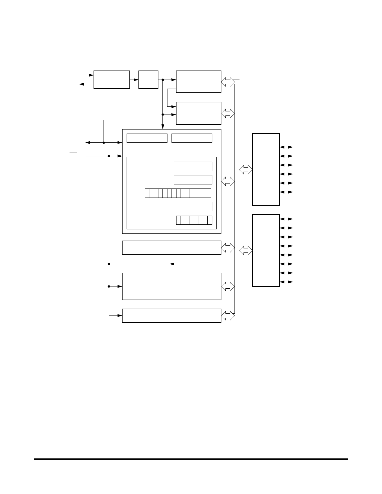
A functional block diagram of the MC68HC705J1A is shown in
Figure 1-1.
Technical Data MC68HC705J1A — Rev. 4.0
22 General Descri ptio n MOTOR OLA
Page 23
General Description
Introduction
OSC1
OSC2
RESET
IRQ/V
PP
INTERNAL
OSCILLATOR
DIVIDE
BY ³2
68HC05 CPU
CPU REGISTERS
0000000011
PROGRAM COUNTER
CONDITION CODE
REGISTER
STATIC RAM (SRAM) — 64 BYTES
USER EPROM — 1240 BYTES
15-STAGE
MULTIFUNCTION
TIMER SYSTEM
WATCHDOG AND
ILLEGAL ADDRESS
ALUCPU CONTROL
ACCUMULATOR
INDEX REGISTER
111HINZC
DETECT
STK PTR
PB5
PB4
PB3
PB2
PB1
PB0
PA7*
PA6*
PA5*
PA4*
PORT A PORT B
DATA DIRECTION REGISTER A DATA DIRECTION REGISTER B
*10-m A si nk capability
**External interrupt capability
PA3* *
PA2* *
PA1* *
PA0* *
MASK OPTION REGISTER (EPROM)
Figure 1-1. Block Diagram
MC68HC705J1A — Rev. 4.0 Technical Data
MOTOROLA General Description 23
Page 24

General Description
1.3 Features
Features of the MC68HC705J1A include:
• Periphera l modules:
– 15-stage multifunction timer
– Computer operating properly (COP) watchdog
• 14 bidirectional input/output (I/O) lines, including:
– 10-mA sink capability on four I/O pins
– Mask option register (MOR) and software programmable
pulldowns on all I/O pins
– MOR selectable interrupt on four I/O pins, a keyboard scan
feature
• MOR selectable sensitivity on external interrupt (edge- and
level-sensitive or edge-sensitive only)
• On-chip oscillator with connections for:
– Crystal
– Ceramic resonator
– Resistor-capacitor (RC) oscillator
– External clock
• 1240 bytes of EPROM/OTPROM, including eight bytes for user
vectors
• 64 bytes of user random-access memory (RAM)
• Memory-mapped I/O registers
• Fully static operation with no minimum clock speed
• Power-saving stop, halt, wait, and data-retention modes
• External interrupt mask bit and acknowledge bit
• Illegal address reset
• Internal steer ing d iode and pullup resistor from RES ET
pin to V
DD
Technical Data MC68HC705J1A — Rev. 4.0
24 General Descri ptio n MOTOR OLA
Page 25

1.4 Programmable Options
The options in Table 1-1 are programm abl e in the mask option register
(MOR).
COP watchdog timer Enabled or disabled
External interrupt triggering Edge-sensitive only or edge- and level-sensitive
General Description
Programmable Options
Table 1-1. Programmable Options
Feature Option
Port A IRQ
Port pulldown resistors Enabled or disabled
STOP instruction mode Stop mode or halt mode
Crystal oscillator internal resistor Enabled or disabled
EPROM security Enabled or disabled
Short oscillator delay counter Enabled or disabled
1.5 Pin Assignments
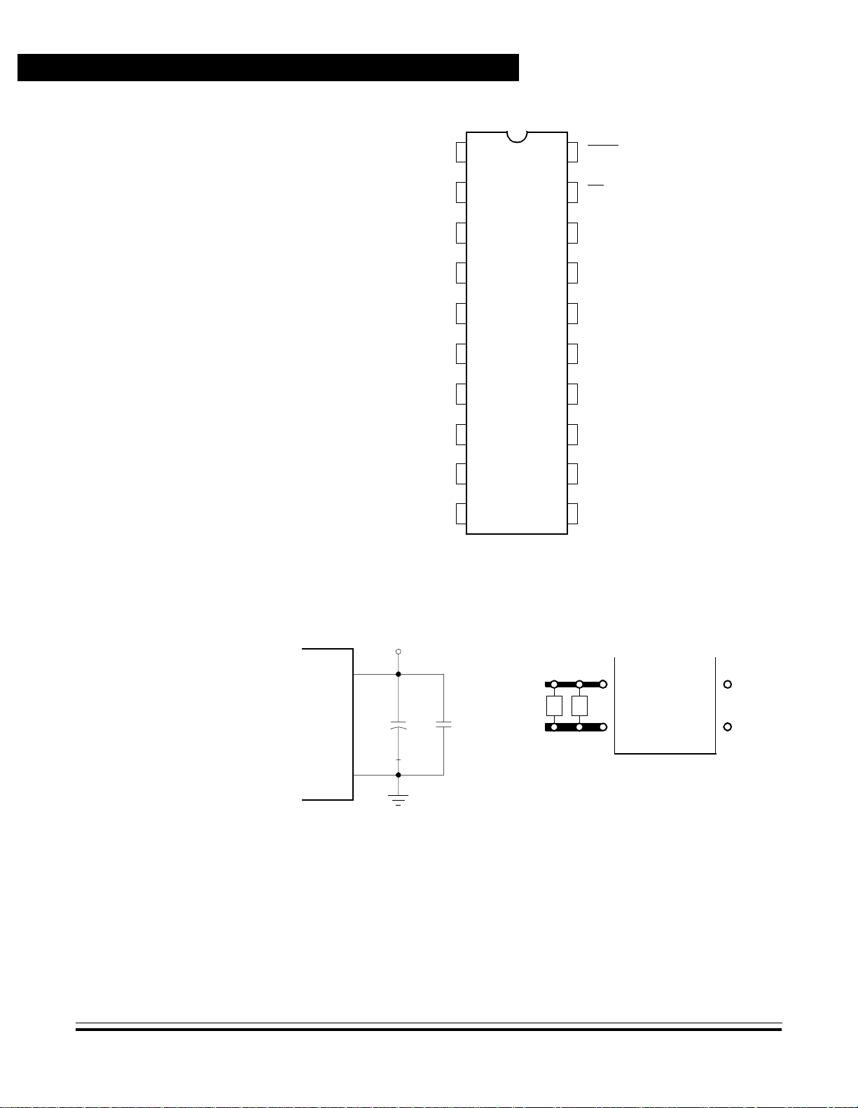
Figure 1-2 shows the MC68HC705J1A pin assignments.
1.5.1 VDD and V
SS
VDD and VSS are the power supply and g round pins. The MCU opera tes
from a single power supply.
Very fast signal transitions occur on the MCU pins, placing high,
short-duration current demands on the power supply. To prevent noise
problems, take special care as Figure 1-3 shows, by placing the bypas s
capacitors as close as possible to the MCU. C2 is an optional bulk
current bypass capaci tor for use in appl ications that requi re the port pi ns
to source high current levels.
pin interrupts Enabled or disabled
MC68HC705J1A — Rev. 4.0 Technical Data
MOTOROLA General Description 25
Page 26
General Description
OSC1
OSC2 2
PB5 3
PB4 4
PB3 5
PB2 6
PB1 7
PB0 8
V
DD
V
SS
1
9
10
RESET
20
IRQ/V
19
12
11
PP
PA018
PA117
PA216
PA315
PA414
PA513
PA6
PA7
Figure 1-2. Pin Assignments
V+
V
MCU
DD
C1
0.1 µF
V
SS
C2
+
C2
C1
V
DD
V
SS
Figure 1-3. Bypassing Layout Recommendation
Technical Data MC68HC705J1A — Rev. 4.0
26 General Descri ptio n MOTOR OLA
Page 27

1.5.2 OSC1 and OSC2
General Description
Pin Assignments
The OSC1 and OSC2 pins are the connections for the on-chip oscillator.
The oscillator can be driven by any of these:
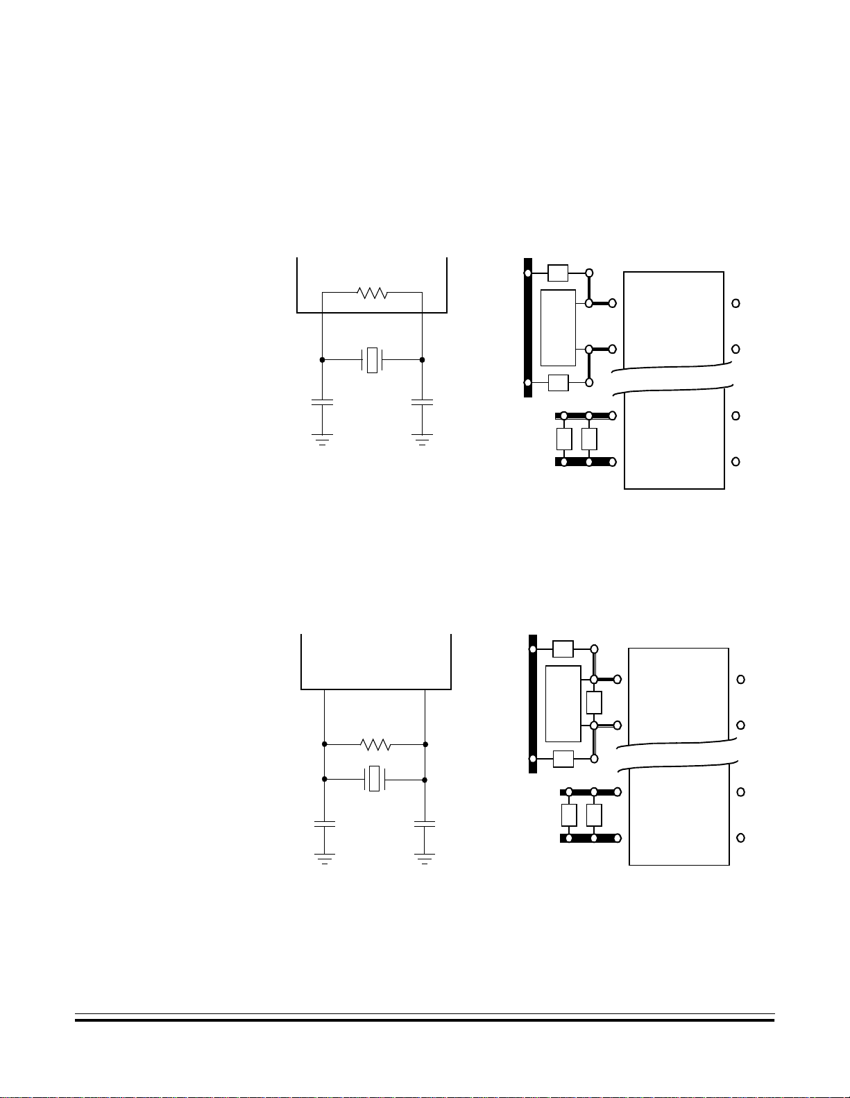
1. Crystal (See Figure 1-4 and Figure 1-5.)
2. Ceramic resonator (See Figure 1-6 and Figure 1-7.)
3. Resistor/capacitor (RC) oscillator (Refer to Appendix A.
MC68HRC705J1A and Appendix C. MC68HSR705J1A.)
4. External clock signal (See Figure 1-8.)
1.5.2.1 Crystal Oscillator
NOTE: Use an AT-cut crystal and not an AT -strip crystal becau se the MCU can
The frequency, f
by two to produce the internal operating frequency, f
, of the oscillator or external clock source is divided
osc
.
op
Figure 1-4 and Figur e 1- 5 show a typica l crystal oscillator circuit for an
AT-cut, parallel re sonant crystal. Follow the crystal supplier’s
recommendations, as the crystal parameters determine the external
component values required to provide reliable startup and maximum
stability. The loa d capacitance values used in the oscilla tor circuit design
should include all stray layout capacitances.
To minimize out put distortion, mount the crystal an d capacitors a s close
as possible to the pins. An internal startup resistor of approximately
2MΩ is provided between OSC1 and OSC2 for the crystal oscillator as
a programmable mask option.
overdrive an AT-strip crystal.
MC68HC705J1A — Rev. 4.0 Technical Data
MOTOROLA General Description 27
Page 28

General Description
V
SS
MCU
OSC1
OSC2
C3
OSC1
XTAL
OSC2
C3
27 pF
C3
27 pF
XTAL
C4
27 pF
C4
C1C2
Figure 1-4. Crystal Connections with
Oscillator Internal Resistor Mask Option
V
SS
MCU
R
OSC1
10 M¾Ω
XTAL
OSC2
27 pF
C4
C3
XTAL
C4
R
C1C2
V
DD
V
SS
OSC1
OSC2
V
DD
V
SS
Figure 1-5. Crystal Connections without
Oscillator Internal Resistor Mask Option
1.5.2.2 Ceramic Resonator Oscillator
To reduce cost, use a ceramic resonator instead of the crystal. The
circuits shown in Figure 1-6 and Figure 1-7 show ceramic resonator
circuits. Follow the resonator manufacturer’s recommendations, as the
resonator parameters determine the external component values
required for maximum stability and reliable starting. The load
capacitance values used in the o scillator circuit d esign should include all
stray capacitances.
Technical Data MC68HC705J1A — Rev. 4.0
28 General Descri ptio n MOTOR OLA
Page 29
General Description
Pin Assignments
Mount the resonator and components as close as possible to the pins for
startup stabilization and to min imize output distortion. An internal startup
resistor of approximat ely 2 MΩ is provided between OSC1 and OSC2 as
a programmable mask option.
V
SS
MCU
C3
OSC1
C3
27 pF
OSC1
CERAMIC
RESON ATOR
OSC2
C4
27 pF
C4
CERAMIC
RESON ATOR
C1C2
OSC2
V
DD
V
SS
Figure 1-6. Ceramic Resonator Connections
with Oscillator Internal Resistor Mask Option
V
SS
C3
OSC1
R
CERAMIC
RESON ATOR
OSC2
OSC1
MCU
R
10 M¾Ω
OSC2
C4
V
DD
V
SS
C3
27 pF
CERAMIC
RESON ATOR
C4
27 pF
C1C2
Figure 1-7. Ceramic Resonator Connections
without Oscillator Internal Resistor Mask Option
MC68HC705J1A — Rev. 4.0 Technical Data
MOTOROLA General Description 29
Page 30

General Description
1.5.2.3 RC Oscillator
1.5.2.4 External Clock
Refer to Appendix A. MC68HRC705J1A and Appendix C.
MC68HSR705J1A.
An external clock from another complementary metal-oxide
semiconductor (CMOS)-compatible device can be connected to the
OSC1 input, with the OSC2 input not connected, as shown in
Figure 1-8. This configuration is possible regardless of whether the
crystal/ceramic resonator or the RC oscillator is enabled.
MCU
1.6 RESET
OSC1
EXTERNAL
CMOS CLOCK
OSC2
Figure 1-8. External Clock Connections
Applying a logic 0 to the RE SET pin for ces the M CU to a known startup
state. An internal r eset also pulls the RESET pin low. An internal resist or
to VDD pulls the RESET pin hi gh. A steeri n g diode b etween the RESET
and V
pins discharges any RESET pin voltage when power is
DD
removed from the MCU. The RESET pin contains an internal Schmitt
trigger to improve its noise immunity as an input. Refer to Section 4.
Resets and Interrupts for more information.
Technical Data MC68HC705J1A — Rev. 4.0
30 General Descri ptio n MOTOR OLA
Page 31

General Description
IRQ/V
PP
1.7 IRQ/V
PP
The external interrupt/programming voltage pin (IRQ/VPP) drives the
asynchronous IRQ interrupt function of the CPU. Additionally, it is used
to progra m t he u ser EPROM and mask option registe r. (Se e S ect ion 2.
Memory and Section 8. External Interrupt Module (IRQ).)
The LEVEL bit in the mask option register provides negative
edge-sensitive triggering or both negative edge-sensitive and low
level-sensitive triggering for the interrupt function.
If level-sensitive triggering is selected, the IRQ/VPP input requires an
external resistor to VDD for wired- OR operat ion. I f the IRQ /VPP pin is not
used, it must be tied to the V
supply.
DD
The IRQ/VPP pin contains an internal Schmitt trigger as part of its input
to improve noise immunity. The voltage on this pin should not exceed
V
except when the pin is being used for programming the EPROM.
DD
NOTE: The mask option register can enable the PA0–PA3 pins to function as
external interrupt pins.
1.8 PA0–PA7
These eight input/ou tput (I/O) li nes comprise por t A, a general- purpose,
bidirectional I/O port. See Sectio n 8. E xte rnal In ter rupt Mod ule (IR Q)
for information on PA0–PA3 external interrupts.
1.9 PB0–PB5
These six I/O lines comprise port B, a general- purpose, bidirectiona l I/O
port.
MC68HC705J1A — Rev. 4.0 Technical Data
MOTOROLA General Description 31
Page 32

General Description
Technical Data MC68HC705J1A — Rev. 4.0
32 General Descri ptio n MOTOR OLA
Page 33

Technical Data — MC68HC705J1A
2.1 Contents
2.2 Introduction. . . . . . . . . . . . . . . . . . . . . . . . . . . . . . . . . . . . . . . .33
2.3 Memory Map. . . . . . . . . . . . . . . . . . . . . . . . . . . . . . . . . . . . . . .34
2.4 Input/Output Register Summary. . . . . . . . . . . . . . . . . . . . . . . .35
2.5 RAM . . . . . . . . . . . . . . . . . . . . . . . . . . . . . . . . . . . . . . . . . . . . .37
2.6 EPROM/OTPROM . . . . . . . . . . . . . . . . . . . . . . . . . . . . . . . . . .38
2.6.1 EPROM/OTPROM Programming. . . . . . . . . . . . . . . . . . . . .38
2.6.2 EPROM Programming Register . . . . . . . . . . . . . . . . . . . . .39
2.6.3 EPROM Erasing. . . . . . . . . . . . . . . . . . . . . . . . . . . . . . . . . .40
Section 2. Memory
2.2 Introduction
2.7 Mask Option Register. . . . . . . . . . . . . . . . . . . . . . . . . . . . . . . .40
2.8 EPROM Programming Characteristics. . . . . . . . . . . . . . . . . . .43
This section describes the organization of the on-chip memory
consisting of:
• 1232 bytes of user erasable, programmable read-only memory
(EPROM), plus eight bytes for user vectors
• 64 bytes of user random-access memory (RAM)
MC68HC705J1A — Rev . 4.0 Technical Data
MOTOR OL A Memory 33
Page 34

Memory
2.3 Memory Map
Port A Data Register (PORTA) $0000
Port B Data Register (PORTB) $0001
Unimplemented
Data Direction Register A (DDRA) $0004
Data Direction Register B (DDRB) $0005
Unimplemented
Timer Status and Control Register (TSCR) $0008
Timer Control Register (TCR) $0009
$0000
↓
$001F ↓
$0020
↓ Pulldown Register Port A (PDRA) $0010
$00BF Pulldown Register Port B (PDRB) $0011
$00C0
↓ ↓
$00FF $0017
$0100
↓
$02FF ↓
$0300
↓ Reserved $001F
$07CF
$07D0
↓ Mask Option Register (MOR) $07F1
$07ED
$07EE
$07EF $07F7
$07F0
↓ Timer Interrupt Vector Low $07F9
$07FF External Interrupt Vector High $07FA
(1)
Writing to bit 0 of $07F0 clears the computer
operating properly (COP) watchdog.
I/O Registers
32 Bytes
Unimplemented
160 Bytes
RAM
64 Bytes
Unimplemented
512 Bytes
EPROM
1232 Bytes
Unimplemented
30 Bytes
Test ROM
2 Bytes
Registers and EPROM
16 Bytes
IRQ Status and Control Register (ISCR) $000A
Unimplemented
Unimplemented
EPROM Programming Register (EPROG) $0018
Unimplemented
COP Register (COPR)
Reserved
Timer Interrupt Vector High $07F8
External Interrupt Vector Low $07FB
Software Interrupt Vector High $07FC
Software Interrupt Vector Low $07FD
Reset Vector High $07FE
Reset Vector Low $07FF
(1)
$0002
$0003
$0006
$0007
$000B
$000F
$0012
$0019
$001E
$07F0
$07F2
↓
Figure 2-1. Memory Map
Technical Data MC68HC705J1A — Rev. 4.0
34 Memory MOTOROLA
Page 35

Memory
Input/Output Register Summary
2.4 Input/Output Regist er Summary
Addr.Register Name Bit 7654321Bit 0
Port A Data Register
$0000
Port B Data Register
$0001
$0002 Unimplemented
$0003 Unimplemented
Data Direction Register A
$0004
Data Direction Register B
$0005
(PORTA)
See page 89.
(PORTB)
See page 92.
(DDRA)
See page 90.
(DDRB)
See page 93.
Read:
PA7 PA6 PA5 PA4 PA3 PA2 PA1 PA0
Write:
Reset: Unaffected by reset
Read: 0 0
PB5 PB4 PB3 PB2 PB1 PB0
Write:
Reset: Unaffected by reset
Read:
DDRA7 DDRA6 DDRA5 DDRA4 DDRA3 DDRA2 DDRA1 DDRA0
Write:
Reset:00000000
Read: 0 0
DDRB5 DDRB4 DDRB3 DDRB2 DDRB1 DDRB0
Write:
Reset:00000000
$0006 Unimplemented
$0007 Unimplemented
$0008
Timer Status and Control
Register (TSCR)
See page 112.
Read: TOF RTIF
TOIE RTIE
Write: TOFR RTIFR
Reset:00000011
= Unimplemented R = Reserved
00
RT1 RT0
Figure 2-2. I/O Register Summary (Sheet 1 of 3)
MC68HC705J1A — Rev. 4.0 Technical Data
MOTOR OL A Memory 35
Page 36

Memory
Addr.Register Name Bit 7654321Bit 0
Timer Counter Register
$0009
See page 114.
IRQ Status and Control
$000A
$000B Unimplemented
↓
$000F Unimplemented
$0010
$0011
Register (ISCR)
See page 106.
Pulldown Register A
Pulldown Register B
(TCR)
(PDRA)
See page 91.
(PDRB)
See page 94.
Read: TMR7 TMR6 TMR5 TMR4 TMR3 TMR2 TMR1 TMR0
Write:
Reset:00000000
Read:
IRQE
Write:
Reset:10000000
Read:
Write: PDIA7 PDIA6 PDIA5 PDIA4 PDIA3 PDIA2 PDIA1 PDIA0
Reset:00000000
Read:
Write: PDIB5 PDIB4 PDIB3 PDIB2 PDIB1 PDIB0
Reset:00000000
000IRQF000
R IRQR
$0012 Unimplemented
↓
$0017 Unimplemented
Read: 0 0 0 0 0
ELAT MPGM EPGM
Write: RRRR
Reset:00000000
= Unimplemented R = Reserved
$0018
EPROM Programming
Register (EPROG)
See page 39.
Figure 2-2. I/O Register Summary (Sheet 2 of 3)
Technical Data MC68HC705J1A — Rev. 4.0
36 Memory MOTOROLA
Page 37

Memory
RAM
Addr.Register Name Bit 7654321Bit 0
$0019 Unimplemented
↓
$001E Unimplemented
$001F Reserved RRRRRRRR
$07F0
Mask Option Register
$07F1
2.5 RAM
COP Register
(COPR)
See page 99.
(MOR)
See page 41.
Figure 2-2. I/O Register Summary (Sheet 3 of 3)
Read:
Write: COPC
Reset: 0
Read:
SOSCD EPMSEC OSCRES SWAIT SWPDI PIRQ LEVEL COPEN
Write:
Reset: Unaffected by reset
= Unimplemented R = Reserved
The 64 addresse s from $00C0 to $00FF serve as both the user RAM and
the stack RAM. Before processing an interrupt, the central processor
unit (CPU) uses five bytes of the stack to save the contents of the CPU
registers. During a sub rout ine call , th e CPU uses two bytes o f the stack
to store the re turn address. The stack po inter decrements when the CPU
stores a byte on the sta ck and increments when the C PU retrieves a byte
from the stack.
NOTE: Be careful when using nested subroutines or multiple interrupt levels.
The CPU may overwrite data in the RAM during a subroutine or during
the interrupt stacking operation.
MC68HC705J1A — Rev. 4.0 Technical Data
MOTOR OL A Memory 37
Page 38

Memory
2.6 EPROM/OTPROM
NOTE: Keep the quartz window covered with an opaque material except when
A microcontroller unit (MCU) with a quartz window has 1240 bytes of
erasable, programmable ROM (EPROM). The quartz window allows
EPROM erasure with ultraviolet light.
programming the MCU. Ambient light can affect MCU operation.
In an MCU without the quartz window, the EPROM cannot be erased
and serves as 1240 bytes of one- time pr ogra mma ble RO M (OT PROM).
These addresses are user EPROM/OTPROM locations:
• $0300–$07CF
• $07F8–$07FF, used for user-defined interrupt and reset vectors
The computer operating properly (COP) register (COPR) is an
EPROM/OTPROM location at address $07F0.
The mask option register (MOR) is an EPROM/OTPROM location at
address $07F1.
2.6.1 EPROM/OTPROM Programming
The two ways to program the EPROM/OTPROM are:
1. Manipulating the control bits in the E PROM pro gramming regi ster
to program the EPROM/OTPROM on a byte-by-byte basis
2. Programming the EPROM/OTPROM with the M68HC705J
in-circuit simulator (M68HC705JICS) available from Motorola
Technical Data MC68HC705J1A — Rev. 4.0
38 Memory MOTOROLA
Page 39

2.6.2 EPROM Programming Register
The EPROM programming register (EPROG) contains the control bits
for programming the EPROM/OTPROM.
Address: $0018
Bit 7654321Bit 0
Read: 0 0 0 0 0
Write:
Reset:00000000
= Unimplemented R = Reserved
Figure 2-3. EPROM Programming Register (EPROG)
ELAT — EPROM Bus Latch Bit
Memory
EPROM/OTPROM
ELAT MPGM EPGM
RRRR
This read/write bit latches the address and data buses for
EPROM/OTPROM p rogramming. Cl earing the ELAT bit automatical ly
clears the EPGM bit. EPROM/OTPROM data cannot be read while
the ELAT bit is set. Reset clears the ELAT bit.
1 = Address and data buses configured for EPROM/OTPROM
programming the EPROM
0 = Address and data buses configured for normal operation
MPGM — MOR Programming Bit
This read/write bit appl ies prog ram ming power from the IRQ/VPP pin
to the mask option register. Reset clears MPGM.
1 = Programming voltage applied to MOR
0 = Programming voltage not applied to MOR
EPGM — EPROM Programming Bit
This read/write bit applies the voltage from the IRQ/V
pin to the
PP
EPROM. To write the EPGM bit, the ELAT bit must be set already.
Reset clears EPGM.
1 = Programming voltage (IRQ/VPP pin) applied to EPROM
0 = Programming voltage (IRQ/VPP pin) not applied to EPROM
MC68HC705J1A — Rev. 4.0 Technical Data
MOTOR OL A Memory 39
Page 40

Memory
NOTE: Writing logic 1s to both the ELAT and EPG M bits with a s ingle instructi on
sets ELAT and clears EPGM. ELAT must be set first by a separate
instruction.
Bits [7:3] — Reserved
Take these steps to program a byte of EPROM/OTPROM:
1. Apply the programming voltage, VPP, to the IRQ/VPP pin.
2. Set the ELAT bit.
3. Write to any EPROM/OTPROM address.
4. Set the EPGM bit and wait for a time, t
5. Clear the ELAT bit.
2.6.3 EPROM Erasing
The erased state of an EPROM bit is logic 0. Erase the EPROM by
exposing it to 15 Ws/cm
2537 angstroms. Position the ultraviolet light source one inch from the
EPROM. Do not use a shortwave filter.
2.7 Ma sk Option Register
The mask option register (MOR) is an EPROM/OTPROM byte that
controls these options:
• COP watchdog (enable or disable)
• External in terr upt pin triggering (edge-sensitiv e o nly or ed ge- and
level-sensitive)
.
EPGM
2
of ultraviolet light with a wave length of
• Port A external interrupts (enable or disable)
• Port pulldown resistors (enable or disable)
• STOP instruction (stop mode or halt mode)
• Crystal oscillator internal resistor (enable or disable)
• EPROM security (enable or disable)
• Short oscillator delay (enable or disable)
Technical Data MC68HC705J1A — Rev. 4.0
40 Memory MOTOROLA
Page 41

Take these steps to program the mask option register:
Memory
Mask Option Register
1. Apply the programming voltage, V
, to the IRQ/VPP pin.
PP
2. Write to the MOR.
3. Set the MPGM bit and wait for a time, t
MPGM
.
4. Clear the MPGM bit.
5. Reset the MCU.
Address: $07F1
Bit 7654321Bit 0
Read:
Write:
Reset: Unaffected by reset
SOSCD EPMSEC OSCRES SWAIT SWPDI PIRQ LEVEL COPEN
Figure 2-4. Mask Option Register (MOR)
SOSCD — Short Oscillator Delay Bit
The SOSCD bit controls the oscillator stabilization counter. The
normal stabilization delay following reset or exit from stop mode is
4064 t
. Setting SOSCD enables a short oscillator stabilization
cyc
delay.
1 = Short oscillator delay enabled
0 = Short oscillator delay disabled
EPMSEC — EPROM Security Bit
The EPMSEC bit controls access to the EPROM/OTPROM.
1 = External access to EPROM/OTPROM denied
0 = External access to EPROM/OTPROM not denied
OSCRES — Oscillator Internal Resistor Bit
The OSCRES bit enables a 2-MΩ internal resistor in the oscillator
circuit.
1 = Oscillator internal resistor enabled
0 = Oscillator internal resistor disabled
NOTE: Program the OSCRES bit to logic 0 in devices using RC oscillators.
MC68HC705J1A — Rev. 4.0 Technical Data
MOTOR OL A Memory 41
Page 42

Memory
SWAIT — Stop-to-Wait Conversion Bit
The SWAIT bit enables halt mode. When the SWAIT bit is set, the
CPU interprets the STOP instruction as a WAIT instruction, and the
MCU enters halt mode. H alt mode is the same as wait mo de, except
that an oscillator stabilization delay of 1 to 4064 t
occurs after
cyc
exiting halt mode.
1 = Halt mode enabled
0 = Halt mode not enabled
SWPDI — Software Pulldown Inhibit Bit
The SWPDI bit inhibits software control of the I/O port pulldown
devices. The SW PDI bi t over rides t he pu lld own inhib it bits in the port
pulldown inhibit registers.
1 = Software pulldown control inhibited
0 = Software pulldown control not inhibited
PIRQ — Port A External Interrupt Bit
The PIRQ bit enables the PA0–PA3
pins to function as external
interrupt pins.
1 = PA0–PA3 enabled as external interrupt pins
0 = PA0–PA3 not enabled as external interrupt pins
LEVEL —External Interrupt Sensitivity Bit
The LEVEL bit controls external interrupt triggering sensitivity.
1 = External interrupts triggered by active edges and active levels
0 = External interrupts triggered only by active edges
COPEN — COP Enable Bit
The COPEN bit enables the COP watchdog.
1 = COP watchdog enabled
0 = COP watchdog disabled
Technical Data MC68HC705J1A — Rev. 4.0
42 Memory MOTOROLA
Page 43

2.8 EPROM Programming Characteristics
Memory
EPROM Programming Characteristics
Characteristic
Programming voltage
/V
IRQ
PP
Programming current
IRQ/V
PP
(1)
Symbol Min Typ Max Unit
V
PP
I
PP
16.0 16.5 17.0 V
—¦ 3.0 10.0 mA
Program ming time
t
Per array byte
MOR
1. VDD = 5.0 Vdc ± 10%, VSS = 0 Vdc, TA = –40°C to +105°C
EPGM
t
MPGM
4
4
—
—
—
—
ms
MC68HC705J1A — Rev. 4.0 Technical Data
MOTOR OL A Memory 43
Page 44

Memory
Technical Data MC68HC705J1A — Rev. 4.0
44 Memory MOTOROLA
Page 45

Technical Data — MC68HC705J1A
Section 3. Central Processor Unit (CPU)
3.1 Contents
3.2 Introduction. . . . . . . . . . . . . . . . . . . . . . . . . . . . . . . . . . . . . . . .46
3.3 CPU Control Unit . . . . . . . . . . . . . . . . . . . . . . . . . . . . . . . . . . .46
3.4 Arithmetic/Logic Unit. . . . . . . . . . . . . . . . . . . . . . . . . . . . . . . . .46
3.5 CPU Registers . . . . . . . . . . . . . . . . . . . . . . . . . . . . . . . . . . . . .48
3.5.1 Accumulator . . . . . . . . . . . . . . . . . . . . . . . . . . . . . . . . . . . . .48
3.5.2 Index Register . . . . . . . . . . . . . . . . . . . . . . . . . . . . . . . . . . .48
3.5.3 Stack Pointer . . . . . . . . . . . . . . . . . . . . . . . . . . . . . . . . . . . .49
3.5.4 Program Counter . . . . . . . . . . . . . . . . . . . . . . . . . . . . . . . . .50
3.5.5 Condition Code Register . . . . . . . . . . . . . . . . . . . . . . . . . . .50
3.6 Instruction Set. . . . . . . . . . . . . . . . . . . . . . . . . . . . . . . . . . . . . .52
3.6.1 Addressing Modes . . . . . . . . . . . . . . . . . . . . . . . . . . . . . . . .52
3.6.1.1 Inherent . . . . . . . . . . . . . . . . . . . . . . . . . . . . . . . . . . . . . .52
3.6.1.2 Immediate . . . . . . . . . . . . . . . . . . . . . . . . . . . . . . . . . . . .52
3.6.1.3 Direct . . . . . . . . . . . . . . . . . . . . . . . . . . . . . . . . . . . . . . . .53
3.6.1.4 Extended . . . . . . . . . . . . . . . . . . . . . . . . . . . . . . . . . . . . .53
3.6.1.5 Indexed, No Offset. . . . . . . . . . . . . . . . . . . . . . . . . . . . . .53
3.6.1.6 Indexed, 8-Bit Offset . . . . . . . . . . . . . . . . . . . . . . . . . . . .53
3.6.1.7 Indexed, 16-Bit Offset . . . . . . . . . . . . . . . . . . . . . . . . . . .54
3.6.1.8 Relative . . . . . . . . . . . . . . . . . . . . . . . . . . . . . . . . . . . . . .54
3.6.2 Instruction Types . . . . . . . . . . . . . . . . . . . . . . . . . . . . . . . . .55
3.6.2.1 Register/Memory Instructions . . . . . . . . . . . . . . . . . . . . .55
3.6.2.2 Read-Modify-Write Instructions . . . . . . . . . . . . . . . . . . . .56
3.6.2.3 Jump/Branch Instructions . . . . . . . . . . . . . . . . . . . . . . . .57
3.6.2.4 Bit Manipulation Instructions . . . . . . . . . . . . . . . . . . . . . .59
3.6.2.5 Control Instructions . . . . . . . . . . . . . . . . . . . . . . . . . . . . .60
3.7 Instruction Set Summary . . . . . . . . . . . . . . . . . . . . . . . . . . . . .61
3.8 Opcode Map. . . . . . . . . . . . . . . . . . . . . . . . . . . . . . . . . . . . . . .66
MC68HC705J1A — Rev . 4.0 Technical Data
MOTOROLA Central Processor Unit (CPU) 45
Page 46

Central Processor Unit (CPU)
3.2 Introduction
The central processor unit (CPU) consists of a CPU control unit, an
arithmetic/l ogic unit (ALU), and five C PU registers. Th e CPU control unit
fetches and decodes instructions. The ALU executes the instructions.
The CPU registers contain data, addresses, and status bits that reflect
the results of CPU operations. See Figure 3-1.
Features include:
• 2.1-MHz bus frequency
• 8-bit accumulator
• 8-bit index register
• 11-bit program counter
• 6-bit stack pointer
• Condition code register (CCR) with five status flags
• 62 instructions
• Eight addressing modes
• Power-saving stop, wait, halt, and data-retention modes
3.3 CPU Control Unit
The CPU control unit fetches and decodes instructions during program
operation. The control unit selects the memory locations to read and
write and coordinates the timing of all CPU operations.
3.4 Arithmetic/Logic Unit
The arithmetic/logic unit (ALU) performs the arithmetic, logic, and
manipulation operations decoded from the instruction set by the CPU
control unit. The A LU produces the resu lts called for by the pro gram and
sets or clears status and control bits in the condition code register
(CCR).
Technical Data MC68HC705J1A — Rev. 4.0
46 Central Processor Unit (CPU) MOTOROLA
Page 47

Central Processor Unit (CPU)
Arithmetic/Logic Unit
CPU CONTROL UNIT
0
000000011
0
00
0
0
HALF-CARRY FLAG
INTERRUPT MASK
ARITHMETIC/LOGIC UNIT
04756 321
04756 321
04756 32181215 1314 11 10 9
04756 32181215 1314 11 10 9
04756 321
111HINZC
ACCUMULATOR (A)
INDEX REGISTER (X)
STACK POINTER (SP)
PROGRAM COUNTER (PC)
CONDITION CODE REGISTER (CCR)
NEGATIVE FLAG
ZERO FLAG
CARRY/BORROW FLAG
Figure 3-1. Programming Model
MC68HC705J1A — Rev. 4.0 Technical Data
MOTOROLA Central Processor Unit (CPU) 47
Page 48

Central Processor Unit (CPU)
3.5 CPU Registers
The M68HC05 CPU contains five registers that control and monitor
microcontroller unit (MCU) operation:
• Accumulator
• Index register
• Stack pointer
• Program counter
• Condition code register
CPU registers are not memory mapped.
3.5.1 Accumulator
3.5.2 Index Register
The accumulator (A) is a general-purpose 8-bit register. The CPU uses
the accumulator to hold operands and results of ALU operations.
Bit 7654321Bit 0
Read:
Write:
Res et: Unaff ected by reset
Figure 3-2. Accumulator (A)
In the indexed addr essing (X) modes, the CPU uses the byte i n the index
register to deter mine th e conditi o nal addr ess of the opera nd. Th e index
register also can serve as a temporary storage location or a counter.
Bit 7654321Bit 0
Read:
Write:
Res et: Unaff ected by reset
Figure 3-3. Index Register (X)
Technical Data MC68HC705J1A — Rev. 4.0
48 Central Processor Unit (CPU) MOTOROLA
Page 49

3.5.3 Stack Pointer
Central Processor Unit (CPU)
CPU Registers
The stack pointer (SP) is a 16-bit register that contains the address of
the next location on the stack. During a reset or after the reset stack
pointer instruction (RSP), the stack pointer is preset to $00FF. The
address in the stack pointer decrements after a byte is stacked and
increments before a byte is unstacked.
Bit
151413121110987654321
Read:0000000011
Write:
Reset:0000000011111111
= Unimplemented
Bit
0
Figure 3-4. Stack Pointe r (SP)
The 10 most significant bits of th e stack po inter are per manently f ixed a t
0000000011, so the stack pointer produces addresses from $00C0 to
$00FF. If subroutines and interrupts use more than 64 stack locations,
the stack pointer wraps around to address $00FF and begins writing
over the previously stored data. A subroutine uses two stack locations;
an interrupt uses five locations.
MC68HC705J1A — Rev. 4.0 Technical Data
MOTOROLA Central Processor Unit (CPU) 49
Page 50

Central Processor Unit (CPU)
3.5.4 Program Counter
The program counter (P C) is a 16-bi t regist er that conta in s the addre ss
of the next instruction or operand to be fetch ed. The five most sig nificant
bits of the program counter are ignored and appear as 00000.
Normally, the address in the pr ogra m counte r auto matical ly incre ments
to the next sequential memory location every time an instruction or
operand is fetched. Jump, branch, and interrupt operations load the
program counter with an address other than that of the next sequential
location.
Bit
151413121110987654321
Read:
Write:
Reset: 0 0 0 0 0 Loaded with vector fr om $07FE and $07FF
3.5.5 Condition Code Register
The condition code r egister (CCR) is a n 8- bit registe r who se t hree mo st
significant bits ar e permanently fixed at 11 1. The condition co de register
contains the interru pt mask and four flags that indica te the results of the
instruction just executed.
Bit 7654321Bit 0
Read: 1 1 1
Write:
Bit
0
Figure 3-5. Program Counter (PC)
HINZC
Reset:111U1UUU
= Unimplemented U = Unaffected
Figure 3-6. Condition Code Register (CCR)
Technical Data MC68HC705J1A — Rev. 4.0
50 Central Processor Unit (CPU) MOTOROLA
Page 51

Central Processor Unit (CPU)
CPU Registers
H — Half-Carry Flag
The CPU sets the half-carry fla g when a carr y occurs betwee n bits 3
and 4 of the accumulator during an ADD (add without carry) or ADC
(add with carry) operation. The half-carry flag is required for
binary-coded decimal (BCD) arithmetic operations.
I — Interrupt Mask Bit
Setting the interrupt mask disables interrupts. If an interrupt request
occurs while the interrupt mask is logic 0, the CPU saves the CPU
registers on the stack, sets the interrupt mask, and then fetches the
interrupt vector. If an interr upt request occurs while the interrupt mask
is logic 1, the interrupt request is latched. Normally, the CPU
processes the latch ed interrupt request as so on as the interrupt mask
is cleared again.
A return-from-interrupt instruction (RTI) unstacks the CPU registers,
restoring the interrupt mask to its cleared state. After any reset, the
interrupt mask is set and can be cleared only by a software
instruction.
N — Negative Flag
The CPU sets the negative flag when an ALU operation produces a
negative result.
Z — Zero Flag
The CPU sets the zero flag when an ALU operati on produces a result
of $00.
C — Carry/Borrow Flag
The CPU sets the carry/borrow flag when an addition operation
produces a carry out of bit 7 of the accumula tor or when a subtraction
operation requires a borrow. Some logical operations and data
manipulation instru ctions also clear or set the carry/borrow flag.
MC68HC705J1A — Rev. 4.0 Technical Data
MOTOROLA Central Processor Unit (CPU) 51
Page 52

Central Processor Unit (CPU)
3.6 Instruction Set
The MCU instruction set has 62 instructions and uses eight addressing
modes.
3.6.1 Addressing Modes
The CPU uses eight addressing modes for flexibility in accessing data.
The addressing modes provide eight different ways for the CPU to find
the data requir ed to execute an instruction. The eight addressing m odes
are:
• Inherent
• Immediate
• Direct
3.6.1.1 Inherent
3.6.1.2 Immediate
• Extended
• Indexed, no offset
• Indexed, 8-bit offset
• Indexed, 16-bit offset
• Relative
Inherent instructions are those that have no operand, such as return
from interr upt ( RTI) a nd sto p (S TOP ). Some of the inherent instructions
act on data in the CPU registers, such as set carry flag (SEC) and
increment accum ulator (INCA). Inherent instructio ns require no operand
address and are one byte long.
Immediate instructions are those that contain a value to be used in an
operation wi th the value in the accumul ator o r index reg ister. Immed iate
instructions require no operand address and are two bytes long. The
opcode is the first byte, and the immediate data valu e is the second byte.
Technical Data MC68HC705J1A — Rev. 4.0
52 Central Processor Unit (CPU) MOTOROLA
Page 53

3.6.1.3 Direct
3.6.1.4 Extended
Central Processor Unit (CPU)
Instructi on Set
Direct instructions can access any of the first 256 me mory locations with
two bytes. The first byte i s the opcod e, and the second is the low byte of
the operand address. In direct addr essing, the CPU autom atical ly uses
$00 as the high byte of the operand address.
Extended instructions use three bytes and can access any address in
memory. The fir st byte i s the opco de; the seco nd and th ird bytes ar e the
high and low bytes of the operand address.
When using the Motor ola assem bler, the programmer does not need to
specify whether an instruction is direct or extended. The assembler
automatically selects the shortest form of the instruction.
3.6.1.5 Indexed, No Offset
Indexed instructions with no offset are 1-byte instructions that can
access data with variable addresses within the first 256 memory
locations. The index register contains the low byte of the effective
address of the operand. The CPU automatically uses $00 as the high
byte, so these instructions can address locations $0000–$00FF.
Indexed, no offset instru ctions are often used to move a pointer thr ough
a table or to hold the address of a frequently used RAM or input/output
(I/O) location.
3.6.1.6 Indexed, 8-Bit Offset
Indexed, 8-b it offset instru cti ons are 2- byte i n structio ns tha t can a ccess
data with varia ble addr esses withi n the first 511 m emor y locati ons. The
CPU adds the unsigned byte in the index register to the unsigned byte
following the opcode. The sum is the effective address of the operand.
These instructions can access locations $0000–$01FE.
Indexed 8-bit offset instructions are usefu l for selecting the kth element
in an n-element table. The table can begin anywhe re within the first 256
memory locations and could extend as far as location 510 ($01FE).
MC68HC705J1A — Rev. 4.0 Technical Data
MOTOROLA Central Processor Unit (CPU) 53
Page 54

Central Processor Unit (CPU)
The k value is typically in the index register, and the address of the
beginning of the table is in the byte following the op code.
3.6.1.7 Indexed, 16-Bit Offset
Indexed, 16-b it offset instructions are 3-byte in structions that can access
data with variabl e ad dresse s at any lo cation i n memo ry. T he C PU adds
the unsigned byte in the index register to the two unsigned bytes
following the opcode. The sum is the effective address of the operand.
The first byte after the opcode is the high byte of the 16-bit offset; the
second byte is the low byte of the offset.
Indexed, 16-b it offset instructions are use ful for selecting the kth element
in an n-element table anywhere in memory.
As with direct and extended addressing, the Motorola assembler
determines the shortest form of indexed addressing.
3.6.1.8 Relative
Relative addressing is only for branch instructions. If the branch
condition is true, the CPU finds the effective branch destination by
adding the signed byte following the opcode to the contents of the
program counter. If the br anch condition is not true, the CPU goes to the
next instruction. The offset is a signed, two’s complem ent byte that gives
a branching range of –128 to +127 bytes from the address of the next
location after the branch instruction.
When using the Motor ola assem bler, the programmer does not need to
calculate the offset because the assembler determ ines the proper offset
and verifies that it is within the span of the branch.
Technical Data MC68HC705J1A — Rev. 4.0
54 Central Processor Unit (CPU) MOTOROLA
Page 55

3.6.2 Instruction Types
The MCU instructions fall into these five categories:
• Register/memory instructions
• Read-modify-write instructions
• Jump/branch instructions
• Bit manipulation instructions
• Control instructions
3.6.2.1 Register/Memory Instructions
These instructions operate on CPU registers and memory locations.
Most of them use two operands. One operand is in either the
accumulator or the index register. The CPU finds the other operand in
memory.
Central Processor Unit (CPU)
Instructi on Set
Table 3-1. Register/Memory Instructions
Instruction Mnemonic
Add memory byte and carry bit to accumulator ADC
Add memory byte to accumulator ADD
AND memory byte with accumulator AND
Bit test accumulator BIT
Compare accumulator CMP
Compare index register with memory byte CP X
EXCLUSIVE OR accu mu lator with memory byte EOR
Load accumulator with memory byte LDA
Load index register with memory byte LDX
Multiply MUL
OR accumulator with memory byte ORA
Subtract memory byte and carry bit from accumulator SBC
Store accu mu lator in memory STA
Store index register in memory STX
Subtract memory byte from accumulator SUB
MC68HC705J1A — Rev. 4.0 Technical Data
MOTOROLA Central Processor Unit (CPU) 55
Page 56

Central Processor Unit (CPU)
3.6.2.2 Read-Modify-Write Instructions
These instructions read a memory location or a register, modify its
contents, and write the modifi ed value b ack to the memory location o r to
the register.
NOTE: Do not use read-modify-write instructions on registers with write-only
bits.
Table 3-2. Read-Modify-Writ e Instruc tion s
Instruction Mnemonic
Arithmetic shift left (same as LSL) ASL
Arithmetic shift right ASR
Bit clear
Bit set
Clear register CLR
Complement (one’s complement) COM
Decrement DEC
Increment INC
Logical shift left (same as ASL) LSL
Logical shift right LSR
Negate (two’s compl eme nt ) NEG
Rotate left through carry bit RO L
Rotate right through carry bit ROR
Test for negative or zero
1. Unlike other read-modify-write instructions, BCLR and
BSET use only direct addressing.
2. TST is an exception to the read -modify-write seq uence
because it does not write a replacement value.
BCLR
BSET
TST
(1)
(1)
(2)
Technical Data MC68HC705J1A — Rev. 4.0
56 Central Processor Unit (CPU) MOTOROLA
Page 57

3.6.2.3 Jump/Branch Instructions
Jump instructions all ow the CPU to interrupt the norma l sequence of the
program counter. The unconditional jump instruction (JMP) and the
jump-to-subroutine instruction (JSR) have no register operand. Branch
instructions allow the CPU to interrupt the normal sequence of the
program counter when a test condition is met. If the test conditi o n is n ot
met, the branch is not performed.
The BRCLR and BRSET i nstructions cause a br anch based on the state
of any readable bit in the first 256 memory locations. These 3-byte
instructions use a combination of direct addressing and relative
addressing. The direct address of the byte to be tested is in the byte
following the opcode. The third byte is the signed offset byte. The CPU
finds the effective branch destination by adding the third byte to the
program counter i f the specified bit tests true . The bit to be teste d and its
condition (set or clear) is part of the opcode. The span of branching is
from –128 to +127 from the addr ess of the next locati on af ter the branch
instruction. The CPU also tr ansfe rs the tested b i t to the carr y/borr ow bit
of the condition code register.
Central Processor Unit (CPU)
Instructi on Set
NOTE: Do not use BRCLR or BRSET instructions on registers with write-only
bits.
MC68HC705J1A — Rev. 4.0 Technical Data
MOTOROLA Central Processor Unit (CPU) 57
Page 58

Central Processor Unit (CPU)
Table 3-3. Jump and Branch Instructions
Instruction Mnemonic
Branch if carry bit clear BCC
Branch if carry bit set BCS
Branch if equal BEQ
Branch if half-carry bit clear BHCC
Branch if half-carry bit set BHCS
Branch if higher BHI
Branch if higher or same BHS
Branch if IRQ
Branch if IRQ
Branch if lower BLO
Branch if lower or same BLS
Branch if interrupt mask clear BMC
Branch if minus BMI
Branch if interrupt mask set BMS
Branch if not equal BNE
Branch if plus BPL
Branch always BRA
Branch if bit clear BRCLR
Branch never BRN
Branch if bit set BRSET
Branch to subroutine BSR
Unconditional jump JMP
pin high BIH
pin low BIL
Jump to subroutine JSR
Technical Data MC68HC705J1A — Rev. 4.0
58 Central Processor Unit (CPU) MOTOROLA
Page 59

3.6.2.4 Bit Manipulation Instructions
The CPU can set or clear any writable bit in the first 256 bytes of
memory, which includes I/O registers and on-chip RAM locations. The
CPU can also test and br anch based on th e state of any bit in an y of the
first 256 memory locations.
Central Processor Unit (CPU)
Instructi on Set
Table 3-4. Bit Manipulation Instructions
Instruction Mnemonic
Bit clear BCLR
Branch if bit clear BRCLR
Branch if bit set BRSET
Bit set BSET
NOTE: Do not use bit manipulatio n instru ctions on r egister s wit h write- only bi ts.
MC68HC705J1A — Rev. 4.0 Technical Data
MOTOROLA Central Processor Unit (CPU) 59
Page 60

Central Processor Unit (CPU)
3.6.2.5 Control Instructions
These instructions act on CPU registers and control CPU operation
during program execution.
Table 3-5. Control Instructions
Instruction Mnemonic
Clear carry bit CLC
Clear interrupt mask CLI
No operation NOP
Reset stack pointer RSP
Return from interrup t RTI
Return from subroutine RT S
Set carry bit SEC
Set interrupt mask SEI
Stop oscillator and enable IR Q
Software interrupt S W I
Transfer accumulator to index register TAX
Transfer index register to accumulator TXA
Stop CPU clock and enable interrupts
pin STOP
WAIT
Technical Data MC68HC705J1A — Rev. 4.0
60 Central Processor Unit (CPU) MOTOROLA
Page 61

3.7 Instruct ion Set Summary
Table 3-6. Instruction Set Summary (Sheet 1 of 6)
Central Processor Unit (CPU)
Instruction Set Summary
Source
Form
ADC #opr
ADC opr
ADC opr
ADC opr,X
ADC opr,X
ADC ,X
ADD #opr
ADD opr
ADD opr
ADD opr,X
ADD opr,X
ADD ,X
AND #opr
AND opr
opr
AND
AND opr,X
AND opr,X
AND ,X
ASL opr
ASLA
ASLX
ASL opr,X
ASL ,X
Effect
Operation Description
on CCR
HINZC
Add with Carry A ← (A) + (M) + (C)
Add with ou t C arr y A ← (A) + (M)
Logica l AND A ← (A) ∧ (M) ——
Arithmetic Shift Left (Same as LSL) ——
C
b7
b0
—
—
0
—
Address
IMM
DIR
EXT
IX2
IX1
IX
IMM
DIR
EXT
IX2
IX1
IX
IMM
DIR
EXT
IX2
IX1
IX
DIR
INH
INH
IX1
IX
Mode
A9
B9
C9
D9
E9
F9
AB
BB
CB
DB
EB
FB
A4
B4
C4
D4
E4
F4
38
48
58
68
78
ii
dd
hh ll
ee ff
ff
ii
dd
hh ll
ee ff
ff
ii
dd
hh ll
ee ff
ff
dd
ff
Cycles
Operand
2
3
4
5
4
3
2
3
4
5
4
3
2
3
4
5
4
3
5
3
3
6
5
Opcode
37
47
57
67
77
11
13
15
17
19
1B
1D
1F
dd
ff
dd
dd
dd
dd
dd
dd
dd
dd
ASR opr
ASRA
ASRX
ASR opr,X
ASR ,X
BCC rel Branch if Carry Bit Clear PC ← (PC) + 2 + rel ? C = 0 ————— REL 24 rr 3
BCLR n opr Clear Bit n Mn ← 0 —————
BCS rel Branch if Carry Bit Set (Same as BLO) PC ← (PC) + 2 + rel ? C = 1 ————— REL 25 rr 3
BEQ rel Branch if Equal PC ← (PC) + 2 + rel ? Z = 1 ————— REL 27 rr 3
BHCC rel Branch if Half-Carry Bit Clear PC ← (PC) + 2 + rel ? H = 0 ————— REL 28 rr 3
BHCS rel Branch if Half-Carry Bit Set PC ← (PC) + 2 + rel ? H = 1 ————— REL 29 rr 3
Arithmetic Shift R ight ——
b7
b0
C
DIR
INH
INH
IX1
IX
DIR (b0)
DIR (b1)
DIR (b2)
DIR (b3)
DIR (b4)
DIR (b5)
DIR (b6)
DIR (b7)
MC68HC705J1A — Rev . 4.0 Technical Data
MOTOROLA Central Processor Unit (CPU) 61
5
3
3
6
5
5
5
5
5
5
5
5
5
Page 62

Central Processor Unit (CPU)
Table 3-6. Instruction Set Summary (Sheet 2 of 6)
Source
Form
BHI rel Branch if Higher PC ← (PC) + 2 + rel ? C ∨ Z = 0 ————— REL 22 rr 3
BHS rel Branch if Higher or Same PC ← (PC) + 2 + rel ? C = 0 ————— REL 24 rr 3
BIH rel Branch if IRQ Pin High PC ← (PC) + 2 + rel ? IRQ = 1 ————— REL 2F rr 3
BIL rel Branch if IRQ Pin Low PC ← (PC) + 2 + rel ? IRQ = 0 ————— REL 2E rr 3
BIT #opr
BIT opr
BIT opr
BIT opr,X
BIT opr,X
BIT ,X
BLO rel Branch if Lower (Same as BCS) PC ← (PC) + 2 + rel ? C = 1 ————— REL 25 rr 3
BLS rel Branch if Lower or Same PC ← (PC) + 2 + rel ? C ∨ Z = 1 ————— REL 23 rr 3
BMC rel Branch if Interrupt Mask Clear PC ← (PC) + 2 + rel ? I = 0 ————— REL 2C rr 3
BMI rel Branch if Minus PC ← (PC) + 2 + rel ? N = 1 ————— REL 2B rr 3
BMS rel Branch if Interrupt Mask Set PC ← (PC) + 2 + rel ? I = 1 ————— REL 2D rr 3
BNE rel Branch if Not Equal PC ← (PC) + 2 + rel ? Z = 0 ————— REL 26 rr 3
BPL rel Branch if Plus PC ← (PC) + 2 + rel ? N = 0 ————— REL 2A rr 3
BRA rel Branch Always PC ← (PC) + 2 + rel ? 1 = 1 ————— REL 20 rr 3
BRCLR n opr rel Branch if Bit n Clear PC ← (PC) + 2 + rel ? Mn = 0 ————
BRN rel Branch Never PC ← (PC) + 2 + rel ? 1 = 0 ————— REL 21 rr 3
BRSET n opr rel Branch if Bit n Set PC ← (PC) + 2 + rel ? Mn = 1 ————
BSET n opr Set Bit n Mn ← 1 —————
Bit Test Accumulator with Memory Byte (A) ∧ (M) ——
Operation Description
on CCR
HINZC
—
Address
IMM
DIR
EXT
IX2
IX1
IX
DIR (b0)
DIR (b1)
DIR (b2)
DIR (b3)
DIR (b4)
DIR (b5)
DIR (b6)
DIR (b7)
DIR (b0)
DIR (b1)
DIR (b2)
DIR (b3)
DIR (b4)
DIR (b5)
DIR (b6)
DIR (b7)
DIR (b0)
DIR (b1)
DIR (b2)
DIR (b3)
DIR (b4)
DIR (b5)
DIR (b6)
DIR (b7)
Mode
A5
B5
C5
D5
E5
F5
01
03
05
07
09
0B
0D
0F
00
02
04
06
08
0A
0C
0E
10
12
14
16
18
1A
1C
1E
Opcode
Operand
ii
dd
hh ll
ee ff
ff
dd rr
dd rr
dd rr
dd rr
dd rr
dd rr
dd rr
dd rr
dd rr
dd rr
dd rr
dd rr
dd rr
dd rr
dd rr
dd rr
dd
dd
dd
dd
dd
dd
dd
dd
Effect
Cycles
2
3
4
5
4
3
5
5
5
5
5
5
5
5
5
5
5
5
5
5
5
5
5
5
5
5
5
5
5
5
Technical Data MC68HC705J1A — Rev. 4.0
62 Central Processor Unit (CPU) MOTOROLA
Page 63

Central Processor Unit (CPU)
Table 3-6. Instruction Set Summary (Sheet 3 of 6)
Instruction Set Summary
Source
Form
BSR rel Branch to Subroutine
CLC Clear Carry Bit C ← 0 ———— 0INH98 2
CLI Clear Interrupt Mask I ← 0 — 0 ——— INH 9A 2
CLR opr
CLRA
CLRX
CLR opr,X
CLR ,X
CMP #opr
CMP opr
CMP opr
CMP opr,X
CMP opr,X
CMP ,X
COM opr
COMA
COMX
COM opr,X
COM ,X
CPX #opr
CPX opr
CPX opr
CPX opr,X
CPX opr,X
CPX ,X
DEC opr
DECA
DECX
DEC opr ,X
DEC ,X
Clear Byte
Compare Accumulator with Memory Byte (A) – (M) ——
Complement Byte ( O ne’s Complement)
Compare Index Register with Memory Byte (X) – (M) ——
Decrement Byte
Operation Description
PC ← (PC) + 2; push (PCL)
SP ← (SP) – 1; push (PCH)
SP ← (SP) – 1
PC ← (PC) + rel
M ← $00
A ← $00
X ← $00
M ← $00
M ← $00
M) = $FF – (M)
M ← (
A ← (
A) = $FF – (A)
X ← (
X) = $FF – (X)
M ← (
M) = $FF – (M)
M ← (
M) = $FF – (M)
M ← (M) – 1
A ← (A) – 1
X ← (X) – 1
M ← (M) – 1
M ← (M) – 1
on CCR
HINZC
————— REL AD rr 6
—— 01—
——
1
—
——
Address
DIR
INH
INH
IX1
IX
IMM
DIR
EXT
IX2
IX1
IX
DIR
INH
INH
IX1
IX
IMM
DIR
EXT
IX2
IX1
IX
DIR
INH
INH
IX1
IX
Mode
3F
4F
5F
6F
7F
A1
B1
C1
D1
E1
F1
33
43
53
63
73
A3
B3
C3
D3
E3
F3
3A
4A
5A
6A
7A
Opcode
Operand
dd
ff
ii
dd
hh ll
ee ff
ff
dd
ff
ii
dd
hh ll
ee ff
ff
dd
ff
Cycles
5
3
3
6
5
2
3
4
5
4
3
5
3
3
6
5
2
3
4
5
4
3
5
3
3
6
5
Effect
EOR #opr
EOR opr
EOR opr
EOR opr,X
EOR opr,X
EOR ,X
INC opr
INCA
INCX
INC opr,X
INC ,X
EXCLUSIVE OR Accumulator with Memory Byte A ← (A) ⊕ (M) ——
M ← (M) + 1
A ← (A) + 1
Increment Byt e
X ← (X) + 1
M ← (M) + 1
M ← (M) + 1
——
IMM
DIR
EXT
—
IX2
IX1
IX
DIR
INH
—
INH
IX1
IX
A8
B8
C8
D8
E8
F8
3C
4C
5C
6C
7C
ii
dd
hh ll
ee ff
ff
dd
ff
MC68HC705J1A — Rev . 4.0 Technical Data
MOTOROLA Central Processor Unit (CPU) 63
2
3
4
5
4
3
5
3
3
6
5
Page 64

Central Processor Unit (CPU)
Table 3-6. Instruction Set Summary (Sheet 4 of 6)
Source
Form
JMP op r
JMP op r
JMP op r,X
JMP op r,X
JMP ,X
JSR opr
JSR opr
JSR opr,X
JSR opr,X
JSR ,X
LDA #opr
LDA op r
LDA op r
LDA op r,X
LDA op r,X
LDA ,X
LDX #opr
LDX op r
LDX op r
LDX op r,X
LDX op r,X
LDX ,X
Effect
Operation Description
on CCR
HINZC
Unconditional Jump PC ← Jump Address —————
PC ← (PC) + n (n = 1, 2, or 3)
Jump to Subroutine
Load Accumulator with Memory Byte A ← (M) ——
Load Index Regist er with Memo ry Byte X ← (M) ——
Push (PCL); SP ← (SP) – 1
Push (PCH); SP ← (SP) – 1
PC ← Effective Address
—————
—
—
Address
DIR
EXT
IX2
IX1
IX
DIR
EXT
IX2
IX1
IX
IMM
DIR
EXT
IX2
IX1
IX
IMM
DIR
EXT
IX2
IX1
IX
Mode
BC
CC
DC
EC
FC
BD
CD
DD
ED
FD
A6
B6
C6
D6
E6
F6
AE
BE
CE
DE
EE
FE
Opcode
dd
hh ll
ee ff
ff
dd
hh ll
ee ff
ff
ii
dd
hh ll
ee ff
ff
ii
dd
hh ll
ee ff
ff
Operand
Cycles
2
3
4
3
2
5
6
7
6
5
2
3
4
5
4
3
2
3
4
5
4
3
38
48
58
68
78
34
44
54
64
74
30
40
50
60
70
AA
BA
CA
DA
EA
FA
dd
ff
dd
ff
dd
ff
ii
dd
hh ll
ee ff
ff
5
3
3
6
5
5
3
3
6
5
5
3
3
6
5
2
3
4
5
4
3
LSL opr
LSLA
LSLX
LSL opr,X
LSL ,X
LSR op r
LSRA
LSRX
LSR op r,X
LSR ,X
MUL Unsigned Multiply X : A ← (X) × (A) 0 ———0INH42 11
NEG opr
NEGA
NEGX
NEG opr,X
NEG ,X
NOP No Operation ————— INH 9D 2
ORA #opr
ORA opr
ORA opr
ORA opr ,X
ORA opr ,X
ORA ,X
Logica l Shift Left (Same as ASL) ——
Logica l Shift Right —— 0
Negate Byte (Two’s Complement)
Logical OR Accumul ator wit h Memory A ← (A) ∨ (M) ——
C
b7
b7
M ← –(M) = $00 – (M)
A ← –(A) = $00 – (A)
X ← –(X) = $00 – (X)
M ← –(M) = $00 – (M)
M ← –(M) = $00 – (M)
0
b0
C0
b0
——
DIR
INH
INH
IX1
IX
DIR
INH
INH
IX1
IX
DIR
INH
INH
IX1
IX
IMM
DIR
EXT
—
IX2
IX1
IX
Technical Data MC68HC705J1A — Rev. 4.0
64 Central Processor Unit (CPU) MOTOROLA
Page 65

Central Processor Unit (CPU)
Table 3-6. Instruction Set Summary (Sheet 5 of 6)
Instruction Set Summary
Source
Form
ROL opr
ROLA
ROLX
ROL opr,X
ROL ,X
ROR opr
RORA
RORX
ROR opr,X
ROR ,X
RSP Reset Stack Pointer SP ← $00FF ————— INH 9C 2
RTI Return from Interrupt
RTS Return from Subroutine
SBC #opr
SBC opr
SBC opr
SBC opr,X
SBC opr,X
SBC ,X
Rotate Byte Left thro ug h Carry Bit ——
Rotate Byte Righ t throug h Carr y Bit ——
Subtract Memory Byte and Carry Bit from
Accumulator
Operation Description
C
b7
b7
SP ← (SP) + 1; Pull (CCR)
SP ← (SP) + 1; Pull (A)
SP ← (SP) + 1; Pull (X)
SP ← (SP) + 1; Pull (PCH)
SP ← (SP) + 1; Pull (PCL)
SP ← (SP) + 1; Pull (PCH)
SP ← (SP) + 1; Pull (PCL)
A ← (A) – (M) – (C) ——
b0
b0
C
on CCR
HINZC
————— INH 81 6
Mode
39
49
59
69
79
36
46
56
66
76
A2
B2
C2
D2
E2
F2
Opcode
Operand
dd
ff
dd
ff
ii
dd
hh ll
ee ff
ff
Address
DIR
INH
INH
IX1
IX
DIR
INH
INH
IX1
IX
INH 80 9
IMM
DIR
EXT
IX2
IX1
IX
Effect
Cycles
5
3
3
6
5
5
3
3
6
5
2
3
4
5
4
3
SEC Set Carry Bit C ← 1 ————1INH99 2
SEI Set Interrupt Mask I ← 1 — 1 ——— INH 9B 2
B7
C7
D7
E7
F7
BF
CF
DF
EF
FF
A0
B0
C0
D0
E0
F0
dd
hh ll
ee ff
ff
dd
hh ll
ee ff
ff
ii
dd
hh ll
ee ff
ff
4
5
6
5
4
4
5
6
5
4
2
3
4
5
4
3
STA opr
STA opr
STA opr,X
STA opr,X
STA ,X
STOP Stop Oscillator and Enable IRQ Pin — 0 ——— INH 8E 2
STX opr
STX opr
STX opr,X
STX opr,X
STX ,X
SUB #opr
SUB opr
SUB opr
SUB opr,X
SUB opr,X
SUB ,X
Store Accumulato r in Memory M ← (A) ——
Store Index Register In Memory M ← (X) ——
Subtract Memory Byte from Accumulator A ← (A) – (M) ——
DIR
EXT
—
IX2
IX1
IX
DIR
EXT
—
IX2
IX1
IX
IMM
DIR
EXT
IX2
IX1
IX
MC68HC705J1A — Rev . 4.0 Technical Data
MOTOROLA Central Processor Unit (CPU) 65
Page 66

Central Processor Unit (CPU)
Table 3-6. Instruction Set Summary (Sheet 6 of 6)
Source
Form
SWI Software Interrupt
TAX Transfer Accumu la tor to Ind e x Reg ister X ← (A) ————— INH 97 2
TST opr
TSTA
TSTX
TST opr,X
TST ,X
TXA Transfer Index Register to Accumulator A ← (X) ————— INH 9F 2
WAIT Stop CPU Clock and Enable Interrupts —
A Accumulator opr O pe r an d ( on e or t wo by t e s)
C Carry/borrow flag PC Program counter
CCR Condition code register PCH Program coun ter high byte
dd Direct address of operand PCL Program counter low byte
dd rr Direct address of operand and relati ve offset of branch instruction REL Relative addressi ng mode
DIR Direct addressing mode rel Relative pr ogram counter offset byte
ee ff High and low bytes of offset in indexed, 16-bit offset addressing rr Relative program counter offset byte
EXT Extended addressing mode SP Stack pointe r
ff Offset byte in indexed, 8-bit off s et addressing X Index register
H H alf-carry flag Z Zero flag
hh ll High and low bytes of operand address in extended addressing # Immediate value
I Interrupt mask ∧ Lo gi cal AND
ii Immediate operand byte ∨ Logi ca l O R
IMM Immediate addressing mode ⊕ Logi cal EXCL US IVE OR
INH Inherent addressi ng mode ( ) Contents of
IX Indexed, no offset addressing mode –( ) Negat ion (two’s complement)
IX1 Index ed, 8-bit offset addressing mode ← Loaded with
IX2 Indexed, 16-bit off set addressing mo de ? If
M Memory location : Concatenated with
N Negative flag
n Any bit — Not affected
Test Memory Byte for Negative or Zero (M) – $00 ——
Operation Description
PC ← (PC) + 1; Push (PCL)
SP ← (SP) – 1; Push (PCH)
SP ← (SP) – 1; Push (X)
SP ← (SP) – 1; Push (A)
SP ← (SP) – 1; Push (CCR)
SP ← (SP) – 1; I ← 1
PCH ← Interrupt Vector High Byte
PCL ← Interrupt Vector Low Byte
Set or cl eared
on CCR
HINZC
— 1 ——— INH 83 10
—
——— INH 8F 2
Address
DIR
INH
INH
IX1
IX
Mode
3D
4D
5D
6D
7D
Opcode
Operand
dd
ff
Effect
Cycles
4
3
3
5
4
3.8 Opcode Map
See Table 3-7.
Technical Data MC68HC705J1A — Rev. 4.0
66 Central Processor Unit (CPU) MOTOROLA
Page 67

MC68HC705J1A — Rev . 4.0 Technical Data
MOTOROLA Central Processor Unit (CPU) 67
Table 3-7. Opcode Map
Bit Manipulation Branch Read-Modify-Write Control Register/Memory
DIR DIR REL DIR INH INH IX1 IX INH INH IMM DIR EXT IX2 IX1 IX
MSB
LSB
0
1
2
3
4
5
6
7
8
9
A
B
C
D
E
F
0123456789ABCDEF
5
BRSET0
3DIR
BRCLR0
3DIR
BRSET1
3DIR
BRCLR1
3DIR
BRSET2
3DIR
BRCLR2
3DIR
BRSET3
3DIR
BRCLR3
3DIR
BRSET4
3DIR
BRCLR4
3DIR
BRSET5
3DIR
BRCLR5
3DIR
BRSET6
3DIR
BRCLR6
3DIR
BRSET7
3DIR
BRCLR7
3DIR
BSET0
2DIR
5
BCLR0
2DIR
5
BSET1
2DIR
5
BCLR1
2DIR
5
BSET2
2DIR
5
BCLR2
2DIR
5
BSET3
2DIR
5
BCLR3
2DIR
5
BSET4
2DIR
5
BCLR4
2DIR
5
BSET5
2DIR
5
BCLR5
2DIR
5
BSET6
2DIR
5
BCLR6
2DIR
5
BSET7
2DIR
5
BCLR7
2DIR
5
2REL
5
2REL
5
2REL
5
2REL
5
2REL
5
2REL
5
2REL
5
2REL
5
2REL
5
2REL
5
2REL
5
2REL
5
2REL
5
2REL
5
2REL
5
2REL
BRA
BRN
BHI
BLS
BCC
BCS/BLO
BNE
BEQ
BHCC
BHCS
BPL
BMI
BMC
BMS
BIL
BIH
3
3
3
3
3
3
3
3
3
3
3
3
3
3
3
3
INH = Inherent REL = Relative
IMM = Immediate IX = Inde xed, No Offset
DIR = Direct IX1 = Indexed, 8-Bit Offset
EXT = Extended IX2 = Indexed, 16-Bit Offset
5
NEG
2DIR
COM
2DIR
LSR
2DIR
ROR
2DIR
ASR
2DIR
ASL/LSL
2DIR
ROL
2DIR
DEC
2DIR
INC
2DIR
TST
2DIR
CLR
2DIR
NEGA
1INH
1INH
5
COMA
1INH
5
LSRA
1INH
5
RORA
1INH
5
ASRA
1INH
5
ASLA/LSLA
1INH
5
ROLA
1INH
5
DECA
1INH
5
1INH
4
TSTA
1INH
5
CLRA
1INH
MUL
INCA
3
NEGX
1INH
11
3
COMX
1INH
3
LSRX
1INH
3
RORX
1INH
3
ASRX
1INH
3
ASLX/LSLX
1INH
3
ROLX
1INH
3
DECX
1INH
3
INCX
1INH
3
TSTX
1INH
3
CLRX
1INH
NEG
COM
LSR
ROR
ASR
ASL/LSL
ROL
DEC
INC
TST
CLR
6
6
6
6
6
6
6
6
6
5
6
3
2IX1
3
2IX1
3
2IX1
3
2IX1
3
2IX1
3
2IX1
3
2IX1
3
2IX1
3
2IX1
3
2IX1
3
2IX1
1IX
1IX
1IX
1IX
1IX
1IX
1IX
1IX
1IX
1IX
1IX
NEG
COM
LSR
ROR
ASR
ASL/LSL
ROL
DEC
INC
TST
CLR
5
1INH
1INH
5
1INH
5
5
5
5
5
5
5
4
1INH
5
1INH
LSB of Opcode in Hexadecimal
RTI
RTS
SWI
STOP
WAIT
9
6
10
TAX
1INH
CLC
1INH
SEC
1INH
CLI
1INH
SEI
1INH
RSP
1INH
NOP
1INH
2
2
TXA
1INH
2
SUB
2IMM
2IMM
2IMM
2IMM
2IMM
2IMM
2IMM
2
2
2IMM
2
2IMM
2
2IMM
2
2IMM
2
2
2REL
2IMM
2
LSB
CMP
SBC
CPX
AND
BIT
LDA
EOR
ADC
ORA
ADD
BSR
LDX
MSB
2
2
2
2
2
2
2
2
2
2
6
2
0
3
SUB
CMP
SBC
CPX
AND
BIT
LDA
STA
EOR
ADC
ORA
ADD
JMP
JSR
LDX
STX
3EXT
3
3EXT
3
3EXT
3
3EXT
3
3EXT
3
3EXT
3
3EXT
4
3EXT
3
3EXT
3
3EXT
3
3EXT
3
3EXT
2
3EXT
5
3EXT
3
3EXT
4
3EXT
2DIR
2DIR
2DIR
2DIR
2DIR
2DIR
2DIR
2DIR
2DIR
2DIR
2DIR
2DIR
2DIR
2DIR
2DIR
2DIR
0
Number of Cycles
5
BRSET0
3DIR
Opcode Mnemonic
Number of Bytes/Addressing Mode
SUB
CMP
SBC
CPX
AND
BIT
LDA
STA
EOR
ADC
ORA
ADD
JMP
JSR
LDX
STX
5
SUB
2IX1
5
CMP
2IX1
5
SBC
2IX1
5
CPX
2IX1
5
AND
2IX1
5
BIT
2IX1
5
LDA
2IX1
6
STA
2IX1
5
EOR
2IX1
5
ADC
2IX1
5
ORA
2IX1
5
ADD
2IX1
4
JMP
2IX1
7
JSR
2IX1
5
LDX
2IX1
6
STX
2IX1
4
SUB
3IX2
4
CMP
3IX2
4
SBC
3IX2
4
CPX
3IX2
4
AND
3IX2
4
BIT
3IX2
4
LDA
3IX2
5
STA
3IX2
4
EOR
3IX2
4
ADC
3IX2
4
ORA
3IX2
4
ADD
3IX2
3
JMP
3IX2
6
JSR
3IX2
4
LDX
3IX2
5
STX
3IX2
MSB of Opcode in Hexadecimal
4
1IX
4
1IX
4
1IX
4
1IX
4
1IX
4
1IX
4
1IX
5
1IX
4
1IX
4
1IX
4
1IX
4
1IX
3
1IX
6
1IX
4
1IX
5
1IX
SUB
CMP
SBC
CPX
AND
BIT
LDA
STA
EOR
ADC
ORA
ADD
JMP
JSR
LDX
STX
MSB
LSB
3
0
3
1
3
2
3
3
3
4
3
5
3
6
4
7
3
8
3
9
3
A
3
B
2
C
5
D
3
E
4
F
Central Processor Unit (CPU)
Opcode Map
Page 68

Central Processor Unit (CPU)
Technical Data MC68HC705J1A — Rev. 4.0
68 Central Processor Unit (CPU) MOTOROLA
Page 69

Technical Data — MC68HC705J1A
Section 4. Resets and Interrupts
4.1 Contents
4.2 Introduction. . . . . . . . . . . . . . . . . . . . . . . . . . . . . . . . . . . . . . . .69
4.3 Resets. . . . . . . . . . . . . . . . . . . . . . . . . . . . . . . . . . . . . . . . . . . .70
4.3.1 Power-On Reset. . . . . . . . . . . . . . . . . . . . . . . . . . . . . . . . . .71
4.3.2 External Reset . . . . . . . . . . . . . . . . . . . . . . . . . . . . . . . . . . .72
4.3.3 COP Watchdog Reset . . . . . . . . . . . . . . . . . . . . . . . . . . . . .72
4.3.4 Illegal Address Reset . . . . . . . . . . . . . . . . . . . . . . . . . . . . . .72
4.4 Interrupts. . . . . . . . . . . . . . . . . . . . . . . . . . . . . . . . . . . . . . . . . .73
4.4.1 Software Interrupt. . . . . . . . . . . . . . . . . . . . . . . . . . . . . . . . .73
4.4.2 External Interrupt . . . . . . . . . . . . . . . . . . . . . . . . . . . . . . . . .73
4.4.3 Timer Interrupts . . . . . . . . . . . . . . . . . . . . . . . . . . . . . . . . . .76
4.4.3.1 Real-Time Interrupt . . . . . . . . . . . . . . . . . . . . . . . . . . . . .7 6
4.4.3.2 Timer Overflow Interrupt . . . . . . . . . . . . . . . . . . . . . . . . .76
4.4.4 Interrupt Processing. . . . . . . . . . . . . . . . . . . . . . . . . . . . . . .76
4.2 Introduction
Reset initializ es the microcontroller un it (MCU) by retur ning the program
counter to a known address and by forcing control and status bits to
known states.
Interrupts temporarily change the sequence of program execution to
respond to events that occur during processing.
MC68HC705J1A — Rev . 4.0 Technical Data
MOTOROLA Resets and Interrupts 69
Page 70

Resets and Interrup ts
4.3 Resets
A reset immediately stops the operation of the instruction being
executed, initializes certain control and status bits, and loads the
program counter with a user-defined reset vector address. These
sources can generate a reset:
• Power-on reset (POR) circuit
• RESET pin
• Computer operating properly (COP) watchdog
• Illegal address
ILLEGAL ADDRESS
COP WATCHDOG
V
DD
RESET
PIN
POWER-ON RESET
INTERNAL CLOCK
Figure 4-1. Reset Sources
RST
S
DQ
CK
RESET
LATCH
TO CPU AND
PERIPHERAL
MODULES
Technical Data MC68HC705J1A — Rev. 4.0
70 Resets and Interrupts MOTOR OLA
Page 71

4.3.1 Power-On Reset
Resets and Interrupts
Resets
A positive transition on the V
pin generates a power-on reset.
DD
NOTE: The power-on reset is strictly for power-up conditions and cannot be
used to detect drops in power supply voltage.
A 4064-t
active allows the clock generator to stabilize . If any reset source is active
at the end of this delay, the MCU remains in the reset condition until all
reset sources are inactive.
OSC1 PIN
INTERNAL
CLOCK
INTERNAL
ADDRESS BUS
INTER NAL
DATA BUS
(internal clock cycle) delay after the oscillator becomes
cyc
V
DD
(NOTE 1)
OSCILLATOR STABILIZATION DELAY
$07FE $07FE $07FE $07FE $07FE $07FE $07FF
NEW PCH
NEW PCL
Notes:
1. Power-on reset threshold is typically between 1 V and 2 V.
2. Internal clock, internal address bus, and internal data bus are not available externally.
Figure 4-2. Power-On Reset Timing
MC68HC705J1A — Rev. 4.0 Technical Data
MOTOROLA Resets and Interrupts 71
Page 72

Resets and Interrup ts
4.3.2 External Reset
A logic 0 applied to the RESET
pin for 1 1/2 t
generates an external
cyc
reset. A Schmitt trigger senses the logic level at the RESET
INTERNAL
CLOCK
INTERNAL
ADDRESS BUS
INTER NAL
DATA BUS
RESET
Notes:
1. Inter nal clock, internal address bus, and internal data bus are not avail able externally.
2. The next rising edge of the internal clock after the rising edge of RESET
$07FE $0 7FE $07FE $07FE $07FF NEW PC
NEW
PCH
t
RL
NEW
PCL
DUMMY
initiates the re set sequen ce.
Figure 4-3. External Reset Timing
Table 4-1. External Reset Timing
Characteristic Symbol Min Max Unit
pin.
NEW PC
OP
CODE
RESET
4.3.3 COP Watchdog Reset
A timeout of the COP watchdog generates a COP reset. The COP
watchdog is part of a software error detection system and must be
cleared periodically to start a new timeout period. To clear the COP
watchdog and pr event a COP reset, wri te a logic 0 to bit 0 (COPC) of the
COP register at location $07F0.
4.3.4 Illegal Address Reset
An opcode fetch from an address not in ra ndom-access m emory (RA M)
or erasable, programmable read-only memory (EPROM) generates a
reset.
pulse width
t
RL
1.5 —
t
cyc
Technical Data MC68HC705J1A — Rev. 4.0
72 Resets and Interrupts MOTOR OLA
Page 73

4.4 Interrupts
Resets and Interrupts
Interrupts
These sources can generate interrupts:
• Software interrupt (SWI) instruction
• External interrupt pins:
– IRQ/VPP
– PA0–PA3
• Timer:
– Real-time interrupt flag (RTIF)
– Timer overflow flag (TOF)
An interrupt temporarily stops the program sequence to process a
particular event. An interrupt does not stop the operation of the
instruction bein g exe cuted, but takes effect when the curre nt in structi on
completes its execution. Interrupt processing automatically saves the
CPU registers on the stack and loads the program counter with a
user-defined interrupt vector address.
4.4.1 Software Interrupt
The software interrupt (SWI) instruction causes a non-maskable
interrupt.
4.4.2 External Interrupt
An interrupt signal on the IRQ
request. When the CPU co mpletes its curr ent instruction, it tests th e IRQ
latch. If the IRQ latch is set, the CPU then tests the I bit in the condition
code register. If the I bit is clear, the CPU then begins the interrupt
sequence.
/VPP pin latches an external interrupt
MC68HC705J1A — Rev. 4.0 Technical Data
MOTOROLA Resets and Interrupts 73
Page 74

Resets and Interrup ts
The CPU clears the IRQ latch during interrupt processing, so that
another interrupt signal on the IRQ
request duri ng the interrupt serv ice routine. As soon a s the I bit is cleare d
during the retur n from interrupt, the CPU can re cognize the new interrupt
request. Figure 4-4 shows the IRQ/VPP pin interrupt logic.
IRQ
PA3
PA2
PA1
PA0
PIRQ
(MOR)
/VPP pin can latch another interrupt
LEVEL-SENSITIVE TRIGG ER
(MOR LEVEL BIT)
V
DD
IRQ
DQ
LATCH
CK
CLR
IRQF
IRQE
TO BIH & BIL
INSTRUCTION
PROCESSING
EXTERNAL
INTERRUPT
REQUEST
IRQ VECTOR FETCH
RESET
IRQR
Figure 4-4. Exter nal Interrupt Logic
Setting the I b it in the co ndition code reg ister disables external int errupts.
The port A external interrupt bit (PIRQ) in the mask option register
enables pins PA0–PA3 to function as external interrupt pins.
The external inter rup t sen sitivity bit ( LE VEL) in th e m ask op tion r egister
controls interrupt triggering sensitivity of external interrupt pins. The
/VPP pin can be negative-edge tri gg ered only or negati ve-ed ge and
IRQ
low-level triggered. Port A external interrupt pins can be positive-edge
triggered only or both positive-edge and high-level triggered. The
level-sensitive trigge ri ng option allows multipl e extern al interrupt
sources to be wire-ORed to an external interrupt pin. An external
interrupt requ est, shown in Figure 4-5, is latched as long as any source
is holding an external interrupt pin low.
Technical Data MC68HC705J1A — Rev. 4.0
74 Resets and Interrupts MOTOR OLA
Page 75

Resets and Interrupts
Interrupts
t
ILIL
IRQ PIN
IRQ
.
.
.
IRQ
IRQ (INTERNAL)
t
ILIH
t
1
n
ILIH
Figure 4-5. External Interrupt Timing
—
(1)
t
cyc
Table 4-2. External Interrupt Timing (V
= 5.0 Vdc)
DD
Characteristic Symbol Min Max Unit
Interrupt pulse width low (edge-triggered)
Interrupt pulse period
1. VDD = 5.0 Vdc ±10%, VSS = 0 Vdc, TA = –40°C to +10 5 °C, unless otherwise noted
2. The minimum, t
plus 19
t
cyc
, should not be less than the number of interrupt service routine cycles
ILIL
.
t
t
ILIH
ILIL
125 — ns
(2)
Note
Table 4-3. External Interrupt Timing (VDD = 3.3 Vdc)
(1)
Characteristic Symbol Min Max Unit
Interrupt pulse width low (edge-triggered)
Interrupt pulse period
1. VDD = 3.3 Vdc ±10%, VSS = 0 Vdc, TA = –40°C to +10 5 °C, unless otherwise noted
2. The minimum, t
plus 19
t
cyc
, should not be less than the number of interrupt service routine cycles
ILIL
.
t
t
ILIH
ILIL
250 — ns
(2)
Note
—
t
cyc
MC68HC705J1A — Rev. 4.0 Technical Data
MOTOROLA Resets and Interrupts 75
Page 76

Resets and Interrup ts
4.4.3 Timer Interrupts
The timer can generate these interrupt requests:
• Real time
• Timer overflow
Setting the I bit in the condition code register disables timer interrupts.
4.4.3.1 Real-Time Interrupt
A real-time inte rrupt occurs if the real -time interru pt flag, RTIF, becomes
set while the real-time interrupt enable bit, RTIE, is also set. RTIF and
RTIE are in the timer status and control register.
4.4.3.2 Timer Overflow Interrupt
A timer overflow inter rupt request occurs if the timer overfl ow flag, TOF,
becomes set while the timer overflow interrupt enable bit, TOIE, is also
set. TOF and TOIE are in the timer status and control register.
4.4.4 Interrupt Processing
The CPU takes these actions to begin servicing an interrupt:
• Stores the CPU registers on the stack in the order shown in
• Sets the I bit in the condition code register to prevent further
• Loads the program counter with the contents of the appropriate
Figure 4-6
interrupts
interrupt vector locations:
– $07FC and $07FD (software interrupt vector)
– $07FA and $07FB (external interrupt vector)
– $07F8 and $07F9 (timer interrupt vector)
The return-from-interrupt (RTI) instruction causes the CPU to recover
the CPU registers from the stack as shown in Figure 4-6.
Technical Data MC68HC705J1A — Rev. 4.0
76 Resets and Interrupts MOTOR OLA
Page 77

UNSTACKING
ORDER
Resets and Interrupts
Interrupts
$00C0 (BOTTOM OF STACK)
$00C1
$00C2
•
•
•
•
•
•
5
4
3
2
1
STACKING
ORDER
1
2
3
4
5
Figure 4-6. Interrupt Stacking Order
Table 4-4. Reset/Interrupt Vector Addresses
Function Source
Power-on
RESET
Reset
watchdog
illegal address
pin
COP
CONDITION CODE REGISTER
ACCUMULATOR
INDEX REGISTER
PROGRAM COUNTER (HIGH BYTE)
PROGRAM COUNTER (LOW BYTE)
•
•
•
Local
Mask
Global
Mask
None None 1 $07FE–$07FF
(1)
$00FD
$00FE
$00FF (TOP OF STACK)
Priority
(1 = Highest)
•
•
•
Vector
Address
Software
interrupt
User code None None
(SWI)
External
interrupt
Timer
interrupts
1. The COP watchdog is programmab le in the mask option register .
IRQ
/VPP pin
RTIF bit
TOF bit
IRQE I bit 2 $07FA–$07FB
RTIE bit
TOIE bit
I bit 3 $07F8–$07F9
Same priority
as instruction
$07FC–$07FD
MC68HC705J1A — Rev. 4.0 Technical Data
MOTOROLA Resets and Interrupts 77
Page 78

Resets and Interrup ts
FROM RESET
YES
I BIT SET?
NO
EXTERNAL
INTERRUPT?
NO
TIMER
INTERRUPT?
NO
FETCH NEXT
INSTRUCTION
SWI
INSTRUCTION?
YES
YES
YES
CLEAR IRQ LATCH
STACK PC, X, A, CCR
LOAD PC WITH INTERRUPT VECTOR
SET I BIT
NO
RTI
INSTRUCTION?
NO
YES
UNSTACK CCR, A, X, PC
EXECUTE INSTRUCTION
Figure 4-7. Interrupt Flowchart
Technical Data MC68HC705J1A — Rev. 4.0
78 Resets and Interrupts MOTOR OLA
Page 79

Technical Data — MC68HC705J1A
5.1 Contents
5.2 Introduction. . . . . . . . . . . . . . . . . . . . . . . . . . . . . . . . . . . . . . . .79
5.3 Exiting Stop and Wait Modes . . . . . . . . . . . . . . . . . . . . . . . . . .80
5.4 Effects of Stop and Wait Modes . . . . . . . . . . . . . . . . . . . . . . . .81
5.4.1 Clock Generation . . . . . . . . . . . . . . . . . . . . . . . . . . . . . . . . .81
5.4.2 CPU . . . . . . . . . . . . . . . . . . . . . . . . . . . . . . . . . . . . . . . . . . .82
5.4.3 COP Watchdog . . . . . . . . . . . . . . . . . . . . . . . . . . . . . . . . . .82
5.4.4 Timer . . . . . . . . . . . . . . . . . . . . . . . . . . . . . . . . . . . . . . . . . .83
5.4.5 EPROM/OTPROM . . . . . . . . . . . . . . . . . . . . . . . . . . . . . . . .84
5.4.6 Data-Retention Mode. . . . . . . . . . . . . . . . . . . . . . . . . . . . . .84
Section 5. Low-Power Modes
5.2 Introduction
5.5 Timing. . . . . . . . . . . . . . . . . . . . . . . . . . . . . . . . . . . . . . . . . . . .85
The microcontroller unit (MCU) can enter these low-power standby
modes:
• Stop mode — The STOP instruction puts the MCU in its lowest
power-consumption mode.
• Wait mode — The WAIT instruction puts the MCU in an
intermediate power-consumption mode.
• Halt mode — Halt mode is identical to wait mode, except that an
oscillator stabilization delay of 1 to 4064 internal clock cycles
occurs when the MCU exits halt mode. The stop-to-wait
conversion bit, SWAIT, in the mask option register, enables halt
mode.
MC68HC705J1A — Rev . 4.0 Technical Data
MOTOROLA Low-Power Modes 79
Page 80

Low-Power Modes
Enabling halt mode prevents the computer operating properly
(COP) watchdog from being inadvertently turned off by a STOP
instruction.
• Data-retention mode — In data-retention mode, the MCU retains
RAM contents and CPU register contents at V
as 2.0 Vdc. The data-retention feature allows the MCU to remain
in a low power -consumption state during wh ich it reta ins data, but
the CPU cannot execute instructions.
5.3 Exiting Stop and Wait Modes
The events describ ed in this subsection br ing the MCU out of stop mode
and load the program counter with the reset vector or with an interrupt
vector.
voltages as low
DD
Exiting stop mode:
• External reset — A logic 0 on the RESET pin resets the MCU,
starts the CPU clock, and loads the program counter with the
contents of locations $07FE and $07FF.
• External inte rrupt — A high-to-low transition on the IRQ/VPP pin or
a low-to-high transit ion on an enabled por t A exte rnal in terrupt pin
starts the CPU clock and loads the program counter with the
contents of locations $07FA and $07FB.
Exiting wait mode:
• External reset — A logic 0 on the RESET pin resets the MCU,
starts the CPU clock, and loads the program counter with the
contents of locations $07FE and $07FF.
• External inte rrupt — A high-to-low transition on the IRQ/VPP pin or
a low-to-high transit ion on an enabled por t A exte rnal in terrupt pin
starts the CPU clock and loads the program counter with the
contents of locations $07FA and $07FB.
Technical Data MC68HC705J1A — Rev. 4.0
80 Low-Power Modes MOTOROLA
Page 81

• COP watchdog rese t — A timeout of the COP watchdog rese ts the
MCU, starts the CPU clock, and loads the program counter with
the contents of locations $07FE and $07FF. Softw are can enable
timer interrupts so that the MCU perio dically can exit wait mode to
reset the COP watchdog.
• Timer interrupt — Real-time interrupt re quests and ti mer overflow
interrupt requests start the MCU clock and load the program
counter with the contents of locations $07F8 and $07F9.
5.4 Effects of Stop and Wait Mo des
The STOP and WAIT instructions have the effects described in this
subsection on MCU modules.
Low-Power Modes
Effects of Stop and Wait Modes
5.4.1 Clock Generation
NOTE: The oscillator stabilization delay holds the MCU in reset for the first 4064
The STOP instruction:
The STOP instruction disables the internal oscillator, stopping the
CPU clock and all peripheral clocks.
After exiting stop mode, the CPU clock and all enabled peripheral
clocks begin running after the oscillator stabilization delay.
internal clock cycles.
The WAIT instruction:
The WAIT instruction disables the CPU clock.
After exiting wait mode, the CPU clock and all enabled peripheral
clocks immediately begin running.
MC68HC705J1A — Rev. 4.0 Technical Data
MOTOROLA Low-Power Modes 81
Page 82

Low-Power Modes
5.4.2 CPU
The STOP instruction:
• Clears the interrupt mask (I bit) in the condition code register,
enabling external interrupts
• Disables the CPU clock
After exiting stop mode, the CPU clock begins running after the
oscillator stabilization delay.
After exit from stop mode by ex ternal interru pt, the I bit rema ins clear.
After exit from stop mode by reset, the I bit is set.
The WAIT instruction:
• Clears the interrupt mask (I bit) in the condition code register,
enabling interrupts
5.4.3 COP Watchdog
NOTE: To prevent the STOP instruction from disabling the COP watchdog,
• Disables the CPU clock
After exit from wait mode by interrupt, the I bit remains clear.
After exit from wait mode by reset, the I bit is set.
The STOP instruction:
• Clears the COP watchdog counter
• Disables the COP watchdog clock
program the stop-to-wait conversion bit (SWAIT) in the mask option
register to logic 1.
After exit from stop mode by external interrupt, the COP watchdog
counter immediately begins counting from $0000 and continues
counting throughout the oscillator stabilization delay.
NOTE: Immediately after exiting stop mode by external interrupt, service the
COP to ensure a full COP timeout pe riod.
Technical Data MC68HC705J1A — Rev. 4.0
82 Low-Power Modes MOTOROLA
Page 83

5.4.4 Timer
Low-Power Modes
Effects of Stop and Wait Modes
After exit from stop mode by reset:
• The COP watchdog counter immediately begins counting from
$0000.
• The COP watchdog counter is cleared at the end of the oscillator
stabilization delay and begins counting from $0000 again.
The WAIT instruction:
The WAIT instruction has no effect on the COP watchdog.
NOTE: To prevent a COP timeo ut duri ng wait mod e, exit wa it mod e periodicall y
to service the COP.
The STOP instruction:
• Clears the RTIE, TOF E, RTIF, and TOF bits i n the timer status and
control register, disabling timer interrupt requests and removing
any pending timer interrupt requests
• Disables the clock to the timer
After exiting stop mode by external interrupt, the timer immediately
resumes countin g from the last value before the STOP instruction and
continues counting throughout the oscillator stabilization delay.
After exiting stop mode by reset and after the oscillator stabilization
delay, the timer resumes operation from its reset state.
The WAIT instruction:
The WAIT instruction has no effect on the timer.
MC68HC705J1A — Rev. 4.0 Technical Data
MOTOROLA Low-Power Modes 83
Page 84

Low-Power Modes
5.4.5 EPROM/OTPROM
The STOP instruction:
The WAIT instruction:
5.4.6 Data-Retention Mode
In data-re tention mode, the M CU retains rando m-access memory (RA M)
contents and CPU registe r conten ts at VDD voltages as low as 2.0 Vdc.
The data-retention feature allows the MCU to remain in a low
power-consumption state during which it retains data, but the CPU
cannot execute instructions.
The STOP instruction during erasable, programmable read-only
memory (EP ROM) p rogr amm i ng clear s the EP GM b it in the E PR OM
programming register, removing the programming voltage from the
EPROM.
The WAIT instruction has no effect on EPROM/one-time
programmable read-only memory (OTPROM) operation.
To put the MCU in data-retention mode:
1. Drive the RESET pin to logic 0.
2. Lower the V
voltage. The RESET pin must remain low
DD
continuously during data-ret ention mode .
To take the MCU out of data-retention mode:
1. Return VDD to normal operating voltage.
2. Return the RESET pin to logic 1.
Technical Data MC68HC705J1A — Rev. 4.0
84 Low-Power Modes MOTOROLA
Page 85

5.5 Timing
OSC
(NOTE 1)
RESET
IRQ/V
(NOTE 2)
IRQ/V
(NOTE 3)
INTERNAL
CLOCK
Low-Power Modes
Timing
t
RL
t
PP
PP
ILIH
OSCILLATOR STABIL IZATION DELAY
INTERNAL
ADDRESS
BUS
Notes:
1. Internal clock ing fro m O SC1 pi n
2. Edge-triggered external interrupt mask option
3. Edge- and level-triggered external interrupt mask option
4. Reset vector shown as example
$07FE
(NOTE 4)
$07FE $ 07FE $07FE $07FE $07FF
Figure 5-1. Stop Mode Recovery Timing
RESET OR INTERRUPT
VECTOR FETCH
MC68HC705J1A — Rev. 4.0 Technical Data
MOTOROLA Low-Power Modes 85
Page 86

Low-Power Modes
STOP
SWAIT
BIT SET?
NO
CLEAR I BIT IN CCR
CLEAR TOF, RTIF, TOIE, AND RTIE BITS IN TSCR
EXTERNAL
EXTERNAL
INTERRUPT?
SET IRQE BIT IN ISCR
TURN OFF INTERNAL OSCILLATOR
YES
RESET?
NO
YES
NO
TURN ON INTERNAL OSCILLATOR
RESET STABILIZATION TIMER
YES
HALT
CLEAR I BIT IN CCR
SET IRQE BIT IN ISCR
TURN OFF CPU CLOCK
TIMER CLOCK ACTIVE
YES
YES
YES
EXTERNAL
RESET?
EXTERNAL
INTERRUPT?
NO
TIMER
INTERRUPT?
NO
NO
WAIT
CLEAR I BIT IN CCR
SET IRQE BIT IN ISCR
TURN OFF CPU CLOCK
TIMER CLOCK ACTIVE
YES
YES
YES
EXTERNAL
RESET?
NO
EXTERNAL
INTERRUPT?
NO
TIMER
INTERRUPT?
NO
END OF
STABILIZATION
DELAY?
NO
1. LOAD PC WITH RESET VECTOR
2. SERVICE INTERRUPT
YES
YES
TURN ON CPU CLOCK
OR
a. SAVE CPU REGISTERS ON STACK
b. SET I BIT IN CCR
c. LOAD PC WITH INTERRUPT VECTOR
COP
RESET?
NO
YES
COP
RESET?
NO
Figure 5-2. Stop/Halt/Wait Flowchart
Technical Data MC68HC705J1A — Rev. 4.0
86 Low-Power Modes MOTOROLA
Page 87

Technical Data — MC68HC705J1A
Section 6. Parallel Input/Output (I/O) Ports
6.1 Contents
6.2 Introduction. . . . . . . . . . . . . . . . . . . . . . . . . . . . . . . . . . . . . . . .87
6.3 Port A . . . . . . . . . . . . . . . . . . . . . . . . . . . . . . . . . . . . . . . . . . . .89
6.3.1 Port A Data Register . . . . . . . . . . . . . . . . . . . . . . . . . . . . . .89
6.3.2 Data Direction Register A. . . . . . . . . . . . . . . . . . . . . . . . . . .90
6.3.3 Pulldown Register A. . . . . . . . . . . . . . . . . . . . . . . . . . . . . . .91
6.3.4 Port A LED Drive Capability. . . . . . . . . . . . . . . . . . . . . . . . .92
6.3.5 Port A I/O Pin Interrupts. . . . . . . . . . . . . . . . . . . . . . . . . . . .92
6.4 Port B . . . . . . . . . . . . . . . . . . . . . . . . . . . . . . . . . . . . . . . . . . . .92
6.4.1 Port B Data Register . . . . . . . . . . . . . . . . . . . . . . . . . . . . . .92
6.4.2 Data Direction Register B. . . . . . . . . . . . . . . . . . . . . . . . . . .93
6.4.3 Pulldown Register B. . . . . . . . . . . . . . . . . . . . . . . . . . . . . . .94
6.2 Introduction
NOTE: Connect any unused I/O pins to an app ropriate logic lev el, either V
6.5 5.0-Volt I/O Port Electrical Characteristics . . . . . . . . . . . . . . . .95
6.6 3.3-Volt I/O Port Electrical Characteristics . . . . . . . . . . . . . . . .95
Fourteen bidirectiona l pins form one 8- bit input/output (I/O) port an d one
6-bit I/O port. All the bidirectional port pins are program mable as inputs
or outputs.
or
DD
V
Although the I/O ports do not require termination for proper
SS.
operation, termination reduces excess current consumption and the
possibility of electrostatic damage.
MC68HC705J1A — Rev . 4.0 Technical Data
MOTOROLA Parallel Input/Output (I/O) Ports 87
Page 88

Parallel Input/Output (I/O) Ports
Addr.Register Name Bit 7654321Bit 0
$0000
$0001
$0004
$0005
$0010
Port A Data Register
(PORTA)
See page 89.
Port B Data Register
(PORTB)
See page 92.
Data Direction Register A
(DDRA)
See page 90.
Data Direction Register B
(DDRB)
See page 93.
Pulldown Register A
(PDRA)
See page 91.
Read:
PA7 PA6 PA5 PA4 PA3 PA2 PA1 PA0
Write:
Reset: Unaffected by reset
Read: 0 0
PB5 PB4 PB3 PB2 PB1 PB0
Write:
Reset: Unaffected by reset
Read:
DDRA7 DDRA6 DDRA5 DDRA4 DDRA3 DDRA2 DDRA1 DDRA0
Write:
Reset:00000000
Read: 0 0
DDRB5 DDRB4 DDRB3 DDRB2 DDRB1 DDRB0
Write:
Reset:00000000
Read:
Write: PDIA7 PDIA6 PDIA5 PDIA4 PDIA3 PDIA2 PDIA1 PDIA0
Reset:00000000
$0011
Pulldown Register B
(PDRB)
See page 94.
Figure 6-1. Parallel I/O Port Register Summary
Read:
Write: PDIB5 PDIB4 PDIB3 PDIB2 PDIB1 PDIB0
Reset: 000000
= Unimplemented
Technical Data MC68HC705J1A — Rev. 4.0
88 Parallel Input/Output (I/O) Ports MOTOROLA
Page 89

6.3 Port A
Port A is an 8-bit bidirectional port.
6.3.1 Port A Data Register
The port A data register (PORTA) contains a latch for each port A pin.
Address: $0000
Read:
Write:
Reset: Unaffected by reset
Parallel Input/Output (I/O) Ports
Port A
Bit 7654321Bit 0
PA7 PA6 PA5 PA4 PA3 PA2 PA1 PA0
Figure 6-2. Port A Data Register (PORTA)
PA[7:0] — Port A Data Bits
These read/write bits are software programmable. Data direction of
each port A pin is under the control of the corresponding bit in data
direction register A. Reset has no effect on port A data.
MC68HC705J1A — Rev. 4.0 Technical Data
MOTOROLA Parallel Input/Output (I/O) Ports 89
Page 90

Parallel Input/Output (I/O) Ports
6.3.2 Data Direction Register A
Data direction register A (DDRA) determines whether each port A pin is
an input or an output.
Address: $0004
Bit 7654321Bit 0
Read:
Write:
Reset:00000000
DDRA[7:0] — Data Direction Register A Bits
DDRA7 DDRA6 DDRA5 DDRA4 DDRA3 DDRA2 DDRA1 DDRA0
Figure 6-3. Data Direction Register A (DDRA)
These read/write bits control port A data direction. Reset clears
DDRA[7:0], configuring all port A pins as inputs.
1 = Corresponding port A pin configured as output
0 = Corresponding port A pin configured as input
NOTE: Avoid glitches on port A pins by writing to the p ort A data register befo re
changing data direction register A bits from 0 to 1.
Figure 6-4 shows the I/O logic of port A.
READ DDRA
WRITE DDRA
WRITE PORTA
READ PORTA
INTERNAL DATA BUS
WRITE PDRA
RESET
Figure 6-4. Port A I/O Circuitry
DDRAx
PAx
PDRAx
SWPDI
10-mA SINK CAPABILITY
(PINS PA4–PA7 O NLY)
PAx
(PA0–PA3 TO
IRQ MODULE)
100-µA
PULLDOWN
Technical Data MC68HC705J1A — Rev. 4.0
90 Parallel Input/Output (I/O) Ports MOTOROLA
Page 91

Parallel Input/Output (I/O) Ports
Port A
Writing a logic 1 to a DDRA bit enables the output buffer for the
corresponding port A pin; a logic 0 disables the output buffer.
When bit DDRAx is a logic 1 , reading address $0 000 reads the PAx data
latch. When bit DDRAx is a logic 0, reading address $0000 reads the
voltage level on the pin . The data latch can always be written, regardl ess
of the sta te of its dat a direction bit. Table 6-1 summarizes the operation
of the port A pins.
Table 6-1. Port A Pin Operation
Data Direction Bit I/O Pin Mode
1. Writing affects the data regist er but does not affect inpu t.
6.3.3 Pulldown Register A
Pulldown registe r A (PD RA) inhib its the p ulldown devi ces on por t A pins
programmed as inputs.
NOTE: If the SWPDI bit in the mask option register is programmed to logic 1,
reset initializes a ll port A pins as inputs w ith disabled pulld own devices.
Address: $0010
Read:
Accesses to Data Bit
Read Write
0 Input, high-impedance Pin Latch
1 Output Latch Latch
Bit 7654321Bit 0
(1)
Write: PDIA7 PDIA6 PDIA5 PDIA4 PDIA3 PDIA2 PDIA1 PDIA0
Reset:00000000
= Unimplemented
Figure 6-5. Pulldown Register A (PDRA)
PDIA[7:0] — Pulldown Inhibit A Bits
PDIA[7:0] disable the port A pulldown devices. Reset clears
PDIA[7:0].
1 = Corresponding port A pulldown device disabled
0 = Corresponding port A pulldown device not disabled
MC68HC705J1A — Rev. 4.0 Technical Data
MOTOROLA Parallel Input/Output (I/O) Ports 91
Page 92

Parallel Input/Output (I/O) Ports
6.3.4 Port A LED Drive Capability
The outputs for the upper four bits of port A (PA4–PA7) can drive
light-emitti ng diodes (LEDs). P A4–PA7 can sink a pproximately 10 m A of
current to V
SS
6.3.5 Port A I/O Pin Interrupts
If the PIRQ bit in the mask option register is programmed to logic 1,
PA0–PA3 pins function as external interrupt pins. See Section 8.
External Interrupt Module (IRQ).
6.4 Port B
Port B is a 6-bit bidirectional port.
.
6.4.1 Port B Data Register
The port B data register (PORTB) contains a latch for each port B pin.
Address: $0001
Read: 0 0
Write:
Reset: Unaffected by reset
PB[5:0] — Port B Data Bits
These read/write bits are software programmable. Data direction of
each port B pin is under the control of the corresponding bit in data
direction register B. Reset has no effect on port B data.
Bit 7654321Bit 0
PB5 PB4 PB3 PB2 PB1 PB0
= Unimplemented
Figure 6-6. Port B Data Register (PORTB)
Technical Data MC68HC705J1A — Rev. 4.0
92 Parallel Input/Output (I/O) Ports MOTOROLA
Page 93

6.4.2 Data Direction Register B
Data direction register B (DDRB) determines whether each port B pin is
an input or an output.
Address: $0005
Read: 0 0
Write:
Reset:00000000
DDRB[5:0] — Data Direction Register B Bits
Parallel Input/Output (I/O) Ports
Port B
Bit 7654321Bit 0
DDRB5 DDRB4 DDRB3 DDRB2 DDRB1 DDRB0
= Unimplemented
Figure 6-7. Data Direction Register B (DDRB)
These read/write bits control port B data direction. Reset clears
DDRB[5:0], configuring all port B pins as inputs.
1 = Corresponding port B pin configured as output
0 = Corresponding port B pin configured as input
NOTE: Avoid glitches on port B pins by writing to the p ort B data register befo re
changing data direction register B bits from 0 to 1.
Figure 6-8 shows the I/O logic of port B.
READ DDRB
WRITE DDRB
WRITE PORTB
READ PORTB
INTERNAL DATA BUS
WRITE PDRB
RESET
DDRBx
PBx
PDRBx
PBx
100-µA
PULLDOWN
SWPDI
Figure 6-8. Port B I/O Circuitry
MC68HC705J1A — Rev. 4.0 Technical Data
MOTOROLA Parallel Input/Output (I/O) Ports 93
Page 94

Parallel Input/Output (I/O) Ports
Writing a logic 1 to a DDRB bit enables the output buffer for the
corresponding port B pin; a logic 0 disables the output buffer.
When bit DDRBx is a logic 1 , reading address $0 001 reads the PBx data
latch. When bit DDRBx is a logic 0, reading address $0001 reads the
voltage level on the pin . The data latch can always be written, regardl ess
of the sta te of its dat a direction bit. Table 6-2 summarizes the operation
of the port B pins.
Table 6-2. Port B Pin Operation
Data Direction Bit I/O Pin Mode
1. Writing affects the data regist er, but does not affect input.
6.4.3 Pulldown Register B
Pulldown registe r B (PD RB) inhib its the p ulldown devi ces on por t B pins
programmed as inputs.
NOTE: If the SWPDI bit in the mask option register is programmed to logic 1,
reset initializes a ll port B pins as inputs w ith disabled pulld own devices.
Address: $0011
Read:
Accesses to Data Bit
Read Write
0 Input, high-impedance Pin Latch
1 Output Latch Latch
Bit 7654321Bit 0
(1)
Write: PDIB5 PDIB4 PDIB3 PDIB2 PDIB1 PDIB0
Reset: 000000
= Unimplemented
Figure 6-9. Pulldown Register B (PDRB)
PDIB[7:0] — Pulldown Inhibit B Bits
PDIB[7:0] disable the port B pulldown devices. Reset clears
PDIB[7:0].
1 = Corresponding port B pulldown device disabled
0 = Corresponding port B pulldown device not disabled
Technical Data MC68HC705J1A — Rev. 4.0
94 Parallel Input/Output (I/O) Ports MOTOROLA
Page 95

6.5 5.0-Volt I/O Port Electrical Characteristics
Parallel Input/Output (I/O) Ports
5.0-Volt I/O Port Electrical Characteristics
Characteristic
(1)
Symbol Min
Typ
(2)
Max Unit
Current drain per pin excluding PA4–PA7 I — 25 — mA
Output high voltage
= –0.8 mA) PA 0–PA7, PB0–PB5
(I
Load
V
OH
VDD –0.8
——V
Output low voltage
= 1.6 mA) PA0–PA3, PB0–PB5
(I
Load
(I
= 10.0 mA) PA4–PA7
Load
Input high voltage
PA0–PA7, PB0–PB5
Input low voltage
PA0–PA7, PB0–PB5
I/O ports hi-z leakage current
PA0–PA7, PB0–PB5 (w ithout individual pulldown activated)
Input pulldown current
PA0–PA7, PB0–PB5 (with individual pulldown activated)
1. VDD = 5.0 Vdc ± 10%, VSS = 0 Vdc, TA = –40°C to +105°C, unles s otherwise noted
2. Typical values reflect average measurements at midpoint of voltage range, 25°C.
V
OL
V
IH
V
IL
I
IL
I
IL
—
—
0.7 x V
V
SS
DD
—
—
—
—
0.4
0.4
V
DD
0.2 x V
— 0.2 ±1 µA
35 80 200 µA
DD
6.6 3.3-Volt I/O Port Electrical Characteristics
V
V
V
Characteristic
(1)
Symbol Min
Typ
(2)
Max Unit
Current drain per pin excluding PA4–PA7 I — 25 — mA
Output high voltage
= –0.2 mA) PA 0–PA7, PB0–PB5
(I
Load
V
OH
V
DD
–0.3
——V
Output low voltage
= 0.4 mA) PA0–PA3, PB0–PB5
(I
Load
(I
= 5.0 mA) PA4–PA7
Load
Input high voltage
PA0–PA7, PB0–PB5
Input low voltage
PA0–PA7, PB0–PB5
I/O ports hi-z leakage current
PA0–PA7, PB0–PB5 (w ithout individual pulldown activated)
Input pulldown current
PA0–PA7, PB0–PB5 (with individual pulldown activated)
1. VDD = 3.3 Vdc ± 10%, VSS= 0 Vdc, TA = –40°C to +105°C, unless otherwise noted
2. Typical values reflect average measurements at midpoint of voltage range, 25°C.
V
OL
V
IH
V
IL
I
IL
I
IL
—
—
0.7 x V
V
SS
DD
—
—
—
—
0.3
0.3
V
DD
0.2 x V
— 0.1 ±1 µA
12 30 100 µA
DD
V
V
V
MC68HC705J1A — Rev. 4.0 Technical Data
MOTOROLA Parallel Input/Output (I/O) Ports 95
Page 96

Parallel Input/Output (I/O) Ports
Technical Data MC68HC705J1A — Rev. 4.0
96 Parallel Input/Output (I/O) Ports MOTOROLA
Page 97

Technical Data — MC68HC705J1A
Section 7. Computer Operating Properly (COP) Module
7.1 Contents
7.2 Introduction. . . . . . . . . . . . . . . . . . . . . . . . . . . . . . . . . . . . . . . .97
7.3 Operation . . . . . . . . . . . . . . . . . . . . . . . . . . . . . . . . . . . . . . . . .98
7.3.1 COP Watchdog Timeout . . . . . . . . . . . . . . . . . . . . . . . . . . .98
7.3.2 COP Watchdog Timeout Period. . . . . . . . . . . . . . . . . . . . . .98
7.3.3 Clearing the COP Watchdog . . . . . . . . . . . . . . . . . . . . . . . .98
7.4 Interrupts. . . . . . . . . . . . . . . . . . . . . . . . . . . . . . . . . . . . . . . . . .99
7.5 COP Register . . . . . . . . . . . . . . . . . . . . . . . . . . . . . . . . . . . . . .99
7.6 Low-Power Modes . . . . . . . . . . . . . . . . . . . . . . . . . . . . . . . . .100
7.6.1 Stop Mode . . . . . . . . . . . . . . . . . . . . . . . . . . . . . . . . . . . . .100
7.6.2 Wait Mode . . . . . . . . . . . . . . . . . . . . . . . . . . . . . . . . . . . . .100
7.2 Introduction
The computer operating properly (COP) watchdog resets the
microcontroller (MCU) in case of software failure. Software that is
operating proper ly periodically services the COP watchdog and prevents
COP reset. The COP watchdog function is programmable by the
COPEN bit in the mask option register.
Features include:
• Protection from runaway software
• Wait and halt mode operation
MC68HC705J1A — Rev . 4.0 Technical Data
MOTOROLA Comput er Operating Pr operly (COP) Module 97
Page 98

Computer Operating Prope rly (COP) Module
7.3 Operation
Operation of the COP is described in this subsection.
7.3.1 COP Watchdog Timeout
Four counter stages at the end of the timer make up the COP watchdog.
The COP resets the MCU if the timeout period occurs before the COP
watchdog timer is cleared by application software and the IRQ/VPP pin
voltage is between VSS and VDD. Periodically cleari ng the counter starts
a new timeout perio d and prevents COP reset. A COP watchdog timeout
indicates that the software is not executing instructions in the correct
sequence.
NOTE: The internal clock drives the COP watchdog. Therefore, the COP
watchdog cannot gen erate a reset for errors that cause the inte rnal clock
to stop.
The COP watchdog depends on a power supply voltage at or above a
minimum specification and is not guaranteed to protect against
brownout.
7.3.2 COP Watchdog Timeout Period
The COP wa tchdog time r function is imple mented by dividing the outpu t
of the real-time interrupt circuit (RTI) by eight. The RTI sele ct bits in the
timer status and control register control RTI output, and the selected
output drives the COP watchdog. See timer status and control register
in Section 9. Multifunction Timer Module.
NOTE: The minimum COP timeout period is seven times the RTI period. The
COP is cleared a synchronously w ith the value in the R TI divider ; hence,
the COP timeout period will vary between 7x and 8x the RTI period.
7.3.3 Clearing the COP Watchdog
To clear the COP watchdog and prevent a COP reset, write a logic 0 to
bit 0 (COPC) of the COP register at location $07F0 (see Figure 7-1).
Technical Data MC68HC705J1A — Rev. 4.0
98 Computer Operating Properly (COP) Module M OTOROLA
Page 99

NOTE: Place the clearing routine in the main program and not in an interrupt
7.4 Interrupts
Computer Operating Properly (COP) Module
Interrupts
Clearing the C OP bit disab les the COP watchd og timer regardless of th e
IRQ
/VPP pin voltage.
If the main p rogram executes within t he COP timeout period, the clearing
routine should be e xecuted onl y o nce. If the main pro gram take s l onge r
than the COP timeout period, the clearing routine must be executed
more than once.
routine. Clea ring the COP watchdog in an in terrupt routine might pr event
COP watchdog timeouts even th ough the main program is not ope rating
properly.
7.5 COP Register
The COP watchdog does not generate interrupts.
The COP register (COPR) is a write-only register that returns the
contents of EPROM location $07F0 when read.
Address: $07F0
Bit 7654321Bit 0
Read:
Write: COPC
Reset: 0
= Unimplemented
Figure 7-1. COP Register (COPR)
COPC — COP Clear Bit
This write-only bit resets the C OP watchdog. Reading address $07F 0
returns undefined results.
MC68HC705J1A — Rev. 4.0 Technical Data
MOTOROLA Comput er Operating Pr operly (COP) Module 99
Page 100

Computer Operating Prope rly (COP) Module
7.6 Low-Power Modes
The STOP and WAIT instructions have these effects on the COP
watchdog.
7.6.1 Stop Mode
The STOP instruction clears the COP watchdog counter and disables
the clock to the COP watchdog.
NOTE: To prevent the STOP instruction from disabling the COP watchdog,
program the stop-to-wait conversion bit (SWAIT) in the mask option
register to logic 1.
Upon exit from stop mode by external reset:
• The counter begins counting from $0000.
NOTE: Immediately after exiting stop mode by external interrupt, service the
7.6.2 Wait Mode
NOTE: To prevent a COP timeo ut duri ng wait mod e, exit wa it mod e periodicall y
• The counter is cleared again after the oscillator stabilization delay
and begins counting from $0000 again.
Upon exit from stop mode by external interrupt:
• The counter begins counting from $0000.
• The counter is not cleared again after the oscillator stabilization
delay and continues counting throughout the oscillator
stabilization delay.
COP to ensure a full COP timeout period.
The WAIT instruction has no effect on the COP watchdog.
to service the COP.
Technical Data MC68HC705J1A — Rev. 4.0
100 Computer Operating Properly (COP) Module MOTOROLA
 Loading...