

Page 1

MOTOROLA, 1996 All Rights Reserved.
µ
Motorola reserves the right to make changes without further notice to any products herein. Motorola makes no warranty, representation or guarantee regarding
the suitability of its products for any particular purpose, nor does Motorola assume any liability arising out of the application or use of any product or circuit, and
specifically disclaims any and all liability, including without limitation consequential or incidental damages. "Typical" parameters can and do vary in different
applications. All operating parameters, including "Typicals" must be validated for each customer application by customer's technical experts. Motorola does not
convey any license under its patent rights nor the rights of others. Motorola products are not designed, intended, or authorized for use as components in systems
intended for surgical implant into the body, or other applications intended to support or sustain life, or for any other application in which the failure of the Motorola
product could create a situation where personal injury or death may occur. Should Buyer purchase or use Motorola products for any such unintended or
unauthorized application, Buyer shall indemnify and hold Motorola and its officers, employees, subsidiaries, affiliates, and distributors harmless against all claims,
costs, damages, and expenses, and reasonable attorney fees arising out of, directly or indirectly, any claim of personal injury or death associated with such
unintended or unauthorized use, even if such claim alleges that Motorola was negligent regarding the design or manufacture of the part. Motorola and are
registered trademarks of Motorola, Inc. Motorola, Inc. is an Equal Opportunity/Affirmative Action Employer.
MC68HC681
DUAL ASYNCHRONOUS
RECEIVER/TRANSMITTER
(DUART)
™
Page 2

MOTOROLA
MC68HC681 USER’S MANUAL
iii
DOCUMENTATION FEEDBACK
FAX 512-891-8593—Documentation Comments Only (no technical questions please)
http: / / www.mot.com/hpesd/docs_survey.html—Documentation Feedback Only
The Technical Communications Department welcomes your suggestions for improving our
documentation and encourages you to complete the documentation feedback form at the
World Wide Web address listed above. In return for your efforts, you will receive a small
token of our appreciation. Your help helps us measure how well we are serving your information requirements.
The Technical Communications Department also provides a fax number for you to submit
any questions or comments about this document or how to order other documents. Please
provide the part number and revision number (located in upper right-hand corner of the
cover) and the title of the document. When referring to items in the manual, please reference
by the page number, paragraph number, figure number, table number, and line number if
needed. Please do not fax technical questions to this number.
When sending a fax, please provide your name, company, fax number, and phone number
including area code.
For Internet Access:
Web Only: http: / / www.mot.com/aesop
For Hotline Questions:
FAX (US or Canada): 1-800-248-8567
EMAIL: aesop_support@pirs.aus.sps.mot.com
Page 3

iv
MC68HC681 USER’S MANUAL
MOTOROLA
Applications and Technical Information
For questions or comments pertaining to technical information, questions, and applications,
please contact one of the following sales offices nearest you.
— Sales Offices —
Field Applications Engineering Available Through All Sales Offices
UNITED STATES
ALABAMA , Huntsville (205) 464-6800
ARIZONA , Tempe (602) 897-5056
CALIFORNIA , Agoura Hills (818) 706-1929
CALIFORNIA , Los Angeles (310) 417-8848
CALIFORNIA , Irvine (714) 753-7360
CALIFORNIA , Rosevllle (916) 922-7152
CALIFORNIA , San Diego (619) 541-2163
CALIFORNIA , Sunnyvale (408) 749-0510
COLORADO , Colorado Springs (719) 599-7497
COLORADO , Denver (303) 337-3434
CONNECTICUT , Wallingford (203) 949-4100
FLORIDA , Maitland (407) 628-2636
FLORIDA , Pompano Beach/
Fort Lauderdale (305) 486-9776
FLORIDA , Clearwater (813) 538-7750
GEORGlA , Atlanta (404) 729-7100
IDAHO , Boise (208) 323-9413
ILLINOIS , Chicago/Hoffman Estates (708) 490-9500
INDlANA , Fort Wayne (219) 436-5818
INDIANA , Indianapolis (317) 571-0400
INDIANA , Kokomo (317) 457-6634
IOWA , Cedar Rapids (319) 373-1328
KANSAS , Kansas City/Mission (913) 451-8555
MARYLAND , Columbia (410) 381-1570
MASSACHUSETTS , Marborough (508) 481-8100
MASSACHUSETTS , Woburn (617) 932-9700
MICHIGAN , Detroit (313) 347-6800
MINNESOTA , Minnetonka (612) 932-1500
MISSOURI , St. Louis (314) 275-7380
NEW JERSEY , Fairfield (201) 808-2400
NEW YORK , Fairport (716) 425-4000
NEW YORK , Hauppauge (516) 361-7000
NEW YORK , Poughkeepsie/Fishkill (914) 473-8102
NORTH CAROLINA , Raleigh (919) 870-4355
OHIO , Cleveland (216) 349-3100
OHIO , Columbus/Worthington (614) 431-8492
OHIO , Dayton (513) 495-6800
OKLAHOMA , Tulsa (800) 544-9496
OREGON , Portland (503) 641-3681
PENNSYLVANIA , Colmar (215) 997-1020
Philadelphia/Horsham (215) 957-4100
TENNESSEE , Knoxville (615) 584-4841
TEXAS , Austin (512) 873-2000
TEXAS , Houston (800) 343-2692
TEXAS , Plano (214) 516-5100
VIRGINIA , Richmond (804) 285-2100
WASHINGTON , Bellevue (206) 454-4160
Seattle Access (206) 622-9960
WISCONSIN , Milwaukee/Brookfield (414) 792-0122
CANADA
BRITISH COLUMBIA , Vancouver (604) 293-7605
ONTARIO , Toronto (416) 497-8181
ONTARIO , Ottawa (613) 226-3491
QUEBEC , Montreal (514) 731-6881
INTERNATIONAL
AUSTRALIA , Melbourne (61-3)887-0711
AUSTRALIA , Sydney (61(2)906-3855
BRAZIL , Sao Paulo 55(11)815-4200
CHINA , Beijing 86 505-2180
FINLAND , Helsinki 358-0-35161191
Car Phone 358(49)211501
FRANCE , Paris/Vanves 33(1)40 955 900
GERMANY , Langenhagen/ Hanover 49(511)789911
GERMANY , Munich 49 89 92103-0
GERMANY , Nuremberg 49 911 64-3044
GERMANY , Sindelfingen 49 7031 69 910
GERMANY , Wiesbaden 49 611 761921
HONG KONG , Kwai Fong 852-4808333
Tai Po 852-6668333
INDIA , Bangalore (91-812)627094
ISRAEL , Tel Aviv 972(3)753-8222
ITALY , Milan 39(2)82201
JAPAN , Aizu 81(241)272231
JAPAN , Atsugi 81(0462)23-0761
JAPAN , Kumagaya 81(0485)26-2600
JAPAN , Kyushu 81(092)771-4212
JAPAN , Mito 81(0292)26-2340
JAPAN , Nagoya 81(052)232-1621
JAPAN , Osaka 81(06)305-1801
JAPAN, Sendai 81(22)268-4333
JAPAN,
Tachikawa 81(0425)23-6700
JAPAN,
Tokyo 81(03)3440-3311
JAPAN
, Yokohama 81(045)472-2751
KOREA , Pusan 82(51)4635-035
KOREA , Seoul 82(2)554-5188
MALAYSIA , Penang 60(4)374514
MEXICO , Mexico City 52(5)282-2864
MEXICO , Guadalajara 52(36)21-8977
Marketing 52(36)21-9023
Customer Service 52(36)669-9160
NETHERLANDS , Best (31)49988 612 11
PUERTO RICO , San Juan (809)793-2170
SINGAPORE
(65)2945438
SPAIN , Madrid 34(1)457-8204
or 34(1)457-8254
SWEDEN , Solna 46(8)734-8800
SWITZERLAND , Geneva 41(22)7991111
SWITZERLAND , Zurich 41(1)730 4074
TAlWAN , Taipei 886(2)717-7089
THAILAND , Bangkok (66-2)254-4910
UNITED KINGDOM , Aylesbury 44(296)395-252
FULL LINE REPRESENTATIVES
COLORADO , Grand Junction
Cheryl Lee Whltely (303) 243-9658
KANSAS , Wichita
Melinda Shores/Kelly Greiving (316) 838 0190
NEVADA , Reno
Galena Technology Group (702) 746 0642
NEW MEXICO , Albuquerque
S&S Technologies, lnc. (505) 298-7177
UTAH , Salt Lake City
Utah Component Sales, Inc. (801) 561-5099
WASHINGTON , Spokane
Doug Kenley (509) 924-2322
ARGENTINA , Buenos Aires
Argonics, S.A. (541) 343-1787
HYBRID COMPONENTS RESELLERS
Elmo Semiconductor (818) 768-7400
Minco Technology Labs Inc. (512) 834-2022
Semi Dice Inc. (310) 594-4631
Page 4

MOTOROLA
MC68HC681 USER’S MANUAL
v
TABLE OF CONTENTS
Paragraph Page
Number Title Number
Section 1
Introduction
1.1 Internal Control Logic........................................................................... 1-4
1.2 Timing Logic......................................................................................... 1-4
1.3 Interrupt Control Logic.......................................................................... 1-5
1.4 Data Bus Buffer.................................................................................... 1-5
1.5 Communication Channels A and B ...................................................... 1-5
1.6 Input Port.............................................................................................. 1-5
1.7 Output Port........................................................................................... 1-6
Section 2
Signal Descriptions
2.1 V
CC
and GND ....................................................................................... 2-2
2.2 Crystal Input or External CLOCK (X1).................................................. 2-2
2.3 Crystal Input (X2) ................................................................................. 2-3
2.4 RESET (RESET
).................................................................................. 2-3
2.5 Chip-Select (CS
) .................................................................................. 2-3
2.6 Read/Write (R/W
)................................................................................. 2-3
2.7 Data Transfer Ackowledge (DTACK
) ................................................... 2-4
2.8 Register-Select Bus (RS1–RS4).......................................................... 2-4
2.9 Data Bus (D0–D7)................................................................................ 2-4
2.10 Interupt Request (IRQ
)......................................................................... 2-4
2.11 Interupt Ackowledge (IACK
)................................................................. 2-4
2.12 Channel A/B Transmitter Serial-Data Output (TxDA/TxDB)................. 2-4
2.13 Channel A/B Receiver Serial-Data Input (RxDA/RxDB)....................... 2-4
2.14 Parallel Inputs (IP0–IP5) ...................................................................... 2-4
2.14.1 IP0.............................................................................................. 2-4
2.14.2 IP1.............................................................................................. 2-5
2.14.3 IP2.............................................................................................. 2-5
2.14.4 IP3.............................................................................................. 2-5
2.14.5 IP4.............................................................................................. 2-5
2.14.6 IP5.............................................................................................. 2-5
2.15 Parallel Outputs (OP0–OP7)................................................................ 2-5
2.15.1 OP0 ............................................................................................ 2-5
2.15.2 OP1 ............................................................................................ 2-5
2.15.3 OP2 ............................................................................................ 2-6
2.15.4 OP3 ............................................................................................ 2-6
Page 5

TABLE OF CONTENTS (Continued)
Paragraph Page
Number Title Number
vi
MC68HC681 USER’S MANUAL
MOTOROLA
2.15.5 OP4............................................................................................ 2-6
2.15.6 OP5............................................................................................ 2-6
2.15.7 OP6............................................................................................ 2-6
2.15.8 OP7............................................................................................ 2-6
Section 3
Operation
3.1 Transmitter........................................................................................... 3-1
3.2 Receiver............................................................................................... 3-2
3.3 Looping Modes..................................................................................... 3-4
3.3.1 Automatic-Echo Mode................................................................ 3-5
3.3.2 Local-Loopback Mode................................................................ 3-5
3.3.3 Remote-Loopback Mode............................................................ 3-5
3.4 Multidrop Mode .................................................................................... 3-5
3.5 Counter/Timer...................................................................................... 3-6
3.5.1 Counter Mode............................................................................ 3-6
3.5.2 Timer Mode................................................................................ 3-7
Section 4
Programming and Register Descriptions
4.1 Programming Descriptions................................................................... 4-1
4.2 Register Bit Formats ............................................................................ 4-6
4.3 Register Description........................................................................... 4-13
4.3.1 Channel A Mode Register 1 (MR1A)........................................ 4-13
4.3.1.1 Channel A Receiver Ready-To-Receive
Control — MR1A[7]. ..................................................... 4-13
4.3.1.2 Channel A Receiver-Interrupt Select - MR1A[6]........... 4-13
4.3.1.3 Channel A Error Mode Select - MR1A[5]...................... 4-13
4.3.1.4 Channel A Parity Mode Select - MR1A[4:3]. ................ 4-13
4.3.1.5 Channel A Parity Type Select - MR1A[2]. .................... 4-13
4.3.1.6 Channel A Bits-Per-Character Select - MR1A[1:0]........4-13
4.3.2 Channel A Mode Register 2 (MR2A)........................................ 4-14
4.3.2.1 Channel A Mode Select - MR2A[7:6]............................ 4-14
4.3.2.2 Channel A Transmitter Request-to-Send
Control - MR2A[5]. ........................................................4-15
4.3.2.3 Channel A Clear-to-Send Control - MR2A[4]................ 4-16
4.3.2.4 Channel A Stop Bit Length Select - MR2A[3:2]............ 4-16
4.3.3 Channel B Mode Register 1 (MR1B)........................................ 4-16
4.3.4 Channel B Mode Register 2 (MR2B)........................................ 4-16
4.3.5 Channel A Clock-Select Register (CSRA) ............................... 4-16
Page 6

TABLE OF CONTENTS (Continued)
Paragraph Page
Number Title Number
MOTOROLA
MC68HC681 USER’S MANUAL
vii
4.3.5.1 Channel A Receiver Clock Select - CSRA[7:4]............. 4-16
4.3.5.2 Channel A Transmitter Clock Select - CSRA[3:0]......... 4-16
4.3.6 Channel B Clock-Select Register (CSRB)................................ 4-17
4.3.6.1 Channel B Receiver Clock Select - CSRB[7:4]............. 4-17
4.3.6.2 Channel B Transmitter Clock Select - CSRB[3:0]......... 4-17
4.3.7 Channel A Command Register (CRA)...................................... 4-17
4.3.7.1 CRA[7]. ......................................................................... 4-17
4.3.7.2 Channel A Miscellaneous Commands - CRA[6:4]........ 4-17
4.3.7.3 Channel A Transmitter Commands - CRA[3:2]............. 4-18
4.3.7.4 Channel A Receiver Commands - CRA[1:0]................. 4-18
4.3.8 Channel B Command Register (CRB)...................................... 4-19
4.3.9 Channel A Status Register (SRA)............................................ 4-19
4.3.9.1 Channel A Received Break - SRA[7]............................ 4-19
4.3.9.2 Channel A Framing Error - SRA[6]. .............................. 4-19
4.3.9.3 Channel A Parity Error - SRA[5]. .................................. 4-19
4.3.9.4 Channel A Overrun Error - SRA[4]. .............................. 4-19
4.3.9.5 Channel A Transmitter Empty - SRA[3]........................ 4-19
4.3.9.6 Channel A Transmitter Ready - SRA[2]........................ 4-20
4.3.9.7 Channel A FIFO Full - SRA[1]. ..................................... 4-20
4.3.9.8 Channel A Receiver Ready - SRA[0]............................ 4-20
4.3.10 Channel B Status Register (SRB) ............................................ 4-20
4.3.11 Output Port Configuration Register (OPCR) ............................ 4-20
4.3.11.1 OP7 Output Select - OPCR[7]...................................... 4-20
4.3.11.2 OP6 Output Select - OPCR[6]...................................... 4-20
4.3.11.3 OP5 Output Select - OPCR[5]...................................... 4-20
4.3.11.4 OP4 Output Select - OPCR[4]...................................... 4-20
4.3.11.5 OP3 Output Select - OPCR[3:2]................................... 4-21
4.3.11.6 OP2 Output Select - OPCR[1:0]................................... 4-21
4.3.12 Output Port Register - OPR[7:0]............................................... 4-21
4.3.13 Auxiliary Control Register (ACR).............................................. 4-21
4.3.13.1 Baud-Rate Generator Set Select - ACR[7]................... 4-21
4.3.13.2 Counter/Timer Mode and Clock Source
Select — ACR[6:4]. .......................................................4-22
4.3.13.3 IP3, IP2, IP1, and IP0 Change-of-State Interrupt
Enable — ACR[3:0]. .....................................................4-22
4.3.14 Input Port Change Register (IPCR).......................................... 4-22
4.3.14.1 IP3, IP2, IP1, and IP0 Change of State - IPCR[7:4]. .... 4-22
4.3.14.2 IP31 IP2F IP1, and IP0 Current State — IPCR[3:0]. .... 4-22
4.3.15 Interrupt Status Register (ISR)................................................. 4-22
4.3.15.1 Input Port Change Status - ISR[7]............................... 4-23
4.3.15.2 Channel B Change in Break — ISR[6].......................... 4-23
4.3.15.3 Channel B Receiver Ready or FIFO Full — ISR[5]....... 4-23
Page 7

TABLE OF CONTENTS (Continued)
Paragraph Page
Number Title Number
viii
MC68HC681 USER’S MANUAL
MOTOROLA
4.3.15.4 Channel B Transmitter Ready — ISR[4]....................... 4-23
4.3.15.5 Counter/Timer Ready — ISR[3].................................... 4-23
4.3.15.6 Channel A Change in Break — ISR[2]. ........................ 4-23
4.3.15.7 Channel A Receiver Ready or FIFO Full — ISR[1]. ..... 4-23
4.3.15.8 Channel A Transmitter Ready — ISR[0]....................... 4-23
4.3.16 Interrupt Mask Register (IMR).................................................. 4-23
4.3.17 Count Registers (CUR and CLR)............................................. 4-24
4.3.18 Counter/Timer Preload Registers (CTUR and CTLR).............. 4-24
4.3.19 Interrupt Vector Register (IVR)................................................. 4-24
Section 5
Electrical Specifications
5.1 Absolute Maximum Ratings ................................................................. 5-1
5.2 Thermal Characteristics....................................................................... 5-1
5.3 Power Considerations.......................................................................... 5-1
5.4 DC Electrical Characteristics................................................................ 5-2
5.5 AC Electrical Characteristics................................................................ 5-3
5.5.1 Clock Timing .............................................................................. 5-3
5.5.2 RESET
Timing ........................................................................... 5-4
5.5.3 Read and Write Bus Cycle Timing............................................. 5-4
5.5.4 Interrupt Bus Cycle Timing......................................................... 5-5
5.5.5 Port Timing................................................................................. 5-7
5.5.6 Interrupt Reset Timing................................................................ 5-8
5.5.7 Transmitter Timing..................................................................... 5-8
5.5.8 Receiver Timing......................................................................... 5-9
5.5.9 Transmit And Receive Operation............................................. 5-10
Section 6
Mechanical Data and Ordering Information
6.1 Pin Assignments .................................................................................. 6-1
6.2 Ordering Information............................................................................ 6-1
6.3 Package Dimensions ........................................................................... 6-2
6.4 Pin Assignment–40 Pin Dual-In-Line Plastic Package..........................6-3
6.5 Ordering Information.............................................................................6-3
6.6 Package Dimensions–40 Pin Dual-In-Line Package.............................6-4
Page 8

TABLE OF CONTENTS (Continued)
Paragraph Page
Number Title Number
MOTOROLA
MC68HC681 USER’S MANUAL
ix
Appendix A
MC68HC2681
A.1 Introduction ......................................................................................... A-1
A.1.1 Interrupt Control Logic.............................................................. A-1
A.1.2 Input Port.................................................................................. A-1
A.2 Signal Description................................................................................ A-1
A.2.1 Reset (RESET
)......................................................................... A-4
A.2.2 Chip-Select (CS
) ...................................................................... A-4
A.2.3 Write Strobe (W
)....................................................................... A-4
A.2.4 Read Strobe (R) ....................................................................... A-4
A.2.5 Parallel Input 6 (IP6)................................................................. A-4
A.2.6 Parallel Input 2 (IP2)................................................................. A-4
A.3 Programming and Register Description.............................................. A-4
A.4 Electrical Specifications ...................................................................... A-6
A.4.1 Absolute Maximum Ratings...................................................... A-6
A.4.2 Thermal Characteristics ........................................................... A-6
A.4.3 DC Electrical Characteristics.................................................... A-6
A.4.4 AC Electrical Characteristics.................................................... A-7
A.4.4.1 Clock Timing................................................................. A-7
A.4.4.2 RESET
Timing.............................................................. A-8
A.4.4.3 Bus Timing..................................................................... A-8
A.4.4.4 Port Timing................................................................... A-9
A.4.4.5 Interrupt Reset Timing................................................. A-9
A.4.4.6 Transmitter Timing....................................................... A-10
A.4.4.7 Receiver Timing.......................................................... A-10
A.5 Mechanical Data and Ordering Information ....................................... A-14
A.5.1 Pin Assignment—44 Pin Plastic Leaded Chip Carrier.............. A-14
A.5.2 FN Suffix Ordering Information................................................. A-14
A.5.3 FN Suffix Packaging Dimensions............................................. A-15
A.5.4 Pin Assignment—40 Pin Dual-In Line Plastic Package............ A-16
A.5.5 P Suffix Ordering Information................................................... A-16
A.5.6 Packaging Dimensions—Plastic............................................... A-17
Index
Page 9

TABLE OF CONTENTS (Continued)
Paragraph Page
Number Title Number
x
MC68HC681 USER’S MANUAL
MOTOROLA
Page 10

MOTOROLA
MC68HC681 USER’S MANUAL
xiii
LIST OF TABLES
Table Page
Number Title Number
2-1. Signal Summary ..............................................................................................2-1
4-1. Register Addressing and Address-Triggered Commands ...............................4-3
4-2. Programming of Input Port Functions .............................................................4-3
4-3. Programming of Output Port Functions ...........................................................4-4
4-4. Selection of Clock Sources for the Counter/Timer ..........................................4-5
4-5. Baud-Rate Generator Characteristics Crystal or Clock = 3.6864 MHz .........4-22
A-1. MC68HC2681 Signal Summary ..................................................................... A-3
A-2. MC68HC2681 Register Addressing and Address-Triggered Commands ...... A-5
Page 11

MOTOROLA
MC68HC681 USER’S MANUAL
xi
LIST OF ILLUSTRATIONS
Figure Page
Number Title Number
1-1. 68HC681Block Diagram ...................................................................................1-2
4-1. Programming Block Diagram ...........................................................................4-2
5-1. Clock Timing ....................................................................................................5-3
5-2. RESET Timing .................................................................................................5-4
5-3. Read Cycle Bus Timing ....................................................................................5-6
5-4. Write Cycle Bus Timing ....................................................................................5-6
5-5. Interrupt Cycle Bus Timing ...............................................................................5-7
5-6. Port Timing .......................................................................................................5-7
5-7. Interrupt Reset Timing ......................................................................................5-8
5-8. Transmitter Timing ...........................................................................................5-8
5-9. Receiver Timing ...............................................................................................5-9
5-10. Transmitter Operation ....................................................................................5-10
5-11. Receiver Operation ........................................................................................5-11
5-12. Wake-Up Mode Operation .............................................................................5-12
A-1. MC68HC2681 Block Diagram ......................................................................... A-2
A-2. Clock Timing ................................................................................................... A-7
A-3. RESET
Timing ................................................................................................ A-8
A-4. Bus Timing ...................................................................................................... A-8
A-5. Port Timing ...................................................................................................... A-9
A-6. Interrupt Reset Timing .................................................................................... A-9
A-7. Transmitter Timing ........................................................................................ A-10
A-8. Receiver Timing ............................................................................................ A-10
A-9. Transmitter Operation ................................................................................... A-11
A-10. Receiver Operation ....................................................................................... A-12
A-11. Wake-Up Mode Operation ............................................................................ A-13
Page 12

MOTOROLA
MC68HC681 USER’S MANUAL
1-1
1
SECTION 1
INTRODUCTION
The MC68HC681 dual universal asynchronous receiver/transmitter (DUART) is part of the
M68000 Family of peripherals and directly interfaces to the MC68000 processor via an
asynchronous bus structure. The MC68HC681 consists of these major sections:
• Internal Control Logic
• Timing Logic
• Interrupt Control Logic
• Bidirectional 8-bit Data Bus Buffer
• Two Independent Communication Channels (A and B)
• 6-bit Parallel Input Port
• 8-bit Parallel Output Port
The MC68HC2681 dual asynchronous receiver/transmitter (DUART) is functionally
equivalent to the MC68HC681 with some minor differences. The description of the
MC68HC681 applies to the MC68HC2681 except for the areas described in Appendix A
MC68HC2681 located in the back of this document.
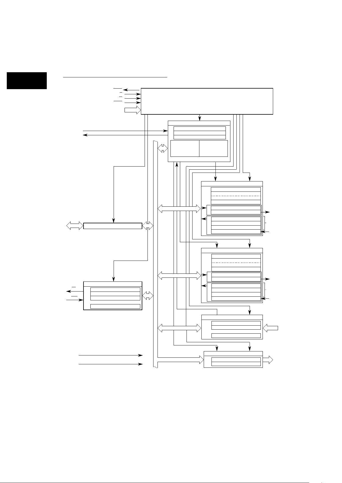
Figure 1-1 is a basic block diagram of the MC68HC681 and should be referred to during the
discussion of its features, which include the following:
• M68000 Bus Compatible
• Two Independent Full-Duplex Asynchronous Receiver/Transmitter Channels
• Maximum Data Transfer Rate:
— 1X — 1 Mbits/second
— 16X — 250 kbits/second
• Quadruple-Buffered Receiver Data Registers
• Double-Buffered Transmitter Data Registers
• Independently Programmable Baud Rate for Each Receiver and Transmitter Selectable
From:
— 18 Fixed Rates: 50 to 38.4k Baud
— One User Defined Rate Derived from a Programmable Timer/Counter
— External 1X Clock or 16X Clock
Page 13
Introduction
1-2
MC68HC681 USER’S MANUAL
MOTOROLA
1
Figure 1-1. MC68HC681 Block Diagram
INTERNAL CONTROL LOGIC
CHANNEL A
RS4-RS1
EXTERNAL
INTERFACE
TxDA
RxDA
X1
X2
PROCESSOR
INTERFACE
V
CC
IRQ
DTACK
R/W
CS
INTERNAL DATA BUS
CRA
COMMAND REGISTER W
MR1A MODE REGISTER
1
R/W
MR2A
MODE REGISTER 2 R/W
SRA STATUS REGISTER
R
THRA TRANSMIT HOLDING REG W
RHRA RECEIVE HOLDING REG (3)
R
RHRA (2)
TBA
RBA
TRANSMIT SHIFT REG
RHRA (1)
RECEIVE SHIFT REGISTER
CHANNEL B
TxDB
RxDB
CRB COMMAND REGISTER
W
MR1B MODE REGISTER 1
R/W
MR2B MODE REGISTER 2 R/W
SRB STATUS REGISTER R
THRB TRANSMIT HOLDING REG
W
RHRB
RECEIVE HOLDING REG (3)
R
RHRB (2)
TBB
RBB
TRANSMIT SHIFT REGISTER
RHRB (1)
RECEIVE SHIFT REGISTER
INPUT PORT
IPCR
INPUT PORT CHANGE REG
R
AUX CONTROL REG (4 BITS) W
ACR
INPUT PORT (6 BITS)
R
ACR
*
Same ACR as in Interrupt Control Logic
*
OUTPUT PORT
OPCR OUTPUT PORT CONFIG REG
W
OUTPUT PORT REG (8 BITS)
W
OPR
FIFO
TIMING LOGIC
Current Count in Counter Mode may be Read
*
INTERRUPT CONTROL LOGIC
IMR INTERRUPT MASK REG W
INTERRUPT STATUS REG R
AUX CONTROL REG (4 BITS) W
ACR
*
Same ACR as in Input Port
*
D7-D0
DATA BUS BUFFER
CSRA CHANNEL A CLOCK SELECT REG W
CHANNEL B CLOCK SELECT REG
W
ACR AUXILIARY CONTROL REG (4 BITS) W
CSRB
COUNTER/TIMER
UPPER REGISTER
(MOST SIGNIF 8 BITS)
W
*
COUNTER/TIMER
LOWER REGISTER
(LEAST SIGNIF 8 BITS)
W
*
ISR
GND
OP7-OP0
RESET
IP5-IP0
INTERRUPT VECTOR REG
R/W
IVR
IACK
FIFO
Page 14

Introduction
MOTOROLA
MC68HC681 USER’S MANUAL
1-3
1
• Programmable Data Format
— Five to eight data bits
— Odd, Even, force parity, or no parity
— One, one and one-half, or two stop bits
• Programmable Channel Modes
— Normal (full duplex)
— Automatic echo
— Local loopback
— Remote loopback
• Automatic Wake-up Mode for Multidrop Applications
• Multifunction 6-Bit Input Port
— Clock or control input functions
— Change-of-state detection on four inputs
• Multifunction 8-Bit Output Port
— Individual bit set/reset capability
— Status/Interrupt signal programmable outputs
• Multifunction 16-Bit Programmable Counter/Timer
• Versatile Interrupt System
— Single interrupt output with eight maskable interrupting conditions
— Interrupt vector output on interrupt acknowledge
— Programmable output port can be configured to provide as many as six separate
wire-ORable interrupt outputs
• Parity, Framing, and Overrun Error Detection
• False-Start Bit Detection
• Line-Break Detection and Generation
• Break Detection starting in the Middle of a Character
• Start-End Break Interrupt/Status
• On-Chip Crystal Oscillator
• TTL Compatible
• Single +5V Power Supply
Page 15

Introduction
1-4
MC68HC681 USER’S MANUAL
MOTOROLA
1
1.1 INTERNAL CONTROL LOGIC
The internal control logic receives operation commands from the central processing unit
(CPU) and generates appropriate signals to the internal sections to control device operation.
The internal control logic allows access to the registers within the DUART and performs
various commands by decoding the four register-select lines (RS1 through RS4). Besides
the four register-select lines, there are three other inputs to the internal control logic from the
CPU: read/write (R/W
), which allows read and write transfers between the CPU and DUART
via the data bus buffer; chip-select (CS
), which is the DUART chip-select; and reset
(RESET
), which initializes or resets the DUART. The data transfer acknowledge (DTACK)
signal, which is asserted during read, write, or interrupt-acknowledge cycles, is the internal
control logic output. The DTACK
signal indicates to the CPU that data has been latched on
a CPU write cycle or that valid data is present on the data bus during a CPU read cycle or
interrupt-acknowledge (IACK
) cycle.
1.2 TIMING LOGIC
The timing logic consists of a crystal oscillator, a baud-rate generator (BRG), a
programmable 16-bit counter/timer (C/T), and four clock selectors. The crystal oscillator
operates directly from a 3.6864 MHz crystal connected across the X1 and X2 inputs or from
an external clock of the appropriate frequency connected to X1. The X1 clock serves as the
basic timing reference for the baud-rate generator, the C/T, and other internal circuits. The
part can operate without an X1 clock but with the following restrictions:
• The X1 input must be connected to GND or V
CC
• The receiver(s) and transmitter(s), if used, must not be programmed to select any of the
18 standard rates generated by the BRG
• The counter/timer, if used, must not be programmed to the X1 or X1/16 selection
• The change-detect on IP0-IP3 will not operate
• DTACK
will not be generated on any bus cycle
The baud-rate generator operates from the X1 clock input and can generate 18 commonly
used data communication baud rates ranging from 50 to 38.4k by producing internal clock
outputs at 16 times the actual baud rate. The C/T can produce a 16X clock for other baud
rates by counting down its programmed clock source. Other baud rates can also be derived
by connecting 16X or 1X clocks to certain input port pins that have alternate functions as
receiver or transmitter clock inputs. Four clock selectors allow the independent selection of
any of these baud rates for each receiver and transmitter. Customers can program the 16bit C/T within the DUART to use one of several clock sources as its input. The output of the
C/T is available to the internal clock selectors and can also be programmed to appear at
parallel output OP3. In the timer mode, the C/T acts as a programmable divider and can
generate a square-wave output at OP3. In the counter mode, the C/T can be started and
stopped under program control. When stopped, the CPU can read its contents. The counter
counts down the number of pulses stored in the concatenation of the C/T upper register and
C/T lower register and produces an interrupt. This is a system-oriented feature that can be
used to record timeouts when implementing various application protocols.
Page 16

Introduction
MOTOROLA
MC68HC681 USER’S MANUAL
1-5
1
1.3 INTERRUPT CONTROL LOGIC
The following registers are associated with the interrupt control logic:
• Interrupt Mask Register (IMR)
• Interrupt Status Register (ISR)
• Auxiliary Control Register (ACR)
• Interrupt Vector Register (IVR)
Refer to Section 4 Programming and Register Descriptions for more complete
information on these registers.
A single active-low interrupt output (IRQ
) can notify the processor that any of eight internal
events has occurred. These eight events are described in the discussion of the interrupt
status register (ISR) in Section 4 Programming and Register Descriptions . Customers
can program the interrupt mask register (IMR) to allow only certain conditions to cause IRQ
to be asserted while the CPU can read the ISR to determine all currently active interrupting
conditions. When an active-low interrupt acknowledge signal (IACK
) from the processor is
asserted while the DUART has an interrupt pending, the DUART will place the contents of
the interrupt vector register (IVR) on the data bus and assert the data transfer acknowledge
signal (DTACK
). If the DUART has no pending interrupt, it ignores IACK cycles. In addition,
customers can program the parallel outputs OP3 through OP7 to provide discrete interrupt
outputs for the transmitters, the receivers, and the C/T.
1.4 DATA BUS BUFFER
The data bus buffer provides the interface between the external and internal data buses. It
is controlled by the internal control logic to allow read and write data transfer operations to
occur between the controlling CPU and DUART by way of the eight parallel data lines (DO
through D7).
1.5 COMMUNICATION CHANNELS A AND B
Each communication channel comprises a full-duplex asynchronous receiver/transmitter
(UART). The operating frequency for each receiver and each transmitter can be selected
independently from the baud-rate generator, the C/T, or from an external clock. The
transmitter accepts parallel data from the CPU, converts it to a serial bit stream, inserts the
appropriate start, stop, and optional parity bits, and outputs a composite serial stream of
data on the TxD output pin. The receiver accepts serial data on the RxD pin, converts this
serial input to parallel format, checks for a start bit, stop bit, parity bit (if any), or break
condition, and transfers an assembled character to the CPU during read operations.
1.6 INPUT PORT
The CPU reads the inputs to this 6-bit port (IP0 through IP5). High or low inputs to the input
port result in the CPU reading a logic one or logic zero, respectively; that is, there is no
inversion of the logic level. Each input port bit also has an alternate control function
capability. The alternate functions can be enabled/disabled on a bit-by-bit basis.
Page 17

Introduction
1-6
MC68HC681 USER’S MANUAL
MOTOROLA
1
Four change-of-state detectors are associated with inputs IP0, IP1, IP2, and IP3. If a highto-low or low-to-high transition occurs on any of these inputs and the new level is stable for
more than 25 to 50 microseconds (best-to-worst case times), the corresponding bit in the
input port change register (IPCR) will be set. The sampling clock of the change detectors is
the X1/96 tap of the baud-rate generator (the 2400 baud tap), which is 38.4kHz if X1 is
3.6864MHz. A new input level must be sampled on two consecutive sample clocks to
produce a change detect. Also, customers can program the DUART to allow a change of
state
to
generate an interrupt to the CPU. The IPCR bits are cleared when the CPU reads
the register.
1.7 OUTPUT PORT
This 8-bit multipurpose output port can be used as a general-purpose output port.
Associated with the output port is an output port register (OPR). All bits of the OPR can be
individually set and reset. A bit is set by performing a write operation at the appropriate
address with the accompanying data specifying the bits to be set (one equals set and zero
equals no change). Similarly, a bit is reset by performing a write operation at another
address with the accompanying data specifying the bits to be reset (one equals reset and
zero equals no change).
The OPR stores data that is to be output at the output port pins. Unlike the input port, if a
particular bit of the OPR is set to a logic one or logic zero, the output pin will be at a low or
high level, respectively. Thus, a logic inversion occurs internal to the DUART with respect
to this register. The outputs are complements of the data contained in the OPR. Table 4-1
and Section 4 Programming and Register Descriptions provide more information on the
address location of the output port register and setting and resetting bits of this register.
Besides general-purpose outputs, the outputs can be individually assigned specific auxiliary
functions serving the communication channels. The assignment is accomplished by
appropriately programming the channel A and B mode registers (MR1A, MR1B, MR2A, and
MR2B) and the output port configuration register (OPCR). Section 4 Programming and
Register Descriptions provides more information on the mode registers and the OPCR.
Page 18
MOTOROLA
MC68HC681 USER’S MANUAL
2-1
2
SECTION 2
SIGNAL DESCRIPTIONS
This section briefly describes the input and output signals. Table 2-1 provides a quick
reference for determining a signal’s pin number, its use as an input or output, whether it is
active high or low, and the section that contains more information about its operation.
NOTE
The terms assertion and negation will be used extensively to
avoid confusion when dealing with a mixture of "active low" and
"active high" signals. The term assert or assertion indicates
that a signal is active or true, independent of whether that level
is represented by a high or low voltage. The term negate or
negation indicates that a signal is inactive or false.
Table 2-1. Signal Summary
SIGNAL NAME MNEMONIC
PIN NO.
IN/OUT
ACTIVE
STATE
REFER TO
PARA. NO.
P PKG. FN PKG.
Power Supply (5 V) V
CC
40 44 In High 2.1
Ground GND 20 22 In Low 2.1
Crystal Input or External Clock X1 32 36 In — 2.2
Crystal Output X2 33 37 Out — 2.3
Reset RESET
34 38 In Low 2.4
Chip Select CS
35 39 In Low 2.5
Read/Write R/W
8 9 In High/Low 2.6
Data Transfer Acknowledge DTACK
9 10 Out
1
Low 2.7
Register-Select Bus Bit 4 RS4 6 7 In High 2.8
Register-Select Bus Bit 3 RS3 5 6 In High 2.8
Register-Select Bus Bit 2 RS2 3 4 In High 2.8
Register-Select Bus Bit 1 RS1 1 2 In High 2.8
Bidirectional-Data Bus Bit 7 D7 19 21 In/Out High 2.9
Bidirectional-Data Bus Bit 6 D6 22 25 In/Out High 2.9
Bidirectional-Data Bus Bit 5 D5 18 20 In/Out High 2.9
Bidirectional-Data Bus Bit 4 D4 23 26 In/Out High 2.9
Bidirectional-Data Bus Bit 3 D3 17 19 In/Out High 2.9
Page 19
Signal Descriptions
2-2
MC68HC681 USER’S MANUAL
MOTOROLA
2
2.1 V
CC
AND GND
Power is supplied to the DUART using these two signals. V
CC
is power ( + 5 volts) and GND
is the ground connection.
2.2 CRYSTAL INPUT OR EXTERNAL CLOCK (X1)
This input is one of two connections to a crystal or a connection to an external CMOS-level
clock. If a crystal is used, a capacitor of approximately 10 to 15 picofarads should be
connected from this pin to ground.
Bidirectional-Data Bus Bit 2 D2 24 27 In/Out High 2.9
Bidirectional-Data Bus Bit 1 D1 16 18 In/Out High 2.9
Bidirectional-Data Bus Bit 0
(Least-Significant Bit)
D0 25 28 In/Out High 2.9
Interrupt Request IRQ
21 24 Out
1
Low 2.10
Interrupt Acknowledge IACK
37 41 In Low 2.11
Channel A Transmitter Serial Data TxDA 30 33 Out — 2.12
Channel A Receiver Serial Data RxDA 31 35 In — 2.13
Channel B Transmitter Serial Data TxDB 11 13 Out — 2.14
Channel B Receiver Serial Data RxDB 10 11 In — 2.15
Parallel Input 5 IP5 38 42 In — 2.16.1
Parallel Input 4 IP4 39 43 In — 2.16.2
Parallel Input 3 IP3 2 3 In — 2.16.3
Parallel Input 2 IP2 36 40 In — 2.16.4
Parallel Input 1 IP1 4 5 In — 2.16.5
Parallel Input 0 IP0 7 8 In — 2.16.6
Parallel Output 7 OP7 15 17 Out
2
— 2.17.1
Parallel Output 6 OP6 26 29 Out
2
— 2.17.2
Parallel Output 5 OP5 14 16 Out
2
— 2.17.3
Parallel Output 4 OP4 27 30 Out
2
— 2.17.4
Parallel Output 3 OP3 13 15 Out
2
— 2.17.5
Parallel Output 2 OP2 28 31 Out — 2.17.6
Parallel Output 1 OP1 12 14 Out — 2.17.7
Parallel Output 0 OP0 29 32 Out — 2.17.8
NOTES:
1. Requires a pullup resistor
2. May require a pullup resistor, depending on its programmed function.
Table 2-1. Signal Summary (Continued)
SIGNAL NAME MNEMONIC
PIN NO.
IN/OUT
ACTIVE
STATE
REFER TO
PARA. NO.
P PKG. FN PKG.
Page 20

Signal Descriptions
MOTOROLA
MC68HC681 USER’S MANUAL
2-3
2
2.3 CRYSTAL INPUT (X2)
This input is an additional connection to a crystal (see Section 2 Signal Descriptions). If an
external CMOS-level clock is used, this pin must be left open. If a crystal is used, a capacitor
of approximately 10 to 15 picofarads should be connected from this pin to ground.
2.4 RESET (RESET)
The DUART can be reset by asserting the RESET
signal or by programming the appropriate
command register. A hardware reset (assertion of RESET
) clears the following registers:
• Status registers A and B (SRA and SRB)
• Interrupt mask register (IMR)
• Interrupt status register (ISR)
• Output port register (OPR)
• Output port configuration register (OPCR)
RESET
performs the following operations:
• Initializes the interrupt vector register (IVR) to 0F
16
• Places parallel outputs OP0 through OP7 in the high state
• Places the counter/timer in timer mode
• Places channels A and B in the inactive state with the transmitter serial-data outputs
(TxDA and TxDB) in the mark (high) state.
Software resets are not as encompassing and are achieved by appropriately programming
the channel A and/or B command registers. Reset commands can be programmed through
the command register to reset the receiver, transmitter, error status, or break-change
interrupts for each channel. Refer to Section 4 Programming and Register Descriptions
for more information.
2.5 CHIP-SELECT (CS)
This active-low input signal, when low, enables data transfers between the CPU and DUART
on the data lines (D0 through D7). These data transfers are controlled by read/write (R/W
)
and the register-select inputs (RS1 through RS4). When chip-select is high, the D0 through
D7 data lines are placed in the high-impedance state.
2.6 READ/WRITE (R/W)
When high, this input indicates a read cycle; when low, it indicates a write cycle. Assertion
of the chip-select input initiates a cycle.
Page 21

Signal Descriptions
2-4
MC68HC681 USER’S MANUAL
MOTOROLA
2
2.7 DATA TRANSFER ACKOWLEDGE (DTACK)
This three-state active low output is asserted in read, write, or interrupt-acknowledge (IACK
)
cycles to indicate the proper transfer of data between the CPU and DUART. If there is no
pending interrupt on an IACK cycle, DTACK
is not asserted. DTACK is an “active rescind”
signal: at the end of a transfer, it drives high momentarily, then is three-stated so that it can
be wire-ANDed with other DTACK
sources, like an open-drain signal.
2.8 REGISTER-SELECT BUS (RS1–RS4)
The register-select bus lines during read/write operations select the DUART internal
registers, ports, or commands.
2.9 DATA BUS (D0–D7)
These bidirectional three-state data lines transfer commands, data, and status between the
CPU and DUART. D0 is the least-significant bit.
2.10 INTERUPT REQUEST (IRQ)
This active-low, open-drain output signals the CPU that one or more of the eight maskable
interrupting conditions are true.
2.11 INTERUPT ACKOWLEDGE (IACK)
This active-low input indicates an interrupt-acknowledge cycle. If there is an interrupt
pending (IRQ
asserted) and this pin is asserted, the DUART responds by placing the
interrupt vector on the data bus and then asserting DTACK
. If there is no interrupt pending
(IRQ
negated), the DUART ignores this pin.
2.12 CHANNEL A/B TRANSMITTER SERIAL-DATA OUTPUT (TxDA/TxDB)
The independent transmitter serial-data outputs for channel A and B transmit the
least-significant bit first. The output is held high (mark condition) when its associated
transmitter is disabled, idle, or operating in the local loopback mode. (‘‘Mark’’ is high and
‘‘space’’ is low.) Data is shifted out from this pin on the falling edge of the programmed clock
source.
2.13 CHANNEL A/B RECEIVER SERIAL-DATA INPUT (RxDA/RxDB)
The independent receiver serial-data inputs for channel A and B receive the least-significant
bit first. Data on these pins is sampled on the rising edge of the programmed clock source.
2.14 PARALLEL INPUTS (IP0–IP5)
The parallel inputs can be used as general-purpose inputs. However, each pin also has an
alternate function(s) described below.
2.14.1 IP0
This input can be used as the channel A clear-to-send active-low input (CTSA
). A change-of-
state detector is also associated with this input.
Page 22

Signal Descriptions
MOTOROLA
MC68HC681 USER’S MANUAL
2-5
2
2.14.2 IP1
This input can be used as the channel B clear-to-send active-low input (CTSB
). A change-of-
state detector is also associated with this input.
2.14.3 IP2
This input can be used as the channel B receiver external clock input (RxCB), or the
counter/timer external clock input. When this input functions as the external clock to the
receiver, the received data is sampled on the rising edge of the clock. A change-of-state
detector is also associated with this input.
2.14.4 IP3
This input can serve as the channel A transmitter external clock input (TxCA). When this
input functions as the external clock to the transmitter, the transmitted data is clocked on the
falling edge of the clock. A change-of-state detector is also associated with this input.
2.14.5 IP4
This input can be used as the channel A receiver external clock input (RxCA). When this
input functions as the external clock to the receiver, the received data is sampled on the
rising edge of the clock.
2.14.6 IP5
This input can serve as the channel B transmitter external clock (TxCB). When this input is
used as the external clock to the transmitter, the transmitted data is clocked on the falling
edge of the clock.
2.15 PARALLEL OUTPUTS (OP0–OP7)
The parallel outputs can be used as general-purpose outputs; however, each pin also has
an alternate function(s), described below.
2.15.1 OP0
This output can function as the channel A transmitter active-low request-to-send (RTSA
)
output, or as the channel A receiver active-low ready-to-receive (RTRA
) output. When used
for RTSA
, it is automatically negated by the transmitter. When used for RTRA, the receiver
automatically negates and reasserts OP0.
2.15.2 OP1
This output can serve as the channel B transmitter active-low request-to-send (RTSB
)
output, or as the channel B receiver active-low ready-to-receive (RTRB
) output. When used
for RTSB
, the transmitter automatically negates OP1 by the transmitter. When used for
RTRB
, the receiver automatically negates and reasserts OP1.
Page 23

Signal Descriptions
2-6
MC68HC681 USER’S MANUAL
MOTOROLA
2
2.15.3 OP2
This output can be used as the channel A transmitter 1X-clock or 16X-clock output or the
channel A receiver 1X-clock output.
2.15.4 OP3
This output can function as the open-drain active-low counter-ready output, the open-drain
timer output, the channel B transmitter 1X-clock output, or the channel B receiver 1X-clock
output.
2.15.5 OP4
This output can serve as the channel A open-drain active-low receiver-ready or buffer-full
interrupt outputs (RxRDYA
/FFULLA) by appropriately programming bit 6 of mode
register 1A.
2.15.6 OP5
This output can be used as the channel B open-drain active-low receiver-ready or buffer-full
interrupt outputs (RxRDYB
/FFULLB) by appropriately programming bit 6 of mode
register 1B.
2.15.7 OP6
This output can function as the channel A open-drain active-low transmitter-ready interrupt
output (TxRDYA
).
2.15.8 OP7
This output can serve as the channel B open-drain active-low transmitter-ready interrupt
output (TxRDYB
).
Page 24

MOTOROLA
MC68HC681 USER’S MANUAL
3-1
3
SECTION 3
OPERATION
3.1 TRANSMITTER
The channel A and B transmitters are enabled for data transmission through their respective
command registers (refer to Section 4 Programming and Register Descriptions ). The
DUART signals the CPU it is ready to accept a character by setting the transmitter-ready bit
in the channel’s status register. Customers can program this condition to generate an
interrupt request on the IRQ
output, an interrupt request for channel A’s transmitter on
parallel output OP6, or for channel B’s transmitter on parallel output OP7. When a character
is loaded into the transmit buffer (TB), the above conditions for the respective channel are
negated. Data is transferred from the transmit holding register to the transmit shift register
when the shift register is idle or has completed transmission of the previous character. The
transmitter ready conditions are then re-asserted, providing one full character time of
buffering. Characters cannot be loaded into the transmit buffer while the transmitter is
disabled.
The transmitter converts the parallel data from the CPU to a serial bit stream on the
transmitter serial-data output pin. It automatically sends a start bit followed by the
programmed number of data bits, an optional parity bit, and the programmed number of stop
bits. The least-significant bit is sent first. Data is shifted out the transmit serial data output
pin on the failing edge of the programmed clock source. After the transmission of the stop
bits, if a new character is not available in the transmit holding register the transmitter
serial-data output remains high and the transmitter-empty bit in the status register (SRA and
SRB) will be set to a one. Transmission resumes and the transmitter-empty bit is cleared
when the CPU loads a new character into the transmit buffer (TBA or TBB). If the transmitter
receives a disable command, it will continue operating until the character in the transmit shift
register is completely sent out. Another character in the holding register is not sent but is not
discarded; it will be sent when the transmitter is re-enabled. The transmitter can be reset
through a software command (refer to Section 2.4 RESET ). If it is reset, operation ceases
immediately and must be enabled through the command register before resuming
operation. Reset also discards any character in the holding register.
If clear-to-send (CTS
) operation is enabled, the CTS input (alternate function of IP0 or IP1)
must be low in order for the character to be transmitted. If it goes high in the middle of a
transmission, the character in the shift register is transmitted and TxD then remains in the
marking state until CTS
again goes low. The transmitter can also be forced to send a
continuous low condition by issuing a send-break command. The state of CTS
is ignored by
the transmitter when it is to send a break.
Page 25

Operation
3-2
MC68HC681 USER’S MANUAL
MOTOROLA
3
A send-break is deferred as long as the transmitter has characters to send, but if normal
character transmission is inhibited by CTS
, the send-break will proceed. The send-break
must be terminated by a stop-break, disable, or reset before normal character transmission
can resume.
Customers can program the transmitter to automatically negate the request-to-send (RTS)
output (alternate function of OP0 and OP1) on completion of a message transmission. If the
transmitter is programmed to operate in this manner, the RTS
output must be manually
asserted before each message is transmitted. If OP0 (or OP1) is programmed in automatic
RTS mode, the RTS
output will be automatically negated when the transmitter is disabled
and the transmit-shift register and holding register are both empty. In automatic RTS mode,
a character in the holding register is not held back by a disable, but no more characters can
be written to the holding register after the transmitter is disabled.
3.2 RECEIVER
The channel A and B receivers are enabled for data reception through the respective
channel’s command register. The channel’s receiver looks for the high-to-low (mark-tospace) transition of a start bit on the receiver serial-data input pin. If operating in 16X clock
mode, the serial input data is re-sampled on the next 7 clocks. If the receiver serial data is
sampled high, the start bit is invalid and the search for a valid start bit begins again. If
receiver serial data is still low, a valid start bit is assumed and the receiver continues to
sample the input at one bit time intervals (at the theoretical center of the bit) until the proper
number of data bits and the parity bit (if any) have been assembled and one stop bit has
been detected. Data on the receiver serial data input pin is sampled on the rising edge of
the programmed clock source.
During this process, the least-significant bit is received first. The data is then transferred to
a receive holding register (RHR) and the receiver-ready bit in the status register (SRA or
SRB) is set to a one (see Figure 3-1). This condition can be programmed to generate an
interrupt request on the IRQ
output, an interrupt request for channel A’s receiver on parallel
output OP4, or an interrupt request for channel B’s receiver on parallel output OP5. If the
character length is less than eight bits, the most significant unused bits in the receive holding
register (RHR) are set to zero.
If the stop bit is sampled as a 1, the receiver will immediately look for the next start bit.
However, if the stop bit is sampled as a 0, either a framing error or a received break has
occurred. If the stop bit is 0 and the data and parity (if any) are not all zero, it is a framing
error; the damaged character is transferred to a holding register with the framing error flag
set. If the receiver serial data remains low for one-half of the bit period after the stop bit was
sampled, the receiver operates as if a new start bit transition has been detected. If the stop
bit is 0 and the data and parity (if any) are also all zero, it is a break. A character consisting
of all zeros will be loaded into a receive holding register (RHR) with the received-break bit
(but not the framing error bit) set to a one. The receiver serial-data input must return to a
high condition for at least one-half bit time before a search for the next start bit begins.
Page 26

Operation
MOTOROLA
MC68HC681 USER’S MANUAL
3-3
3
The receiver can detect a break that starts in the middle of a character provided the break
persists completely through the next character time or longer. When the break begins in the
middle of a character, the receiver will place the damaged character in a holding register
with the framing error bit set. Then, provided the break persists through the next character
time, the receiver will also place an all-zero character in the next holding register with the
received-break bit set.
The parity error, framing error, overrun error, and received-break conditions (if any) set error
and break flags in the status register at the received character boundary and are valid only
when the receiver-ready bit (RxRDY) in the status register is set. A first-in first-out (FIFO)
stack is used in each channel’s receive buffer logic and consists of three receive holding
registers. The receiver buffer (RBA or RBB) is composed of the FIFO and a receive shift
register connected to the receiver serial-data input. Data is assembled in the shift register
and loaded into the top-most empty FIFO receive holding register position. Thus, data
flowing from the receiver to the CPU is quadruply buffered.
The receiver-ready bit in the status register (SRA or SRB) is set whenever one or more
characters are available to be read. A read of the receiver buffer produces an output of data
from the top of the FIFO stack. After the read cycle, the data at the top of the FIFO stack and
its associated status bits are "popped" and new data can be added at the bottom of the stack
by the receive shift register. The FIFO-full status bit is set if all three stack positions are filled
with data. Either the receiver-ready or the FIFO-full status bits can be selected to cause an
interrupt. In addition to the data byte, three status bits (parity error, framing error, and
received break) are appended to each data character in the FIFO (overrun is not). By
programming the error-mode control bit in the channel’s mode register, status can be
provided for "character" or "block" modes.
In the "character" mode, the status register (SRA or SRB) is updated on a character-bycharacter basis and applies only to the character at the top of the FIFO. Thus, the status
must be read before the character is read. Reading the character pops it and its error flags
off the FIFO.
In the "block" mode, the status provided in the status register for the parity error, framing
error, and received-break conditions is the logical OR of these respective bits for all
characters coming to the top of the FIFO stack since the last reset error command was
issued. That is, beginning at the last reset-error command issued, a continuous logical-OR
function of corresponding status bits is produced in the status register as each character
comes to the top of the FIFO stack.
The block mode is useful in applications requiring the exchange of blocks of information
where the software overhead of checking each character’s error flags cannot be tolerated.
In this mode, entire messages can be received and only one data integrity check is
performed at the end of each message. Although data reception in this manner has speed
advantages, there are also disadvantages. Because each character is not individually
checked for error conditions by the software, if an error occurs within a message the error
will not be recognized until the final check is performed. Also, there is no indication of which
character(s) is in error within the message.
Page 27

Operation
3-4
MC68HC681 USER’S MANUAL
MOTOROLA
3
The block mode can only be used if either (or both) of two conditions can be guaranteed:
1. The length of the block is known before the last character of the block is read, so that
the block error status can be read and cleared before reading the last character;
2. There will never be another character already present in the FIFO until the last character of the message is read (leaving the FIFO empty), the status is read, and a reset
error command is issued. Otherwise, errors in the first character of the next block could
be reported erroneously on the current block, or they could be prematurely cleared and
not reported in the error status of the next block.
In either mode, reading the status register (SR) does not affect the FIFO. The FIFO is
"popped" only when the receive buffer (RBA or RBB) is read. If all three of the FIFO’s receive
holding registers are full when a new character is received, that character is held in the
receive shift register until a FIFO position is available. If an additional character is received
while this state exists, the contents of the FIFO are not affected, but the character previously
in the shift register is lost and the overrun-error status bit will be set upon receipt of the start
bit of the new overrunning character.
To support flow control, a receiver can automatically negate and reassert the ready-toreceive (RT
R) output (alternate function of parallel outputs OP0 and OP1). The RTS and
RTR
functions both use OP0 (channel A) and/or OP1 (channel B). Both functions should not
be enabled for the same channel at the same time. If programmed to operate in this mode,
the ready-to-receive output will automatically be negated by the receiver when a valid start
bit is received and the FIFO stack is full. When a FIFO position becomes available, the
ready-to-receive output will be reasserted automatically by the receiver. Connecting the
ready-to-receive output to the clear-to-send (CTS
) input of a transmitting device, prevents
overrun errors in the receiver. The RT
R output must be manually asserted the first time.
Thereafter, the receiver will control the RT
R output.
If the FIFO stack contains characters and the receiver is then disabled, the characters in the
stack can still be read but no additional characters can be received until the receiver is again
enabled. If the receiver is disabled while receiving a character, or while there is a character
in the shift register waiting for a FIFO opening, these characters are lost. If the receiver is
reset, the FIFO stack and all of the receiver status bits, the corresponding output ports, and
the interrupt request are reset. No additional characters can be received until the receiver is
again enabled.
3.3 LOOPING MODES
Besides the normal operation mode in which the receiver and transmitter operate
independently, each DUART channel can be configured to operate in various looping modes
that are useful for local and remote system diagnostic functions. These modes are described
in the following paragraphs with additional information available in Section 4 Programming
and Register Descriptions .
Page 28

Operation
MOTOROLA
MC68HC681 USER’S MANUAL
3-5
3
3.3.1 Automatic-Echo Mode
In this mode, the channel automatically retransmits the received data on a bit-by-bit basis.
The local CPU-to-receiver communication continues normally but the CPU-to-transmitter
link is disabled.
3.3.2 Local-Loopback Mode
In this mode, the transmitter output is internally connected to the receiver input. The external
TxD pin is held in the mark (high) state in this mode. This mode is useful for testing the
operation of a local DUART channel. By sending data to the transmitter and checking that
the data assembled by the receiver is the same data that was sent, proper channel operation
can be assured. In this mode the CPU-to-transmitter and CPU-to-receiver communications
continue normally.
3.3.3 Remote-Loopback Mode
In this mode, the channel automatically retransmits the received data on a bit-by-bit basis.
The local CPU-to-receiver and CPU-to-transmitter links are disabled. This mode is useful in
testing the receiver and transmitter operation of a remote channel. This mode requires the
remote channel receiver to be enabled.
3.4 MULTIDROP MODE
Customers can program the channel to operate in a wake-up mode for multidrop
applications. This mode is selected by setting bits three and four in mode register one
(MR1). In this mode of operation, a master station’s channel, connected to several slave
stations (a maximum of 256 unique slave stations), transmits an address character followed
by a block of data characters targeted for one or more of the slave stations. In this mode,
the channel receivers within the slave stations are disabled, but they continuously monitor
the data stream sent out from the master station. When the slave station’s channel receivers
detect any address character in the data stream, each receiver notifies its respective CPU
by setting receiver ready (RxRDY) and generating an interrupt, if programmed to do so.
Each slave station CPU then compares the received address to its station address and
enables its receiver if it wants to receive the subsequent data from the master station. Slave
stations that are not addressed continue monitoring the data stream for the next address
character. An address character flags the end of one block of data and the start of another.
After receiving a block of data, the slave station’s CPU may disable the channel receiver and
re-initiate the process.
A transmitted character from the master station consists of a start bit, the programmed
number of data bits, an address/data (A/D) bit flag, and the programmed number of stop bits.
The address/data bit identifies to the slave station’s channel whether the character should
be interpreted as an address character or a data character. The character is interpreted as
an address character if the A/D bit is set to a one or interpreted as a data character if it is
set to a zero. The polarity of the transmitted address/data bit is selected by programming bit
two in mode register one (MR1) to a one for an address character and to a zero for data
characters. Customers should program the mode register prior to loading the corresponding
data or address characters into the transmit buffer (TBA or TBB).
Page 29

Operation
3-6
MC68HC681 USER’S MANUAL
MOTOROLA
3
In the multidrop mode, the receiver continuously monitors the received data stream
regardless of whether it is enabled or disabled. If the receiver is disabled, it sets the receiver
ready status bit and loads the character into the FIFO receive holding register stack provided
the received address/data bit is a one (address tag). The received character is discarded if
the received address/data bit is a zero (data tag). If the receiver is enabled, all received
characters are transferred to the CPU by way of the receive holding register stack during
read operations. In either case, the data bits are loaded into the data portion of the FIFO
stack while the address/data bit is loaded into the status portion of the FIFO stack normally
used for parity error (status register bit five). Framing error, overrun error, and breakdetection operate normally regardless of whether the receiver is enabled or disabled.
The address/data bit takes the place of the parity bit and parity is neither calculated nor
checked for characters in this mode. Nevertheless, messages in this mode can still contain
error detection and correction information. One way to provide error detection (if 8-bit
characters are not required) would be to use software to calculate parity and append it to 5-,
6-, or 7-bit characters. Another way to provide error detection for the entire message would
be to use cyclic redundancy checks, or Hamming codes similar to those used in
synchronous protocols, perform the check in software, and append the check character(s)
to the end of the message.
3.5 COUNTER/TIMER
The 16-bit counter/timer (C/T) can operate in a counter mode or a timer mode. In either
mode, customers can program the C/T input (clock source) to come from several sources
and program the C/T output to appear on output port pin OP3. The value (preload value)
stored in the concatenation of the C/T upper register (CTUR) and the C/T lower register
(CTLR) can be from 0001
16
through FFFF
16
and can be changed at any time. In counter
mode, the CPU can start and stop the C/T. This mode allows the C/T to function as a system
stopwatch, a real-time single interrupt generator, or a device watchdog. In timer mode, the
C/T runs continuously; the CPU cannot start or stop it. Instead, the CPU only resets the
C/T interrupt. This mode allows the C/T to be used as a programmable clock source for
channels A and B, or periodic interrupt generator. At power-up and after reset, the C/T
operates in timer mode.
3.5.1 Counter Mode
In counter mode, the C/T counts down from the preload value using the programmed
counter clock source. The counter clock source can be the channel A transmitter clock, the
channel B transmitter clock, the external clock on the X1 pin divided by sixteen, or an
external clock on the input port pin IP2. The CPU can start and stop the counter, and can
read the count value (CUR:CLR) if the counter is stopped. When a read at the start counter
command address is performed, the counter is initialized to the preload value and begins a
countdown sequence. When the counter counts from 0001
16
to 0000
16
(terminal count), the
C/T-ready bit in the interrupt status register (ISR[3]) is set.
Page 30

Operation
MOTOROLA
MC68HC681 USER’S MANUAL
3-7
3
Customers can program the counter to generate an interrupt request for this condition on
the IRQ
output or output pin OP3. After 0000
16
the counter counts to FFFF
16
, and continues
counting down from there. If the CPU changes the preload value, the counter will not
recognize the new value until it receives the next start counter command (and is
reinitialized). When a read at the stop counter command address is performed, the counter
stops the countdown sequence and clears ISR[3]. The count value should only be read while
the counter is stopped because only one of the count registers (either CUR or CLR) can be
read at a time. If the counter is running, a decrement of CLR that requires a borrow from the
CUR could take place between the two reads.
3.5.2 Timer Mode
In timer mode, the C/T generates a square-wave output derived from the programmed timer
input (clock source). The timer clock source can be the external clock on the X1 input pin
divided by one or sixteen, or it can be an external input on input port pin IP2 divided by one
or sixteen. The square wave generated by the timer has a period of 2x (preload value) x
(period of clock source), is available as a clock source for both communications channels
and can be programmed to appear on output pin OP3. The timer runs continuously; the CPU
cannot stop it. Because the timer cannot be stopped, the count value (CUR:CLR) should not
be read. When a read at the start counter command address is performed, the timer
terminates the current countdown sequence, sets its output to 1 (appears uninverted at
OP3), is initialized to the preload value, and begins a new countdown sequence. When the
counter counts from 0001
16
(terminal count), it inverts its output, is re-initialized to the
preload value and repeats the countdown sequence. After reaching terminal count a second
time, the timer sets the C/T-ready bit in the interrupt status register (ISR[3]), inverts its
output, is re-initialized again, and begins a new countdown sequence. Customers can
program the timer to generate an interrupt request for this condition (every second
countdown cycle) on the IRQ
output. If the CPU changes the preload value, the timer will
not recognize the new value until either (a) it reaches the next terminal count and is
reinitialized automatically, or (b) it is forced to re-initialize by a start command. When a read
at the stop counter command address is performed, the timer clears ISR[3] but does not
stop. Because in timer mode the C/T runs continuously, it should be completely configured
(preload value loaded and start counter command issued) before programming the timer
output to appear on OP3.
Page 31

MOTOROLA
MC68HC681 USER’S MANUAL
4-1
4
SECTION 4
PROGRAMMING AND REGISTER DESCRIPTIONS
4.1 PROGRAMMING DESCRIPTIONS
Customers program the DUART by writing control words into the appropriate registers. The
status registers provide operational feedback that the CPU reads. Table 4-1 describes the
DUART register address and address-triggered commands.
Figure 4-1 illustrates a block diagram of the DUART from a programming perspective and
details the register configuration for each block. Table 4-1 and Figure 4-1 should be referred
to during the discussion of the programming features of the DUART.
Page 32

Programming and Register Descriptions
4-2
MC68HC681 USER’S MANUAL
MOTOROLA
4
Figure 4-1. Programming Block Diagram
INTERNAL CONTROL LOGIC
CHANNEL A
RS4-RS1
EXTERNAL
INTERFACE
TxDA
RxDA
X1
X2
PROCESSOR
INTERFACE
V
CC
IRQ
DTACK
R/W
CS
INTERNAL DATA BUS
CRA
COMMAND REGISTER W
MR1A MODE REGISTER
1
R/W
MR2A
MODE REGISTER 2 R/W
SRA STATUS REGISTER
R
THRA TRANSMIT HOLDING REG W
RHRA RECEIVE HOLDING REG (3)
R
RHRA (2)
TBA
RBA
TRANSMIT SHIFT REG
RHRA (1)
RECEIVE SHIFT REGISTER
CHANNEL B
TxDB
RxDB
CRB COMMAND REGISTER
W
MR1B MODE REGISTER 1
R/W
MR2B MODE REGISTER 2 R/W
SRB STATUS REGISTER R
THRB TRANSMIT HOLDING REG
W
RHRB
RECEIVE HOLDING REG (3)
R
RHRB (2)
TBB
RBB
TRANSMIT SHIFT REGISTER
RHRB (1)
RECEIVE SHIFT REGISTER
INPUT PORT
IPCR
INPUT PORT CHANGE REG
R
AUX CONTROL REG (4 BITS) W
ACR
INPUT PORT (6 BITS)
R
ACR
*
Same ACR as in Interrupt Control Logic
*
OUTPUT PORT
OPCR OUTPUT PORT CONFIG REG
W
OUTPUT PORT REG (8 BITS)
W
OPR
FIFO
TIMING LOGIC
Current Count in Counter Mode may be Read
*
INTERRUPT CONTROL LOGIC
IMR INTERRUPT MASK REG W
INTERRUPT STATUS REG R
AUX CONTROL REG (4 BITS) W
ACR
*
Same ACR as in Input Port
*
D7-D0
DATA BUS BUFFER
CSRA CHANNEL A CLOCK SELECT REG W
CHANNEL B CLOCK SELECT REG
W
ACR AUXILIARY CONTROL REG (4 BITS) W
CSRB
COUNTER/TIMER
UPPER REGISTER
(MOST SIGNIF 8 BITS)
W
*
COUNTER/TIMER
LOWER REGISTER
(LEAST SIGNIF 8 BITS)
W
*
ISR
GND
OP7-OP0
RESET
IP5-IP0
INTERRUPT VECTOR REG
R/W
IVR
IACK
FIFO
Page 33

Programming and Register Descriptions
MOTOROLA
MC68HC681 USER’S MANUAL
4-3
4
Table 4-2 summarizes the various input port pin functions.
Table 4-1. Register Addressing and Address-Triggered Commands
RS4 RS3 RS2 RS1 READ (R/W
= 1) WRITE (R/W = 0)
0000Mode Register A (MR1A, MR2A) Mode Register A (MR1A, MR2A)
0001Status Register A (SRA) Clock-Select Register A (CSRA)
0010Clock-Select Register A
1
(CSRA) Command Register A (CRA)
0011Receiver Buffer A (RBA) Transmitter Buffer A (TBA)
0100Input Port Change Register (IPCR) Auxiliary Control Register (ACR)
0101Interrupt Status Register (ISR) Interrupt Mask Register (IMR)
0110Counter Mode: Current MSB of Counter (CUR) Counter/Timer Upper Register (CTUR)
0111Counter Mode: Current LSB of Counter (CLR) Counter/ Timer Lower Register (CTLR)
1000Mode Register B (MR1B, MR2B) Mode Register B (MR1B, MR2B)
1001Status Register B (SRB) Clock-Select Register B (CSRB)
1010Clock-Select Register B
2
(CSRB) Command Register B (CRB)
1011Receiver Buffer B (RBB) Transmitter Buffer B (TBB)
1100Interrupt-Vector Register (IVR) Interrupt-Vector Register (IVR)
1101Input Port (IP) Output Port Configuration Register (OPCR)
1110Start-Counter Command
3
Output Port
Register (OPR)
Bit Set Command
3
1111Stop-Counter Command
3
Bit Reset Command
3
NOTES:
1. Reading From This Address Is Prohibited In The MC68681.
2. Address Triggered Commands.
Table 4-2. Programming of Input Port Functions
FUNCTION
INPUT PORT PIN
IP5 IP4 IP3 IP2 IP1 IP0
General Purpose Default* Default* Default* Default* Default* Default*
Change-of-State
Detector
No No Yes Yes Yes Yes
External Counter
1X Clock Input
ACR[6:4] = 000
External Timer
16X Clock Input
ACR[6:4] = 100
External Timer
1X Clock Input
ACR[6:4] = 101
Page 34

Programming and Register Descriptions
4-4
MC68HC681 USER’S MANUAL
MOTOROLA
4
Table 4-3 summarizes the various output port pin functions.
RxCA 16X CSRA[7:4] =
1110
RxCA 1X CSRA[7:4] =
1111
TxCA 16X CSRA[3:0] =
1110
TxCA 1X CSRA[3:0] =
1111
RxCB 16X CSRB[7:4] =
1110
RxCB 1X CSRB[7:4] =
1111
TxCB 16X CSAB[3:0] =
1110
TxCB 1X CSRB[3:0] =
1111
TxCTSA MR2A[4] = 1
TxCTSB MR2B[4] = 1
NOTE:
The pin is in this mode unless program med to operate in another mode.
Table 4-3. Programming of Output Port Functions
FUNCTION
OUTPUT PORT PIN
OP7 OP6 OP5 OP4 OP3 OP2 OP1 OP0
General
Purpose
OPCR[7] = 0 OPCR[6] = 0 61PCR[5] = 0 OPCR[4] = 0 OPCR[3:2] = 00 OPCR[1:0] = 00 MR1B[7] = 0
MR2B[5] = 0
MR1B[7] = 0
MR2A[5] = 0
CTRDY OPCR[3:2] = 01,
ACR[6] = 0*
Timer Output OPCR[3:2] = 01,
ACR[6] = 1*
TxCB 1X OPCR[3:2] = 10
RxCB OPCR[3:2] = 11
TxCA 16X OPCR[1:0] = 01
TxCA 1X OPCR[1:0] = 10
RxCA 1X OPCR[1:0] = 11
Table 4-2. Programming of Input Port Functions (Continued)
FUNCTION
INPUT PORT PIN
IP5 IP4 IP3 IP2 IP1 IP0
Page 35

Programming and Register Descriptions
MOTOROLA
MC68HC681 USER’S MANUAL
4-5
4
Table 4-4 summarizes the various clock sources that can be selected for the counter/
timer.
Customers should use caution if the contents of a register are changed during receiver/
transmitter operation as certain changes can produce undesired results. For example,
changing the number of bits per character while the transmitter is active can transmit an
incorrect character. The contents of the clock-select register (CSR) and bit 7 of the
auxiliary control register (ACR[7]) should only be changed after the receiver(s) and
transmitter(s) have been issued software Rx and Tx reset commands. Most bits of the
mode registers should not be changed during receiver/transmitter operation, except that
in multidrop parity mode, the address/data parity type bit can be changed at any time.
TxRDYA
OPCR[6] = 1*
TxRDYB
OPCR[7] = 1*
RxRDYA
OPCR[4] = 1
MR1A[6] = 0*
RxRDYB
OPCR[5] = 1
MR1B[6] = 0*
FFULLA
OPCR[4] = 1,
MR1A[6] = 1*
FFULLB
OPCR[5] = 1
MR1B[6] = 1*
RxRTRA
MR1A[7] = 1
TxRTSA
MR2A[5] = 1
RxRTRB
MR1B[7] = 1
TxRTSB
MR2B[5] = 1
NOTE:
The pin requires a pull-up resistor.
Table 4-4. Selection of Clock Sources for the Counter/Timer
ACR[6] = 0 (COUNTER MODE) ACR[6] = 1 (TIMER MODE)
COUNTER MODE CLOCK SOURCES ACR[5:4] = TIMER MODE CLOCK SOURCES ACR[5:4] =
Input Port Pin IP2 00 Input Port Pin IP2 00
Channel A 1X Transmitter Clock TxCA 01 Input Port Pin IP2 Divided by 16 01
Channel B 1X Transmitter Clock TxCB 10 Crystal/Clock X1 10
Crystal/Clock X1 Divided by 16 11 Crystal/Clock X1 Divided by 16 11
Table 4-3. Programming of Output Port Functions (Continued)
FUNCTION
OUTPUT PORT PIN
OP7 OP6 OP5 OP4 OP3 OP2 OP1 OP0
Page 36

Programming and Register Descriptions
4-6
MC68HC681 USER’S MANUAL
MOTOROLA
4
Similarly, certain changes to the auxiliary control register (ACR bits six through four)
should only be made while the counter/timer (C/T) is not used (i.e., stopped if in counter
mode, output and/or interrupt masked in timer mode).
Channel A mode registers MR1A and MR2A are accessed via an auxiliary pointer. The
pointer is set to mode register one (MR1A) by RESET
or by issuing a "reset pointer"
command via the channel A command register. Any read or write of the mode register
switches the pointer to mode register two (MR2A). All subsequent accesses will address
MR2A unless the pointer is reset to MR1A as described above. The channel B mode
registers MR1B and MR2B are accessed by an identical pointer independent of the
channel A pointer. Mode, command, clock-select, and status registers are duplicated for
each channel to allow independent operation and control (except that both channels are
restricted to baud rates that are in the same set).
4.2 REGISTER BIT FORMATS
Rx RTR—Control
0 = Disabled
1 = Enabled
Rx IRQ = Select
0 = RxRDY
1 = FFULL
Error Mode
0 = Character
1 = Block
Parity Mode (Bits 4 and 3)
0 0 = With Parity
0 1 = Force Parity
1 0 = No Parity
1 1 = Multidrop Mode
Parity Type
With Parity
0 = Even
1 = Odd
Channel A/B Mode Register 1 (MR1A/MR1B)
7 654321 0
RX RTR RX IRQ
ERROR
MODE
PARITY MODE
PARITY
TYPE
BITS PER CHARACTER
Page 37

Programming and Register Descriptions
MOTOROLA
MC68HC681 USER’S MANUAL
4-7
4
Force Parity
0 = Low
1 = High
Multidrop Mode
0 = Data
1 = Address
Bits-per-Character (Bits 1 and 0)
0 0 = 5
0 1 = 6
1 0 = 7
1 1 = 8
Channel Mode (Bits 7 and 6)
0 0 = Normal
0 1 = Automatic Echo
1 0 = Local Loopback
1 1 = Remote Loopback
Tx RTS—Control
0 = Disabled
1 = Enabled
CTS—Enable Transmitter
0 = Disabled
1 = Enabled
Stop Bit Length (Bits 3, 2)
0 0 = 1 Stop Bit
0 1 = 1 Stop Bit
1 0 = 1.5 Stop Bits (Async mode); 2 Stop Bits (Sync mode)
1 1 = 2 Stop Bits
Channel A Mode Register 2 (MR2A/MR2B)
76543210
CHANNEL MODE TX RTS CTS STOP BIT LENGTH UNUSED
Clock-Select Register A/B (CSRA/CSRB)
76543210
RECEIVER-CLOCK SELECT TRANSMITTER CLOCK SELECT
Page 38

Programming and Register Descriptions
4-8
MC68HC681 USER’S MANUAL
MOTOROLA
4
Receiver (Bits 7-4) And Transmitter (Bits 3-0) Clock Selec
t
All clock selects are 16X (async) except code 1111.
Ch A Tx uses IP3
Ch A Rx uses IP4
Ch B Tx uses IP5
Ch B Rx uses IP2
BIT 7 BIT 6 BIT 5 BIT 4 SET 1 SET 2
0000 50 75
0001 110 110
0010 134.5 134.5
0011 200 150
0100 300 300
0101 600 600
0110 1200 1200
0111 1050 2000
1000 2400 2400
1001 4800 4800
1010 7200 1800
1011 9600 9600
1100 38.4K 19.2K
1101 Timer Timer
1110 IPn-16X IPn-16X
1111 IPn-1X IPn-1X
Channel A/B Command Register (CRA/CRB)
76543210
X MISCELLANEOUS COMMANDS
TRANSMITTER
COMMANDS
RECEIVER COMMANDS
Page 39

Programming and Register Descriptions
MOTOROLA
MC68HC681 USER’S MANUAL
4-9
4
X—Not Used, may be set to either 0 or 1
Miscellaneous Commands (Bits 6, 5, 4)
0 0 0 = No Command
0 0 1 = Reset MR Pointer to MR1
0 1 0 = Reset Receiver
0 1 1 = Reset Transmitter
1 0 0 = Reset Error Status
1 0 1 = Reset Channel’s Break-Change Interrupt
1 1 0 = Start Break
1 1 1 = Stop Break
Transmitter Commands (Bits 3 and 2)
0 0 = No Action, Stays in Present Mode
0 1 = Transmitter Enabled
1 0 = Transmitter Disabled
1 1 = Don’t Use, Indeterminate
Receiver Commands (Bits 1 and 0)
0 0 = No Action, Stays in Present Mode
0 1 = Receiver Enabled
1 0 = Receiver Disabled
1 1 = Don’t Use, Indeterminate
These status bits are appended to the corresponding data character in the receive FIFO and are valid only when the RxRDY bit
is set. A read of the status register provides these bits (seven through five) from the top of the FIFO together with bits four through
zero. These bits are cleared by a reset error status command. In character mode, they are discarded when the corresponding
data character is read from the FIFO.
All Bits
0 = No
1 = Yes
Channel A/B Status Register (SRA/SRB)
7*6*5*43210
RECEIVED
BREAK
FRAMING
ERROR
PARITY
ERROR
OVERRUN
ERROR TXEMT TXRDY FFULL RXRDY
Output Port Configuration Register (OPCR)
76543210
OP7 OP6 OP5 OP4 OP3 OP2
Page 40

Programming and Register Descriptions
4-10
MC68HC681 USER’S MANUAL
MOTOROLA
4
OP7
0 = OPR Bit 7
1 = TxRDYB
OP6
0 = OPR Bit 6
1 = TxRDYA
OP5
0 = OPR Bit 5
1 = RxRDYB/FFULLB
OP4
0 = OPR Bit 4
1 = RxRDYA/FFULLA
OP3 (Bits 3 and 2)
0 0 = OPR Bit 2
0 1 = C/T Output
1
1 0 = TxCB (1X)
1 1 = TxCB (1X)
OP2 (Bits 1 and 0)
0 0 = OPR Bit 2
0 1 = TxCA (16X)
1 0 = TxCA (1X)
1 1 = RxCA (1X)
Alternate functions of OP1 and OP0 (TxRTS, RxRTR) are controlled by the mode
registers, not the OPCR. MR1A[7] and MR2A[5] control OP0; MR1B[7] and MR2B[5]
control OP1.
All bits, unless programmed for alternate function
0 = Pin driven high
1 = Pin driven low
1.
If OP3 is to be used for the timer output, customers should program the counter/timer for timer mode
(ACR[6] = 1), initialize the counter/timer preload registers (CTUR and CTLR), and the start counter
command issued before setting OPCR[3:2] = 01.
Output Port Register (OPR)
76543210
OPR7 OPR6 OPR5 OPR4 OPR3 OPR2 OPR1 OPR0
Page 41

Programming and Register Descriptions
MOTOROLA
MC68HC681 USER’S MANUAL
4-11
4
BRG Set Select. Should only be changed after both channels have been reset and are
disabled.
0 = Set 1
1 = Set 2
Counter/Timer—Mode and Clock Source. Should only be altered while the C/T is not in
use (i.e., stopped if in counter mode, output and/or interrupt masked if in timer mode).
Mode Clock Source
0 0 0 Counter External (IP2)
0 0 1Counter TxCA—1X Clock of Channel A Transmitter
0 1 0Counter TxCB—1X Clock of Channel B Transmitter
0 1 1Counter Crystal or External Clock (X1/Clk) Divided by 16
1 0 0Timer External (IP2)
1 0 1Timer External (IP2) Divided by 16*
1 1 0 Timer Crystal or External Clock (X1/Clk)
1 1 1Timer Crystal or External Clock (X1/Clk) Divided by 16
IP Change-Of-State Visible in ISR (Bits 3, 2, 1, 0)
0 = Disabled
1 = Enabled
IP Delta (Change-of-state) (Bits 7,6,5,4).
0 = No
1 = Yes
IP Level (Bits 3,2,1,0).
0 = Low
1 = High
Auxiliary Control Register (ACR)
76543210
BRG SET
SELECT
COUNTER/TIMER
IP3
CHANGE
VISIBLE IN
ISR
IP2
CHANGE
VISIBLE IN
ISR
IP1
CHANGE
VISIBLE IN
ISR
IP0
CHANGE
VISIBLE IN
ISR
Input Port Change Register (IPCR)
76543210
IP3 DELTA IP2 DELTA IP1 DELTA IP0 DELTA IP3 LEVEL IP2 LEVEL IP1 LEVEL IP0 LEVEL
Page 42

Programming and Register Descriptions
4-12
MC68HC681 USER’S MANUAL
MOTOROLA
4
All Bits
0 = This interrupt source is not active
1 = This interrupt source is active
All Bits
0 = Mask this interrupt source
1 = Allow this interrupt source to assert IRQ
* Bit seven has no external pin. Upon reading the input port, bit seven will always be
read as a one
† Bit six has no external pin. Upon reading the input port, bit six will reflect the current
logic level of IACK
Interrupt Status Register (ISR)
76543210
INPUT PORT
CHANGE
DELTA
BREAK B
RXRDYB/
FFULLB
TXRDYB
COUNTER/
TIMER
READY
DELTA
BREAK A
RXRDYA/
FFULLA
TXRDYA
Interrupt Mask Register (IMR)
76543210
INPUT PORT
CHANGE
DELTA
BREAK B
RXRDYB/
FFULLB
TXRDYB
COUNTER/
TIMER
READY
DELTA
BREAK A
RXRDYA/
FFULLA
TXRDYA
Counter/Timer Upper Register (CTUR)
76543210
C/T[15] C/T[14] C/T[13] C/T[12] C/T[11] C/T[10] C/T[9] C/T[8]
Counter/Timer Lower Register (CTLR)
76543210
C/T[7] C/T[6] C/T[5] C/T[4] C/T[3] C/T[2] C/T[1] C/T[0]
Interrupt Vector Register (IVR)
76543210
IVR[7] IVR[6] IVR[5] IVR[4] IVR[3] IVR[2] IVR[1] IVR[0]
Input Port
76543210
* † IP5 IP4 IP3 IP2 IP1 IP0
Page 43

Programming and Register Descriptions
MOTOROLA
MC68HC681 USER’S MANUAL
4-13
4
4.3 REGISTER DESCRIPTION
The following paragraphs provide a detailed description of each register and its function.
4.3.1 Channel A Mode Register 1 (MR1A)
The channel A mode register one (MR1A) is accessed when the channel A mode register
pointer points to MR1. The pointer is set to MR1 by RESET
or by a "set pointer" command
applied via command register A. After reading or writing MR1A, the pointer will point to
channel A mode register two (MR2A).
4.3.1.1 CHANNEL A RECEIVER READY-TO-RECIEVE CONTROL — MR1A[7]. This
bit allows the parallel output OP0 to be used as a ready-to-receive indicator (RTRA),
controlled by the channel A receiver. OP0 must first be asserted by setting OPR[0].
MR1A[7] = 1 causes RT
RA to be negated on receipt of a valid start bit if the channel A
FIFO is full. RT
RA will be reasserted when an empty FIFO position is available. This
feature can be used for flow control to prevent overrun in the receiver by using the RT
RA
output signal to control the clear-to-send CTS
input of the transmitting device.
4.3.1.2 CHANNEL A RECEIVER-INTERRUPT SELECT - MR1A[6]. This bit selects
either the channel A receiver-ready status (RxRDY) or the channel A FIFO full status
(FFULL) to be used for CPU interrupts. It also causes the selected bit to be output on the
parallel output OP4 if OP4 is programmed as an interrupt output via the output port
configuration register (OPCR).
4.3.1.3 CHANNEL A ERROR MODE SELECT - MR1A[5]. This bit selects the operating
mode of the three FIFO status bits (framing error (FE), parity error (PE), and received
break (RB)) for channel A. In the "character" mode, status provided in the status register
is given on a character-by-character basis and applies only to the character at the top of
the FIFO. In the "block" mode, the status provided in the status register for these bits is
the accumulation (logical OR) of the status for all characters coming to the top of the FIFO
since the last reset error status command for channel A was issued.
4.3.1.4 CHANNEL A PARITY MODE SELECT - MR1A[4:3]. If "with parity" or "force
parity" is selected, a parity bit is added to the transmitted character and the receiver
performs a parity check on incoming data. MR1A[4:3] = 11 selects channel A to operate
in the multidrop mode as described in Section 3.4 Multidrop Mode .
4.3.1.5 CHANNEL A PARITY TYPE SELECT - MR1A[2]. This bit selects the parity type
(odd or even) in "with parity" mode; the polarity of the forced parity bit in "force parity"
mode; or the state of the address/data tag bit in “multidrop” mode. It has no effect in "no
parity" mode.
4.3.1.6 CHANNEL A BITS-PER-CHARACTER SELECT - MR1A[1:0]. This field selects
the number of data bits per character to be transmitted and received. The character length
does not include the start, parity, and stop bits.
Page 44

Programming and Register Descriptions
4-14
MC68HC681 USER’S MANUAL
MOTOROLA
4
4.3.2 Channel A Mode Register 2 (MR2A)
The channel A mode register two (MR2A) is accessed when the channel A mode register
pointer points to MR2, which occurs after any access to channel A mode register one
(MR1A). Accesses to MR2A do not change the pointer.
4.3.2.1 CHANNEL A MODE SELECT - MR2A[7:6]. Each channel of the DUART can
operate in one of four modes: normal, automatic echo, local loopback, or remote
loopback. MR2A[7:6] = 00 is the normal mode, with the transmitter and receiver operating
independently. MR2A[7:6] = 01 places the channel in the automatic echo mode, which
automatically retransmits the received data. The following conditions are true while in the
automatic-echo mode:
• Received data is reclocked and retransmitted on the channel A transmitter serial-data
output.
• The receive clock is used for the transmitter.
• The receiver must be enabled, but the transmitter need not be enabled.
• The channel A transmitter ready and transmitter empty status bits are inactive.
• The received parity is checked, but is not recalculated for transmission; i.e., the
transmitted parity bit is as received.
• Character framing is checked but the stop bits are retransmitted as received.
• A received break is echoed as received until the next valid start bit is detected.
• CPU-to-receiver communication continues normally, but the CPU-to-transmitter link
is disabled.
Two diagnostic modes can also be configured. MR2A[7:6] = 10 selects the first of these,
the local- loopback mode. In this mode
• The transmitter output is internally connected to the receiver input.
• The transmit clock is used for the receiver.
• The channel A transmitter serial-data output is held high.
• The channel A receiver serial-data input is ignored.
• The transmitter must be enabled, but the receiver need not be enabled.
• CPU-to-transmitter and receiver communications continue normally.
Page 45

Programming and Register Descriptions
MOTOROLA
MC68HC681 USER’S MANUAL
4-15
4
The second diagnostic mode is the remote-loopback mode, selected by MR2A(7:6] = 11.
• Received data is reclocked and retransmitted on the channel A transmitter serial-data
output.
• The receive clock is used for the transmitter.
• Received data cannot be read by the local CPU and the error status conditions are
inactive.
• The received parity is not checked and is not recalculated for transmission; i.e., the
transmitted parity bit is as received.
• The receiver must be enabled.
• Character framing is not checked, and the stop bits are retransmitted as received.
• A received break is echoed as received until the next valid start bit is detected.
Switching between modes should be done only while the channel is disabled.
4.3.2.2 CHANNEL A TRANSMITTER REQUEST-TO-SEND CONTROL - MR2A[5].
This bit controls the negation of the channel A transmitter request-to-send (RTSA
) parallel
output (OP0) by the transmitter. OP0 must be asserted before each message by setting
OPR[0]. MR2A[5] = 1 causes OPR[0] to be cleared automatically one bit time after the
characters in the channel A transmit shift register and the transmit holding register, if any,
are completely transmitted, including the programmed number of stop bits, and the
transmitter is disabled. This feature can indicate the end of a message as follows:
1. Program the DUART for the automatic-reset mode: MR2A[5] = 1.
2. Enable the transmitter.
3. Assert channel A transmitter request-to-send control: OPR[0] = 1.
4. Send the message.
5. Disable the transmitter. The transmitter can be disabled any time after the last
character has been loaded into the transmit holding register. Note, however, that
disabling the transmitter forces the TxRDY and TxEMT status bits in the status
register to be inactive. If it is necessary to know when the last character transmission
is complete, do not disable the transmitter until transmission is complete, as
signalled by TxEMT. In the MC68681, if the transmitter was disabled after
transmission was complete, RTS
would not be negated. This is not true in the
MC68HC681.
6. The last character will be transmitted and OPR[0] will be cleared one bit time after
the last stop bit, causing the channel A transmitter request-to-send control to be
negated. Note that in this mode, a character in the holding register at the time of the
disable command is not held back. In the MC68681, if (1) clear-to-send control was
enabled (see Paragraph 4.3.2.3), (2) the transmitter was disabled with a character
in the holding register, and (3) CTS
was negated at the time of the disable
command, the character in the holding register would not be sent, even if CTS
was
later asserted. This is not true in the MC68HC681.)
Page 46

Programming and Register Descriptions
4-16
MC68HC681 USER’S MANUAL
MOTOROLA
4
4.3.2.3 CHANNEL A CLEAR-TO-SEND CONTROL - MR2A[4]. If this bit is zero,
channel A clear-to-send control (CTSA
) has no effect on the transmitter. If this bit is a one,
the transmitter checks the state of CTSA
(IP0) each time it is ready to send a character.
If IP0 is asserted (low), the character is transmitted. If it is negated (high), the channel A
transmitter serial-data output remains in the marking state and the transmission is
delayed until CTSA
goes low. Changes of CTSA while a character is being transmitted do
not affect the transmission of that character.
4.3.2.4 CHANNEL A STOP BIT LENGTH SELECT - MR2A[3:2]. This field programs
the number of stop bits appended to transmitted characters. One, one-and-a-half (async
mode only), or two stop bits can be programmed for any character length. In all cases,
the receiver checks only for a "mark" condition at the center of the first stop bit position
(one bit time after the last data bit, or after the parity bit if parity is enabled).
4.3.3 Channel B Mode Register 1 (MR1B)
The channel B mode register one (MR1 B) is accessed when the channel B mode register
pointer points to MR1. The pointer is set to MR1 by RESET
or by a "set pointer" command
applied via command register B. After reading or writing MR1B, the pointer will point to
channel B mode register two (MR2B). The bit definitions for this register are identical to
the bit definitions for MR1A, except that all control actions apply to the channel B receiver
and transmitter and their corresponding inputs and outputs.
4.3.4 Channel B Mode Register 2 (MR2B)
The channel B mode register two (MR2B) is accessed when the channel B mode register
pointer points to MR2, which occurs after any access to channel B mode register one
(MR1 B). Accesses to MR2B do not change the pointer. The bit definitions for this register
are identical to the bit definitions for MR2A, except that all control actions apply to the
channel B receiver and transmitter and their corresponding inputs and outputs.
4.3.5 Channel A Clock-Select Register (CSRA)
In the paragraphs below, ACR[7] controls the set of available baud rates.
4.3.5.1 CHANNEL A RECEIVER CLOCK SELECT - CSRA[7:4]. This field selects the
baud-rate clock for the channel A receiver from the set of available baud rates. The
receiver clock is always 16 times the baud rate given in the table except for
CSRA[7:4] = 1111, when an external 1X clock is used. When CSRA[7:5] = 111, the
receiver uses the external clock connected to parallel input IP4.
4.3.5.2 CHANNEL A TRANSMITTER CLOCK SELECT - CSRA[3:0]. This field selects
the baud rate clock for the channel A transmitter from the set of available baud rates. The
transmitter clock is always 16 times the baud rate given in the table except for
CSRA[3:0] = 1111, when an external 1X clock is used. When CSRA[3:1] = 111, the
external clock connected to parallel input IP3 is used by the transmitter.
Page 47

Programming and Register Descriptions
MOTOROLA
MC68HC681 USER’S MANUAL
4-17
4
4.3.6 Channel B Clock-Select Register (CSRB)
The bit definitions for this register are identical to those for CSRA, except that all control
actions apply to the channel B receiver and transmitter and their corresponding inputs and
outputs.
4.3.6.1 CHANNEL B RECEIVER CLOCK SELECT - CSRB[7:4]. When
CSRB[7:5] = 111, the receiver uses the external clock connected to parallel input IP2.
4.3.6.2 CHANNEL B TRANSMITTER CLOCK SELECT - CSRB[3:0]. When
CSRB[3:1] = 111, the transmitter uses the external clock connected to parallel input IP5.
4.3.7 Channel A Command Register (CRA)
The command(s) to be issued are encoded in the data value written to the command
register address. Multiple commands can be specified in a single write to CRA provided
the commands are nonconflicting; e.g., the "enable transmitter" and "reset transmitter"
commands cannot be specified in a single command word.
4.3.7.1 CRA[7]. This bit is not used and may be set to either zero or one.
4.3.7.2 CHANNEL A MISCELLANEOUS COMMANDS - CRA[6:4]. The encoded value
of this field specifies a single command as follows:
CRA[6:4] COMMAND
0 0 0 No command.
0 0 1 Reset Mode Register Pointer . This command causes the channel A mode register pointer to point to mode register one.
0 1 0 Reset Receiver . This command resets the channel A receiver. The receiver is immediately disabled, the RxRDY and FFULL bits
in the SRA are cleared, and the RxFIFO pointer is reinitialized. All other registers are unaltered. This command should be used
in lieu of the receiver disable command whenever the receiver configuration is to be changed, as it places the receiver in a
guaranteed known state.
0 1 1 Reset Transmitter . This command resets the channel A transmitter. The transmitter is immediately disabled and the TxRDY and
TxEMT bits in the SRA are cleared. All other registers are unaltered. This command should be used in lieu of the transmitter
disable command whenever the transmitter configuration is to be changed, as it places the receiver in a guaranteed known
state.
1 0 0 Reset Error Status . This command clears the channel A received break (RB), parity error (PE), framing error (FE), and overrun
error (OE) flags in the status register (SRA[7:4]). This command is used in the character mode to clear OE status (RB, PE, and
FE bits will also be cleared) and is used in the block mode to clear all error status flags after a block of data has been received.
Page 48

Programming and Register Descriptions
4-18 MC68HC681 USER’S MANUAL MOTOROLA
4
4.3.7.3 CHANNEL A TRANSMITTER COMMANDS - CRA[3:2]. The encoded value of
this field specifies a single command for the transmitter as follows:
4.3.7.4 CHANNEL A RECEIVER COMMANDS - CRA[1:0]. The encoded value of this
field specifies a single command for the receiver as follows:
1 0 1
Reset Channel A Break Change Interrupt. This command causes the channel A break detect change bit in the interrupt status
register (ISR[2]) to be cleared to zero.
1 1 0
Start Break. This command forces the channel A transmitter serial-data output (TxDA) low (spacing). If the transmitter is empty,
the start of the break condition will be delayed up to two bit times. If the transmitter is active, the break begins when
transmission of the character is completed. If a character is in the transmit holding register, the start of the break will be delayed
until that character
1 1 1
Stop Break. The channel A transmitter serial-data output (TxDA) line will go high (marking) within two bit times. TxDA will remain
high for one bit time before the next character, if any, is transmitted.
NOTE:
The error bits must actually be cleared before reading the last character of the bloc k, unless it can be guar anteed that
no more characters are in the FIFO after the last character of the current block.
CRA[3:2] COMMAND
0 0 No action is taken. The transmitter stays in its present mode. If the transmitter was enabled it remains enabled, if disabled it
remains disabled.
0 1 Enable Transmitter. This command enables operation of the channel A transmitter.
1 0 Disable Transmitter. This command terminates transmitter operation and resets the transmitter-ready and transmitter-empty
status bits. However, if a character is being transmitted when the transmitter is disabled, the transmission of the character is
completed before assuming the inactive state.
1 1 Illegal command; do not use.
CRA[1:0] COMMAND
0 0
No action is taken. The receiver stays in its present mode. If the receiver was enabled it remains enabled, if disabled it remains
disabled.
0 1
Enable Receiver. This command enables operation of the channel A receiver. If the DUART is not in the multidrop mode, this
command also forces the receiver into the search-for-start-bit state.
1 0
Disable Receiver. This command terminates operation of the receiver immediately - a character being received, or waiting in the
shift register for an opening in the receive FIFO, will be lost. The command has no effect on the receiver status bits or any other
control register. If the DUART has been programmed to operate in the local loopback or multidrop mode, the receiver operates
even if it is disabled. Refer to Section 3 Operation for further information.
1 1
Illegal command; do not use.
CRA[6:4] COMMAND
Page 49

Programming and Register Descriptions
MOTOROLA MC68HC681 USER’S MANUAL 4-19
4
4.3.8 Channel B Command Register (CRB)
The bit definitions for this register are identical to those for CRA, except that all control
actions apply to the channel B receiver and transmitter and their corresponding inputs and
outputs.
4.3.9 Channel A Status Register (SRA)
4.3.9.1 CHANNEL A RECEIVED BREAK - SRA[7]. This bit indicates an all-zero
character of the programmed length has been received without a stop bit. This bit is valid
only when the RxRDY bit is set (SRA[0] = 1). Only a single FIFO position is occupied when
a break is received; additional entries to the FIFO are inhibited until the channel A receiver
serial data input line returns to the marking state.
The break-detect circuitry can detect a break that starts in the middle of a received
character; however, the break condition must persist completely through the end of the
current character and the next character time to be recognized. (The MC68681
incorrectly signalled a break if the data bits and stop bit were 0, but the parity bit was 1.
This is not true in the MC68HC681.)
4.3.9.2 CHANNEL A FRAMING ERROR - SRA[6]. This bit (when set) indicates that a
stop bit was not detected when the corresponding data character in the FIFO was
received. The stop bit check is made in the middle of the first stop bit position. This bit is
valid only when the RxRDY bit is set (SRA[0] = 1). Framing error and break are exclusive:
At least one data bit and/or the parity bit must have been a 1 to signal a framing error.
After a framing error, the receiver does not wait for the line to return to the marking state
(high); if the line remains low for 1/2 a bit time after the stop bit sample (that is, the nominal
end of the first stop bit), the receiver treats it as the beginning of a new start bit.
4.3.9.3 CHANNEL A PARITY ERROR - SRA[5]. This bit becomes set when the "with
parity" or "force parity" mode is programmed by mode register one and the corresponding
character in the FIFO is received with incorrect parity. In the multidrop mode, the parity
error bit position stores the received address/data bit. This bit is valid only when the
RxRDY bit is set (SRA[0] = 1).
4.3.9.4 CHANNEL A OVERRUN ERROR - SRA[4]. This bit (when set) indicates one or
more characters in the received data stream have been lost. It becomes set on receipt of
a valid start bit when the FIFO is full and a character is already in the receive shift register
waiting for an empty FIFO position. When this occurs, the character in the receive shift
register (and its break detect, parity error, and framing error status, if any) is lost. A reset
error status command clears this bit.
4.3.9.5 CHANNEL A TRANSMITTER EMPTY - SRA[3]. This bit will be set when the
channel A transmitter underruns; i.e., both the transmit holding register and the transmit
shift register are empty. It is set after transmission of the last stop bit of a character if no
character is in the transmit holding register awaiting transmission. It is cleared when the
CPU loads the transmit holding register or when the transmitter is disabled.
Page 50

Programming and Register Descriptions
4-20 MC68HC681 USER’S MANUAL MOTOROLA
4
4.3.9.6 CHANNEL A TRANSMITTER READY - SRA[2]. This bit (when set) indicates
that the transmit holding register is empty and ready to be loaded with a character.
Transmitter ready is set when the character is transferred to the transmit shift register.
This bit is cleared when the the CPU loads the transmit holding register, or when the
transmitter is disabled.
4.3.9.7 CHANNEL A FIFO FULL - SRA[1]. This bit is set when a character is transferred
from the receive shift register to the receiver FIFO and the transfer fills the FIFO; i.e., all
three FIFO holding register positions are occupied. It is cleared when the CPU reads the
receiver buffer, unless a fourth character is in the receive shift register waiting for an
empty FIFO slot.
4.3.9.8 CHANNEL A RECEIVER READY - SRA[0]. This bit indicates that one or more
character(s) has been received and is waiting in the FIFO for the CPU to read it. It is set
when the first character is transferred from the receive shift register to the empty FIFO,
and cleared when the CPU reads the receiver buffer, if there are no more characters in
the FIFO after the read.
4.3.10 Channel B Status Register (SRB)
The bit definitions for this register are identical to those for SRA, except the status applies
to the channel B receiver and transmitter and their corresponding inputs and outputs.
4.3.11 Output Port Configuration Register (OPCR)
This register individually configures each bit of the 8-bit parallel output port for generalpurpose use or an auxiliary function serving the communication channels.
4.3.11.1 OP7 OUTPUT SELECT - OPCR[7]. This bit programs the parallel output OP7
to provide either the complement of OPR[7] or the channel B transmitter interrupt output,
which is the complement of ISR[4] (not masked by the interrupt mask register). When
configured for the channel B transmitter interrupt, OP7 acts as an open-collector output.
4.3.11.2 OP6 OUTPUT SELECT - OPCR[6]. This bit programs the parallel output OP6
to provide either the complement of OPR[6] or the channel A transmitter interrupt output,
which is the complement of ISR[0] (not masked by the interrupt mask register). When
configured for the channel A transmitter interrupt, OP6 acts as an open-collector output.
4.3.11.3 OP5 OUTPUT SELECT - OPCR[5]. This bit programs the parallel output OP5
to provide either the complement of OPR[5] or the channel B receiver interrupt output,
which is the complement of ISR[5] (not masked by the interrupt mask register). When
configured for the channel B receiver interrupt, OP5 acts as an open-collector output.
4.3.11.4 OP4 OUTPUT SELECT - OPCR[4]. This bit programs the parallel output OP4
to provide either the complement of OPR[4] or the channel A receiver interrupt output,
which is the complement of ISR[1] (not masked by the interrupt-mask register). When
configured for the channel A receiver interrupt, OP4 acts as an open-collector output.
Page 51

Programming and Register Descriptions
MOTOROLA MC68HC681 USER’S MANUAL 4-21
4
4.3.11.5 OP3 OUTPUT SELECT - OPCR[3:2]. This field programs the parallel output
OP3 to provide one of the following:
4.3.11.6 OP2 OUTPUT SELECT - OPCR[1:0]. This field programs the parallel output
OP2 to provide one of the following:
4.3.12 Output Port Register - OPR[7:0]
These bits contain the complement of the logic levels output at the output port pins (OP7OPO). Customers can set these register bits by performing a write to the bit set command
address, with data specifying the bits to be set (one equals set, zero equals no change).
Customers can clear these register bits by performing a write to the bit reset command
address, with data specifying the bits to be cleared (one equals reset, zero equals no
change).
4.3.13 Auxiliary Control Register (ACR)
4.3.13.1 BAUD-RATE GENERATOR SET SELECT - ACR[7]. This bit selects the set of
baud-rate generator outputs available for use by the channel A and B receivers and
transmitters. Baud-rate generator characteristics are given in Table 4-5.
OPCR[3:2] OP3 FUNCTION
0 0 Complement of OPR[3].
0 1 Counter/timer output, open-collector. In counter mode (ACR[6]=0), OP3 is the complement of ISR[3] (not
masked by the interrupt mask register). In timer mode (ACR[6]=1), this output is a square wave at the
programmed frequency. Because the timer cannot be stopped, OPCR[3:2] should be cleared until the
timer has been programmed for the desired operation.
1 0 1X bit-rate clock of the channel B transmitter, which is the clock that shifts the transmitted data. If data is
not being transmitted, a free-running 1X clock is output.
1 1 1X bit-rate clock of the channel B receiver, which is the clock that samples the received data. If data is not
being received, a free-running 1X clock is output.
OPCR[1:0] OP2 FUNCTION
0 0 Complement of OPR[2].
0 1 16X bit-rate clock of the channel A transmitter. This is the clock selected by CSRA[3:0] and will be a 1X
clock if CSRA[3:0] = 1 1 1 1.
1 0 1X bit-rate clock of the channel A transmitter, which is the clock that shifts the transmitted data. A free
running 1X clock is always output in this mode. If data is not being transmitted, a free-running 1X clock
is output.
1 1 1X bit-rate clock of the channel A receiver, which is the clock that samples the received data. A free running
1X clock is always output in this mode. If data is not being received, a free-running 1X clock is output.
Page 52

Programming and Register Descriptions
4-22 MC68HC681 USER’S MANUAL MOTOROLA
4
4.3.13.2 COUNTER/TIMER MODE AND CLOCK SOURCE SELECT — ACR[6:4].
This field selects the operating mode of the counter/timer and its clock source as shown
in Table 4-4.
4.3.13.3 IP3, IP2, IP1, AND IP0 CHANGE-OF-STATE INTERRUPT ENABLE —
ACR[3:0]. These four bits are logically ANDed with IPCR[7:4], and the results are ORed
to produce ISR[7].
4.3.14 Input Port Change Register (IPCR)
4.3.14.1 IP3, IP2, IP1, AND IP0 CHANGE OF STATE - IPCR[7:4]. These bits are set at
25-50 microseconds, which occurs at their respective input pins. They are cleared when
the CPU reads the input port change register.
4.3.14.2 IP3, IP2, IP1, AND IP0 CURRENT STATE — IPCR[3:0]. These bits provide
the current state of their respective inputs. The information reflects the state of the input
pins at the time the input port change register is read.
4.3.15 Interrupt Status Register (ISR)
This register provides the status of all potential interrupt sources. The contents of this
register are logically ANDed with the contents of the interrupt mask register, and the
results are NORed to produce the IRQ
output.
All active interrupt sources are visible by reading the ISR, regardless of the contents of
the interrupt mask register. Reading the ISR has no effect on any interrupt source; each
active interrupt source must be cleared in a source-specific fashion to clear the ISR. All
interrupt sources are cleared when the DUART is reset.
Table 4-5. Baud-Rate Generator Characteristics Crystal or Clock = 3.6864 MHz
NOMINAL RATE
(BAUD)
ACTUAL 16X CLOCK
(KHZ)
ERROR
(PERCENT)
NOMINAL RATE
(BAUD)
ACTUAL 16X CLOCK
(KHZ)
ERROR
(PERCENT)
50 0.8 0 1200 19.2 0
75 1.2 0 1800 28.8 0
100 1.759 -0.069 2000 32.056 0.175
134.5 2.153 0.059 2400 38.4 0
150 2.4 0 4800 76.8 0
200 3.2 0 7200 1115.2 0
300 4 8 0 9600 153.6 0
600 9.6 0 19.2k 307.2 0
1050 16.756 -0.260 38.4k 614.4 0
Page 53

Programming and Register Descriptions
MOTOROLA MC68HC681 USER’S MANUAL 4-23
4
4.3.15.1 INPUT PORT CHANGE STATUS - ISR[7]. This bit is a one when a change of
state has occurred at the IP0, IP1, IP2, or IP3 inputs and that event has been enabled to
cause an interrupt by the programming of ACR[3:0]. This bit is cleared when the CPU
reads the input port change register.
4.3.15.2 CHANNEL B CHANGE IN BREAK — ISR[6]. This bit (when set) indicates that
the channel B receiver has detected the beginning or the end of a break condition. It is
reset when the CPU issues a channel B reset break change interrupt command.
4.3.15.3 CHANNEL B RECEIVER READY OR FIFO FULL — ISR[5]. The function of
this bit is programmed by MR1B[6]. If programmed as receiver ready, it is a copy of the
channel B status register RxRDY bit (SRB[0]). If programmed as FIFO full, it is a copy of
the channel B status register FFULL bit (SRB[1]).
4.3.15.4 CHANNEL B TRANSMITTER READY — ISR[4]. This bit is a duplicate of the
channel B status register transmitter ready bit (SRB[2]).
4.3.15.5 COUNTER/TIMER READY — ISR[3]. In counter mode, this bit is set when the
counter reaches terminal count. In timer mode, this bit is set each time the timer output
switches from low to high (every other time that the C/T reaches terminal count). (In both
the MC68681 and the MC68HC681, a timer-start command forces the timer output high.
In the MC68681, if this caused a low-to-high transition of the timer output, this bit would
be set. This is not true in the MC68HC681.) In either mode, the bit is cleared by a C/T stop
command.
4.3.15.6 CHANNEL A CHANGE IN BREAK — ISR[2]. This bit is the channel A
equivalent of ISR[6].
4.3.15.7 CHANNEL A RECEIVER READY OR FIFO FULL — ISR[1]. This bit is the
channel A equivalent of ISR[5].
4.3.15.8 CHANNEL A TRANSMITTER READY — ISR[0]. This bit is the channel A
equivalent of ISR[4].
4.3.16 Interrupt Mask Register (IMR)
This register selects which bits in the interrupt status register can cause an interrupt
output. If a bit in the interrupt status register is a one and the corresponding bit in this
register is also a one, the IRQ
output will be asserted. If the corresponding bit in this
register is a zero, the state of the bit in the interrupt status register has no effect on the
IRQ
output. Note that the interrupt mask register does not mask the programmable
interrupt outputs OP7 through OP3 or the value read from the interrupt status register.
Page 54

Programming and Register Descriptions
4-24 MC68HC681 USER’S MANUAL MOTOROLA
4
4.3.17 Count Registers (CUR and CLR)
The count upper register (CUR) and count lower register (CLR) hold the most-significant
byte and the least-significant byte, respectively, of the current counter value. These
registers should only be read when the C/T is in counter mode and the counter is stopped.
See Section 3.5 Counter/Timer for additional information.
4.3.18 Counter/Timer Preload Registers (CTUR and CTLR)
The C/T upper register (CTUR) and C/T lower register (CTLR) hold the most-significant byte
and eight least-significant bytes, respectively, of the preload value to be used by the C/T in
either counter or timer mode. The minimum value that can be loaded into the concatenation
of CTUR with CTLR is 0001
16
. Note that CTUR and CTLR are write-only registers and
cannot be read by the CPU.
4.3.19 Interrupt Vector Register (IVR)
This register contains the interrupt vector. When the DUART responds to a valid interrupt
acknowledge (IACK
) cycle, the contents of this register are placed on the data bus. At reset,
this register will contain 0F
16
, which is the M68000 exception vector assignment for
uninitialized interrupt vectors.
Page 55

MOTOROLA
MC68HC681 USER’S MANUAL
5-1
5
SECTION 5
ELECTRICAL SPECIFICATIONS
5.1 ABSOLUTE MAXIMUM RATINGS
5.2 THERMAL CHARACTERISTICS
5.3 POWER CONSIDERATIONS
The average chip-junction temperature, T
J
, in ° C can be obtained from:
T
J
= T
A
+ (P
D
•θ
JA
) (1)
Where:
T
A
= Ambient Temperature, ° C
θ
JA
= Package Thermal Resistance, Junction-to-Ambient, ° C/W
P
D
= P
INT
+ P
I/O
P
INT
= I
CC
x V
CC
, Watts - Chip Internal Power
P
I/O
= Power Dissipation on Input and Output Pins - User Determined
For most applications P
I/O
< P
INT
and can be neglected.
An approximate relationship between P
D
and T
J
(if P
I/O
is neglected) is:
P
D
= K
÷
(T
J
+ 273 ° C) (2)
Solving equations 1 and 2 for K gives:
K = P
D
•
(T
A
+ 273 ° C) + θ
JA
•
P
D
2
(3)
RATING SYMBOL VALUE UNIT
This device contains circuitry to protect
the inputs against damage due to high
static voltages or electric fields; however,
it is advised that normal precautions be
taken to avoid application of any voltage
higher than maximum-rated voltages to
this high-impedance circuit. Reliability of
operation is enhanced if unused inputs
are tied to an appropriate logic voltage
level (e.g., either GND or V
CC
).
Supply Voltage V
CC
-0.5 to + 6.0 V
Input Voltage V
in
-0.5 to + 6.0 V
Operating Temperature Range T
A
0 to + 70
°
C
Storage Temperature T
stg
-65 to + 150 ° C
CHARACTERISTIC SYMBOL VALUE SYMBOL VALUE RATING
Thermal Resistance (Still Air)
Plastic,
Type FN
Type P
θ
JA
45
50
θ
JC
22
25
°
C/W
NOTE: Estimate
Page 56

Electrical Specifications
5-2
MC68HC681 USER’S MANUAL
MOTOROLA
5
Where K is a constant pertaining to the particular part. K can be determined from equation
(3) by measuring P
D
(at equilibrium) for a known T
A
. Using this value of K the values of P
D
and T
J
can be obtained by solving equations (1) and (2) iteratively for any value of T
A
.
The total thermal resistance of a package ( θ
JA
) can be separated into two components, θ
JC
and θ
CA
, representing the barrier to heat flow from the semiconductor junction to the
package (case) surface ( θ
JC
) and from the case to the outside ambient ( θ
CA
). These terms
are related by the equation:
θ
JA
= θ
JC
+ θ
CA
(4)
θ
JC
is device-related and cannot be influenced by customers. However, θ
CA
is customerdependent and can be minimized by such thermal management techniques as heat sinks,
ambient air cooling, and thermal convention. Thus, good thermal management on the part
of the customer can significantly reduce θ
CA
so that θ
JA
approximately equals θ
JC
.
Substitution of θ
JC
for θ
JA
in equation (1) will result in a lower semiconductor junction
temperature.
Values for thermal resistance presented in this data sheet, unless estimated, were derived
using the procedure described in Motorola Reliability Report 7843, "Thermal Resistance
Measurement Method for MC68XX Microcomponent Devices", and are provided for design
purposes only. Thermal measurements are complex and dependent on procedure and
setup. Customer-derived values for thermal resistance may differ.
5.4 DC ELECTRICAL CHARACTERISTICS
T
A
= 0 ° C to 70 ° C, V
CC
= 5.0 V ± 5%
All voltage measurements are referenced to ground (GND).
CHARACTERISTIC SYMBOL MIN MAX UNIT
Input High Voltage, Except X1 V
IH
2.0 — V
Input High Voltage, X1 V
IH
4.0 — V
Input Low Voltage V
IL
— 0.8 V
Output High Voltage, Except Open-Collector Outputs (I
OH
= -) V
OH
2.4 — V
Output Low Voltage (I
OL
= ) V
OL
— 0.6 V
Input Leakage Current (V
in
= 0 to V
CC
)I
IL
-5 5
µ
A
Data Bus Hi-Z Leakage Current (V
out
= 0 to V
CC
)I
LL
-5 5
µ
A
Open-Collector Output Leakage Current (V
out
= 0 to V
CC
)I
OC
-5 5
µ
A
Power Supply Current I
CC
25 mA
Capacitance (V
in
= 5 V, TA = 25 ° C, f = 1 MHz) C
in
—15pF
X1 Low Input Current
V
in
= 0, X2 Floated
I
X1L
-10 — mA
X1 High lnput Current
V
in
= V
CC
, X2 Floated
I
X1H
—10mA
Page 57

Electrical Specifications
MOTOROLA
MC68HC681 USER’S MANUAL
5-3
5
5.5 AC ELECTRICAL CHARACTERISTICS
T
A
= 0 ° C to 70 ° C, V
CC
= 5.0 V ± 5%
All voltage measurements are referenced to ground (GND). For testing, all input signals
except X1 swing betw een 0.4 V and 2.4 V with a maxim um tr ansition time of 20 ns. For X1,
the swing is between 0.4 V and 4.4 V. All time measurements are referenced at input and
output voltages of 0.8 V and 2.0 V as appropriate. Test conditions for non-interrupt outputs:
C
L
= pF, R
L
= Ω
to V
CC
. Test conditions for interrupt outputs: C
L
= pF, R
L
= Ω
to V
CC
5.5.1 Clock Timing
Figure 5-1. Clock Timing
CHARACTERISTIC SYMBOL MIN MAX UNIT
X1 Frequency* f
CLK
0 4.0 MHz
X1 High or Low Time t
CLK
100 — ns
Counter/Timer Clock Frequency f
CTC
0 16.0 MHz
Counter/Timer Clock High or Low Time t
CTC
25 — ns
Receiver Clock Frequency (RxC)
16X Clock
1X Clock
f
Rx
0
0
4.0
1.0
MHz
Receive Clock (RxC) High or Low Time t
Rx
100 — ns
Transmitter Clock Frequency (TxC)
16X Clock
1X Clock
f
Tx
0
0
4.0
1.0
MHz
Transmit Clock (TxC) High or Low t
Tx
100 — ns
Clock Rise Time t
r
—20ns
Clock Fall Time t
f
—20ns
NOTE: * For the baud-rate generator to generate the standard baud rates shown in Section 4.2 Register Bit Formats, the X1 frequency should
be set to 3.6864 MHz or a 3.6864 MHz crystal should be connected across pins X1 and X2.
t
f
t
r
t
CLK
t
CTC
t
Rx
t
Tx
t
CLK
t
CTC
t
Rx
t
Tx
X1
C/T CLK
RxC
TxC
Page 58

Electrical Specifications
5-4 MC68HC681 USER’S MANUAL MOTOROLA
5
5.5.2 RESET Timing
Figure 5-2. RESET Timing
5.5.3 Read and Write Bus Cycle Timing
CHARACTERISTIC SYMBOL MIN MAX UNIT
RESET Pulse Width* t
RES
1.0 —
µ
s
NOTE: * The MC68HC681 does not require a clock for correct reset
CHARACTERISTIC SYMBOL MIN MAX UNIT
CS
Setup Time to X1 High
1
t
CSC
90 — ns
RS1-RS4 Setup Time to CS
Asserted t
RSS
10 — ns
R/W
Setup Time to CS Asserted t
RWS
10 — ns
CS
Pulse Width Asserted
2
t
CSWL
205 — ns
Data Valid from CS
Asserted t
DD
— 175 ns
DTACK
Asserted from X1 High t
DCR
— 125 ns
CS
Negated from DTACK Asserted
2
t
CSD
0—ns
RS1-RS4 Hold Time from CS
Negated t
RSH
0—ns
R/W
Hold Time from CS Negated t
RWH
0—ns
Data Hold Time from CS
Negated t
DH
0—ns
Data Bus Floating from CS
Negated t
DF
— 100 ns
DTACK
Negated from CS Negated t
DAH
— 100 ns
DTACK
Hi-Z from CS Negated t
DAT
— 125 ns
CS
Pulse Width Negated t
CSWH
90 — ns
Data Setup Time to CS
Negated
3
t
DSCS
100 — ns
DTACK
Asserted from X1 High t
DCW
— 125 ns
Data Hold Time from CS
Negated t
DH
0—ns
NOTES:
1. This specification is only to ensure DTACK
is asserted with respect to the rising edge of X1 as shown in Figure 5-3 and Figure 5-
4, not to guarantee operation of the part. If the setup time is violated, DTACK
may be asserted as shown, or may be asserted one
clock cycle later.
2. This specification is only to ensure that DTACK
will be asserted. If CS is negated before DTACK is asserted, DTACK may not be
asserted.
3. During write cycles, the MC68681 latched data on either the assertion edge of DTACK
or the negation edge of CS, whichever
occurred first. This is not true in the MC68HC681: the MC68HC681 always latches write data on the negation edge of CS
.
RESET
t
RES
Page 59

Electrical Specifications
MOTOROLA MC68HC681 USER’S MANUAL 5-5
5
5.5.4 Interrupt Bus Cycle Timing
CHARACTERISTIC SYMBOL MIN MAX UNIT
IACK Setup Time to X1 High
1
t
CSC
90 — ns
R/W
Setup Time to IACK Asserted
2
t
RWS
10 — ns
IACK
Pulse Width Asserted t
IAWL
205 — ns
Data Valid from IACK
Asserted t
DD
— 175 ns
DTACK
Asserted from X1 High t
DCR
— 125 ns
IACK
Negated from DTACK Asserted
3
t
CSD
0 — ns
R/W
Hold Time from IACK Negated t
RWH
0—ns
Data Hold Time from IACK
Negated t
DH
0 — ns
Data Bus Floating from IACK
Negated t
DF
— 100 ns
DTACK
Negated from IACK Negated t
DAH
— 100 ns
DTACK
Hi-Z from IACK Negated t
DAT
— 125 ns
NOTES:
1. This specification is only to ensure DTACK
is asserted with respect to the rising edge of X1 as shown in Figure 5-3 and Figure 5-
4, not to guarantee operation of the part. If the setup time is violated, DTACK
may be asserted as shown, or may be asserted one
clock cycle later.
2. During IACK
cycles, the MC68681 ignored R/W; this is not true in the MC68HC681: R/W must be high on IACK cycles. The
MC68HC681 ignores IACK
if R/W is low.
3. This specification is only to ensure that DTACK
will be asserted. If IACK is negated bef ore DTACK is asserted, DTACK may not
be asserted.
Page 60

Electrical Specifications
5-6 MC68HC681 USER’S MANUAL MOTOROLA
5
Figure 5-3. Read Cycle Bus Timing
Figure 5-4. Write Cycle Bus Timing
X1
RS4–RS1
D0-D7
DTACK
CS
R/W
t
CSC
t
RSS
t
RWS
t
CSWL
t
CSD
t
DAT
t
DD
t
RSH
t
RWH
t
CSWH
t
DH
t
DF
t
DAH
t
DC
X1
RS4–RS1
D0-D7
DTACK
CS
R/W
t
CSC
t
RSS
t
RWS
t
CSWL
t
DH
t
CSD
t
DSCS
t
RSH
t
RWH
t
DAH
t
DS
t
DAT
t
DCW
t
CSWH
Page 61

Electrical Specifications
MOTOROLA MC68HC681 USER’S MANUAL 5-7
5
Figure 5-5. Interrupt Cycle Bus Timing
5.5.5 Port Timing
Figure 5-6. Port Timing
CHARACTERISTIC SYMBOL MIN MAX UNIT
Port Input Setup Time to CS Asserted t
PS
10 — ns
Port 1nput Hold Time from CS
Negated t
PH
0—ns
Port Output Valid from CS
Negated t
PD
— 400 ns
X1/CLK
D0-D7
*
CS and IACK should not be asserted simultaneously.
DTACK
IACK
*
IRQ
t
CSC
t
IAWL
t
DH
t
CSD
t
DCR
t
DD
t
DAH
t
DAT
t
DF
t
PS
CS
OP7–OP0
IP0-IP5
OLD DATA
NEW DATA
CS
t
PD
t
PH
Page 62

Electrical Specifications
5-8 MC68HC681 USER’S MANUAL MOTOROLA
5
5.5.6 Interrupt Reset Timing
Figure 5-7. Interrupt Reset Timing
5.5.7 Transmitter Timing
Figure 5-8. Transmitter Timing
CHARACTERISTIC SYMBOL MIN MAX UNIT
IRQ Negated or OP3-OP7 High (When Used as Interrupts) From CS Negated:
Reset Receiver Command (RxRDY/FFULL interrupt)
Read RB (RxRDY/FFULL interrupt)
Reset Transmitter Command (TxRDY interrupt)
Write TB (TxRDY Interrupt)
Reset Break Change Interrupt Command (Delta Break Interrupt)
Stop Counter/Timer Command (Counter/Timer Interrupt)
Read IPCR (Input Port Change Interrupt)
Write IMR (Clear a Mask Bit)
t
IR
—
—
—
—
—
—
—
—
—
300
300
300
300
300
300
300
300
300
ns
ns
ns
ns
ns
ns
ns
ns
ns
CHARACTERISTIC SYMBOL MIN MAX UNIT
TxD Output Valid from TxC Low t
TxD
— 350 ns
TxC Low to TxD Output Valid t
TCS
— 150 ns
t
IR
CS
(READ OR
WRITE
CYCLE)
INTERRUPT
OUTPUT
*
*
IRQ or OP3-OP7 when used as interrupt outputs.
t
TCS
TxC
(INPUT)
TxC
(1X OUTPUT)
TxD
t
TxD
1 BIT TIME
(1 OR 16 CLOCKS)
Page 63

Electrical Specifications
MOTOROLA MC68HC681 USER’S MANUAL 5-9
5
5.5.8 Receiver Timing
Figure 5-9. Receiver Timing
CHARACTERISTIC SYMBOL MIN MAX UNIT
RxD Data Setup Time to RxC High t
RxS
240 — ns
RxD Data Hold Time from RxC High t
RxH
200 — ns
RxD
RxC
(1X INPUT)
t
RxS
t
RxH
Page 64

Electrical Specifications
5-10 MC68HC681 USER’S MANUAL MOTOROLA
5
5.5.9 Transmitter and Receiver Operation
Figure 5-10. Transmitter Operation
C1 C2 C3 C4
C6
WW
W
W
W
W
W
W
C1 C2 C3
C4
STOP
BREAK
START
BREAK
C5
NOT
TRANSMITTED
C6
BREAK
C1 IN
TRANSMISSION
TxDx
TRANSMITTER
ENABLED
TxRDY
(SR2)
CS
CTS
(IP0)
RTS
(OP0)
2
1
N
MANUALLY ASSERTED
BY BIT- SET COMMAND
MANUALLY
ASSERTED
NOTES:
1. TIMING SHOWN FOR MR2(4) = 1
2. TIMING SHOWN FOR MR2(5) = 1
3. C = TRANSMIT CHARACTER
4. W = WRITE
Page 65

Electrical Specifications
MOTOROLA MC68HC681 USER’S MANUAL 5-11
5
Figure 5-11. Receiver Operation
C6, C7, C8 ARE LOST
RxD
RECEIVER
ENABLED
RxRDY
(SR0)
FFULL
(SR1)
OVERRUN
(SR4)
RTS
(OP0)
1
STATUS DATA
STATUS (S) DATA (D)
CS
RESET BY COMMAND
OPR(0) = 1
C4C3
C5
C6 C7
C8C1 C2
NOTES:
1. Timing shown for MR1(7) = 1
2. Timing shown for OPCR(4) = 1 and MR1(6) = 0
3. R = Read
4. C = Received Character
N
RR
R
SD
R
R
RRR
C1
C2
C3
C4
C5
LOST
SDSD
Page 66

MOTOROLA
MC68HC681 USER’S MANUAL
6-1
6
SECTION 6
MECHANICAL DATA AND ORDERING INFORMATION
6.1 PIN ASSIGNMENTS
6.2 ORDERING INFORMATION
PACKAGE TYPE
FREQUENCY
(MHZ)
TEMPERATURE
ORDER
NUMBER
Plastic PLCC
FN Suffix
4.0 0 C to 70 ° C MC68HC681FN
1
7
18 28
29
640
39
17
NC
RS1
IP3
RS2
IP1
RS3
V
CC
IP4
IP5
IACK
IP2
NC
GND
D7
D5
D3
D1
D6
D4
D2
D0
RS4
IP0
R/W
DTACK
RxDB
NC
TxDB
OP1
OP3
OP5
OP7
CS
RESET
X2
X1/CLK
RxDA
NC
TxDA
OP0
OP2
OP4
OP6
IRQ
MC68HC681FN
Page 67

Mechanical Data and Ordering Information
6-2
MC68HC681 USER’S MANUAL
MOTOROLA
6
6.3 PACKAGE DIMENSIONS
NOTES:
1. POSITIONAL TOLERANCE OF LEADS (D), SHALL BE WITHIN 0.25 mm (0.010) AT MAXIMUM MATERIAL CONDITION, IN
RELATION TO SEATING PLANE AND EACH OTHER.
2. DIMENSION L TO CENTER OF LEADS WHEN FORMED PARALLEL.
3. DIMENSION B DOES NOT INCLUDE MOLD FLASH.
NOTES:
1. DATUMS –L–, –M–, AND –N– ARE DETERMINED
WHERE TOP OF LEAD SHOULDER EXITS
PLASTIC BODY AT MOLD PARTING LINE.
2. DIMENSION G1, TRUE POSITION TO BE
MEASURED AT DATUM –T–, SEATING PLANE.
3. DIMENSIONS R AND U DO NOT INCLUDE MOLD
FLASH. ALLOWABLE MOLD FLASH IS 0.010
(0.25) PER SIDE.
4. DIMENSIONING AND TOLERANCING PER ANSI
Y14.5M, 1982.
5. CONTROLLING DIMENSION: INCH.
6. THE PACKAGE TOP MAY BE SMALLER THAN
THE PACKAGE BOTTOM BY UP TO 0.012
(0.300). DIMENSIONS R AND U ARE
DETERMINED AT THE OUTERMOST
EXTREMES OF THE PLASTIC BODY
EXCLUSIVE OF MOLD FLASH, TIE BAR BURRS,
GATE BURRS AND INTERLEAD FLASH, BUT
INCLUDING ANY MISMATCH BETWEEN THE
TOP AND BOTTOM OF THE PLASTIC BODY.
7. DIMENSION H DOES NOT INCLUDE DAMBAR
PROTRUSION OR INTRUSION. THE DAMBAR
PROTRUSION(S) SHALL NOT CAUSE THE H
DIMENSION TO BE GREATER THAN 0.037
(0.940). THE DAMBAR INTRUSION(S) SHALL
NOT CAUSE THE H DIMENSION TO BE
SMALLER THAN 0.025 (0.635).
±N±
±L±
±M±
D
Y
D
K
V
W
144
BRK
B
Z
U
X
VIEW D±D
S
L–M
M
0.007(0.180) N
S
T
S
L–M
M
0.007(0.180) N
S
T
G1
S
L–M
S
0.010 (0.25) N
S
T
K1
F
H
S
L–M
M
0.007(0.180) N
S
T
Z
G
G1
R
A
E
J
VIEW S
C
S
L–M
M
0.007(0.180) N
S
T
S
L–M
M
0.007(0.180) N
S
T
0.004 (0.10)
±T±
SEATING
PLANE
VIEW S
DIM MIN MAX MIN MAX
MILLIMETERSINCHES
A 0.685 0.695 17.40 17.65
B 0.685 0.695 17.40 17.65
C 0.165 0.180 4.20 4.57
E 0.090 0.110 2.29 2.79
F 0.013 0.019 0.33 0.48
G 0.050 BSC 1.27 BSC
H 0.026 0.032 0.66 0.81
J 0.020 ––– 0.51 –––
K 0.025 ––– 0.64 –––
R 0.650 0.656 16.51 16.66
U 0.650 0.656 16.51 16.66
V 0.042 0.048 1.07 1.21
W 0.042 0.048 1.07 1.21
X 0.042 0.056 1.07 1.42
Y ––– 0.020 ––– 0.50
Z 2 10 2 10
G1 0.610 0.630 15.50 16.00
K1 0.040 ––– 1.02 –––
S
L–M
S
0.010 (0.25) N
S
T
S
L–M
M
0.007(0.180) N
S
T
Page 68

Mechanical Data and Ordering Information
MOTOROLA
MC68HC681 USER’S MANUAL
6-3
6
6.4 PIN ASSIGNMENT — 40 PIN DUAL-IN-LINE PLASTIC PACKAGE
6.5 ORDERING INFORMATION
PACKAGE TYPE
FREQUENCY
(MHZ)
TEMPERATURE
ORDER
NUMBER
Plastic
P Suffix
4.0 0 C to 70 ° C MC68HC681P
D4
OP7
IP4
IP5
IP6
IP2
CS
TxDA
OP4
OP6
RS1
IP3
RS2
IP1
RS3
RS4
IP0
W
R
RxDB
TxDB
OP1
V
CC
D1
D3
D5
D7
GND
1
2
3
4
5
6
7
8
9
10
11
12
13
14
15
16
17
18
19
20
40
39
38
37
36
35
34
33
32
31
30
29
28
27
26
25
24
22
23
21
OP5
OP0
OP2
IRQ
D6
D2
D0
RxDA
X1/CLK
X2
RESET
OP3
MC68HC681P
Page 69

Mechanical Data and Ordering Information
6-4
MC68HC681 USER’S MANUAL
MOTOROLA
6
6.6 PACKAGE DIMENSIONS — 40 PIN DUAL-IN-LINE PACKAGE
NOTES:
1. DIMENSION A IS DATUM.
2. POSITIONAL TOLERANCE FOR LEADS:
3. T IS SEATING PLANE.
4. DIMENSION "L" TO CENTER OF LEADS WHEN FORMED PARALLEL.
5. DIMENSIONING AND TOLERANCING PER ANSI Y14.5, 1973.
NOTES:
1. POSITIONAL TOLERANCE OF LEADS (D), SHALL
BE WITHIN 0.25 (0.010) AT MAXIMUM MATERIAL
CONDITION, IN RELATION TO SEATING PLANE
AND EACH OTHER.
2. DIMENSION L TO CENTER OF LEADS WHEN
FORMED PARALLEL.
3. DIMENSION B DOES NOT INCLUDE MOLD FLASH.
1 20
40 21
B
A
C
SEATING
PLANE
DFGH
K
N
M
J
L
DIM MIN MAX MIN MAX
INCHESMILLIMETERS
A 51.69 52.45 2.035 2.065
B 13.72 14.22 0.540 0.560
C 3.94 5.08 0.155 0.200
D 0.36 0.56 0.014 0.022
F 1.02 1.52 0.040 0.060
G 2.54 BSC 0.100 BSC
H 1.65 2.16 0.065 0.085
J 0.20 0.38 0.008 0.015
K 2.92 3.43 0.115 0.135
L 15.24 BSC 0.600 BSC
M 0 15 0 15
N 0.51 1.02 0.020 0.040
Page 70

MOTOROLA
MC68HC681 USER’S MANUAL
A-1
A
APPENDIX A
MC68HC2681
The MC68HC2681 dual asynchronous receiver/transmitter (DUART) is functionally
equivalent to the MC68HC681 with some minor differences. The description of the
MC68HC681 applies to the MC68HC2681 except for the areas described below.
A.1 INTRODUCTION
Unlike the MC68HC681, which has an M68000 bus interface, the MC68HC2681 has a
general-purpose interface that can be used with both synchronous and asynchronous
microprocessors. The device has a multipurpose 7-bit input port and a multipurpose 8-bit
output port. These ports can be used as general-purpose I/O ports or can be assigned
specific functions (such as clock inputs or status/interrupt outputs) under program control.
Figure A-1 is a block diagram for the MC68HC2681.
A.1.1 Interrupt Control Logic
The internal operation of interrupt events and registers is identical to the MC68HC681;
however, the MH68HC2681 does not have an IACK
pin, and therefore does not support
Interrupt Acknowledge bus cycles. The IVR can be written and read but cannot be used to
vector the CPU to an interrupt service routine.
A.1.2 Input Port
The MC68HC2681 input port pins and associated registers are identical to those of the
MC68HC681, with the exception of an extra pin (IP6) and the Channel B Receiver Clock
Select programming (CSRB(7-4)).
A.2 SIGNAL DESCRIPTION
Table A-1, like that for the MC68HC681 found in Section 2 Signal Descriptions , provides
a quick reference in determining a signal’s pin number, its use as an input or output, whether
it is active high or low, and the section containing more information about its operation. The
signal description given for the MC68HC681 applies to the MC68HC2681 except for the
areas described in this appendix.
Page 71

MC68HC2681
A-2
MC68HC681 USER’S MANUAL
MOTOROLA
A
.
Figure A-1. MC68HC2681 Block Diagram
CRYSTAL
OSCILLATOR
BAUD RATE
GENERATOR
CLOCK
SELECTORS
COUNTER/
TIMER
TIMING LOGIC
INTERNAL CONTROL LOGIC
TWO-
CHARACTER
Tx BUFFER
FOUR-CHARACTER
Rx BUFFER
CHANNEL A
TWO-CHARACTER
Tx BUFFER
FOUR-CHARACTER
Rx BUFFER
CHANNEL B
RESET
RS1-RS4
CHANGE-OF-
STATE
DETECTORS (4)
INPUT PORT
DATA BUS
BUFFER
INTERRUPT
CONTROL
LOGIC
OUTPUT PORT
EXTERNAL
INTERFACE
TxDA
RxDA
TxDB
RxDB
IP0-IP6
OP0-OP7
X1/CLK
X2
PROCESSOR
INTERFACE
D0-D7
VCC
GND
INTERNAL DATA
BUS
IRQ
R
W
C
Page 72

MC68HC2681
MOTOROLA
MC68HC681 USER’S MANUAL
A-3
A
Table A-1. MC68HC2681 Signal Summary
SIGNAL NAME MNEMONIC
PIN NO.
IN/OUT
ACTIVE
STATE
REFER TO
PARA. NO.
P PKG. FN PKG.
Power Supply ( + 5 V) V
CC
40 44 In High 2.1
Ground GND 20 22 In Low 2.1
Crystal Input or External Clock X1 32 36 In 2.2
Crystal Output X2 33 37 Out 2.3
Reset RESET 34 38 In High A.2.1
Chip Select CS
35 39 In Low A.2.2
Write Strobe W
8 9 In Low A.2.3
Read Strobe R
9 10 In Low A.2.4
Register-Select Bus Bit 4 RS4 6 7 In/Out High 2.8
Register-Select Bus Bit 3 RS3 5 6 In High 2.8
Register-Select Bus Bit 2 RS2 3 4 In High 2.8
Register-Select Bus Bit 1 RS1 1 2 In High 2.8
Bidirectional-Data Bus Bit 7 D7 19 21 In/Out High 2.9
Bidirectional-Data Bus Bit 6 D6 22 25 In/Out High 2.9
Bidirectional-Data Bus Bit 5 D5 18 20 In/Out High 2.9
Bidirectional-Data Bus Bit 4 D4 23 26 In/Out High 2.9
Bidirectional-Data Bus Bit 3 D3 17 19 In/Out High 2.9
Bidirectional-Data Bus Bit 2 D2 24 27 In/Out High 2.9
Bidirectionai-Data Bus Bit 1 D1 16 18 In/Out High 2.9
Bidirectional-Data Bus Bit 0 D0 25 28 In/Out High 2.9
Interrupt Request IRQ 21 24 Out
1
Low 2.10
Channel A Transmitter Serial Data TxDA 30 33 Out — 2.12
Channel A Receiver Serial Data RxDA 31 35 In — 2.13
Channel B Transmitter Serial Data TxDB 11 13 Out — 2.14
Channel B Receiver Serial Data RxDB 10 11 In — 2.15
Parallel Input 6 IP6 37 41 In — A.2.5
Parallel Input 5 IP5 38 42 In — 2.16.1
Parallel Input 4 IP4 39 43 In — 2.16.2
Parallel Input 3 IP3 2 3 In — 2.16.3
Parallel Input 2 IP2 36 40 In — A.2.6
Parallel Input 1 IP1 4 5 In — 2.16.5
Parallel Input 0 IP0 7 8 In — 2.16.6
Parallel Output 7 OP7 15 17 Out
2
— 2.17.1
Parallel Output 6 OP6 26 29 Out
2
— 2.17.2
Parallel Output 5 OP5 14 16 Out
2
— 2.17.3
Parallel Output 4 OP4 27 30 Out
2
— 2.17.4
Parallel Output 3 OP3 13 15 Out
2
— 2.17.5
Parallel Output 2 OP2 28 31 Out — 2.17.6
Parallel Output 1 OP1 12 14 Out — 2.17.7
Parallel Output 0 OP0 29 32 Out — 2.17.8
NOTES:
1. Requires a pull-up resistor.
2. May require a pull-up resistor, depending on its programmed function.
Page 73

MC68HC2681
A-4
MC68HC681 USER’S MANUAL
MOTOROLA
A
A.2.3 Reset (RESET)
Operation is identical to the MC68HC681 RESET
, except it is active high.
A.2.4 Chip-Select (CS)
This active low signal is used in conjunction with R and W to enable data transfers between
the CPU and DUART. If CS
and R are both low, a read cycle occurs; if CS and W are both
low, a write cycle occurs. CS
by itself does not cause any data transfer.
A.2.5 Write Strobe (W)
This active low signal is used in conjunction with CS
to enable data to be written to a DUART
register. The write occurs at the rising edge of W
or CS, whichever occurs first. W by itself
does not cause any data transfer.
A.2.6 Read Strobe (R)
This active low signal is used in conjunction with CS
to enable data to be read from a DUART
register. The read occurs at the falling edge of R
or CS, whichever occurs last. W by itself
does not cause any data transfer.
A.2.7 Parallel Input 6 (IP6)
This signal can be used as a general-purpose input or a channel B receiver external clock
input (RxCB). When the receiver uses the external clock , the received data is sampled on
the rising edge of the clock.
A.2.8 Parallel Input 2 (IP2)
This signal can be used as a general-purpose input or a counter/timer (C/T) external clock
input. This signal cannot be used as a channel B receiver external clock; IP6 provides that
functionality in the MC68HC2681.
A.3 PROGRAMMING AND REGISTER DESCRIPTION
Table A-2 describes the register addresses and address-triggered commands for the
MC68HC2681. The detailed description of each register and its function, given for the
MC68HC681 in Section 4 Programming and Register Descriptions , applies to the
MC68HC2681.
Page 74

MC68HC2681
MOTOROLA
MC68HC681 USER’S MANUAL
A-5
A
Table A-2. MC68HC2681 Register Addressing and Address-Triggered Commands
RS4 RS3 RS2 RS1 READ WRITE
0 0 0 0 Mode Register A (MR1A, MR2A) Mode Register A (MR1A, MR2A)
0 0 0 1 Status Register A (SRA) Clock Select Register A (CSRA)
0 0 1 0 Clock Select Register A
1
(CSRA) Command Register A (CRA)
0 0 1 1 Receiver Buffer A (RBA) Transmit Buffer A (TBA)
0 1 0 0 Input Port Change Register (IPCR) Auxiliary Control Register (ACR)
0 1 0 1 Interrupt Status Register (ISR) Interrupt Mask Register (IMR)
0 1 1 0 Counter Mode: Current MSB of Counter (CUR) Counter/ Timer Upper Register (CTUR)
0 1 1 1 Counter Mode: Current LSB of Counter (CLR) Counter/Timer Lower Register (CTLR)
1 0 0 0 Mode Register B (MR1B, MR2B) Mode Register B (MR1B, MR2B)
1 0 0 1 Status Register B (SRB) Clock Select Register B (CSRB)
1 0 1 0 Clock Select Register B
2
(CSRB) Command Register B (CRB)
1 0 1 1 Receiver Buffer B (RBB) Transmit Buffer B (TBB)
1 1 0 0 Interrupt Vector Registe
2
(IVR) Interrupt Vector Register
2
(IVR)
1 1 0 1 Input Port (IP) Output Port Configuration Register (OPCR)
1 1 1 0 Start Counter Command
3
Output Port
Register (OPR)
Bit Set Command
1 1 1 1 Stop Counter Command
3
Bit Reset Command
NOTES:
1. Reading from this address is prohibited in the MC2681.
2. This register serves no useful function in the MC2681 or MC68HC2681.
3. Address-triggered command.
Page 75

MC68HC2681
A-6
MC68HC681 USER’S MANUAL
MOTOROLA
A
A.4 ELECTRICAL SPECIFICATIONS
A.4.9 Absolute Maximum Ratings
A.4.10 Thermal Characteristics
A.4.11 DC Electrical Characteristics
T
A
= 0 ° C to 70 ° C, V
CC
= 5.0 V ± 5%
All voltage measurements referenced to ground (GND)
RATING SYMBOL VALUE UNIT
This device contains circuitry to
protect the inputs against damage
due to high static voltages or electric
fields; however, it is advised that
normal precautions be taken to avoid
application of any voltage higher than
maximum-rated voltages to this highimpedance circuit. Reliability of
operation is enhanced if unused
inputs are tied to an appropriate logic
voltage: level (either GND or V
CC
).
Supply Voltage V
CC
-0.5 to + 6.0 V
Input Voltage V
in
-0.5 to + 6.0 V
Operating Temperature Range T
A
0 to + 70 C
Storage Temperature T
stg
-65 to + 150 C
CHARACTERISTIC SYMBOL VALUE SYMBOL VALUE RATING
Thermal Resistance
MC68HC2681 Plastic,
Type FN
Type P
θ
JA
45
50
θ
JC
22
25
°
C/W
NOTE: Estimate
CHARACTERISTIC SYMBOL MIN MAX UNIT
Input High Voltage, Except X1 V
IH
2.0 — V
Input High Voltage, X1 V
IH
4.0 — V
Input Low Voltage V
IL
— 0.8 V
Output High Voltage, Except Open-Collector Outputs (I
OH
= - mA) V
OH
2.4 — V
Output Low Voltage I
OL
= mA) V
OL
— 0.4 V
Input Leakage Current (V
in
= 0 to V
CC
)I
IL
-5 +5
µ
Data Bus Hi-Z Leakage Current (V
out
= 0 to V
CC
)I
LL
-5 5
µ
Open-Collector Output Leakage Current (V
out
= 0 to V
CC
)I
OC
-5 5
µ
Power Supply Current I
CC
—25mA
Capacitance (V
in
= 5 V, T
A
= 25
•
C, f = 1 MHz) C
in
—15pF
X1 Low Input Current
V
in
= 0, X2 Floated
I
X1L
-10 — mA
X1 High Input Current
V
in
= V
CC
, X2 Floated
I
X1H
—10mA
Page 76

MC68HC2681
MOTOROLA
MC68HC681 USER’S MANUAL
A-7
A
A.4.12 AC Electrical Characteristics
T
A
= 0 ° C to 70 ° C, V
CC
= 5.0 V ± 5%
All voltage measurements are referenced to ground (GND). For testing, all input signals
except X1 swing betw een 0.4 V and 2.4 V with a maxim um tr ansition time of 20 ns. For X1,
the swing is between 0.4 V and 4.4 V. All time measurements are referenced at input and
output voltages of 0.8 V and 2.0 V as appropriate. Test conditions for non-interrupt outputs:
C
L
= pF, R
L
= Ω
to V
CC
. Test conditions for interrupt outputs: C
L
=pF, R
L
= Ω
to V
CC
.
A.4.12.1 CLOCK TIMING
.
Figure A-2. Clock Timing
CHARACTERISTIC SYMBOL MIN MAX UNIT
X1 Frequency * f
CLK
0 4.0 MHz
X1 High or Low Time t
CLK
100 ns
Counter/Timer Clock Frequency f
CTC
0 16.0 MHz
Counter Timer Clock High or Low Time t
CTC
25 ns
Receiver Frequency
16X Clock
1X Clock
f
Rx
0
0
4.0
1.0
MHz
Receive Clock (RxC) High or Low Time t
Rx
100 — ns
Transmitter Frequency
16X Clock
1X Clock
f
Tx
0
0
4.0
1.0
MHz
Transmit Clock (TxC) High or Low Time t
Tx
100 — ns
Clock Rise Time t
r
20 ns
Clock Fall Time t
f
20 ns
NOTE: * For the baud-rate generator to generate the standard baud rates shown in Section 4.2 Register Bit Formats
, X1 must be
3.6864 MHz
t
f
t
r
t
CLK
t
CTC
t
Rx
t
Tx
t
t
t
Rx
t
X1
C/T
CLK
RxC
TxC
CLK
CTC
Tx
Page 77

MC68HC2681
A-8
MC68HC681 USER’S MANUAL
MOTOROLA
A
A.4.12.2 RESET TIMING
.
Figure A-3. RESET Timing
A.4.12.3 BUS TIMING
.
Figure A-4. Bus Timing
CHARACTERISTIC SYMBOL MIN MAX UNIT
RESET Pulse Width t
RES
1.0 —
µ
CHARACTERISTIC SYMBOL MIN MAX UNIT
RS1-RS4 Setup to R
+CS, W+CS Asserted t
RSS
10 — ns
RS1-RS4 Hold After R
+CS, W+CS Negated t
RSH
0—ns
Bus Cycle (R
+CS, W+CS) Width t
RW
205 — ns
Inactive Time Between Bus Cycles t
RWD
200 — ns
Read Access Time from R
+CS Asserted t
RD
— 175 ns
Read Data Valid After R
+CS Negated t
D
0-ns
Data Tri-State After R
+CS Negated t
DZ
—25ns
Write Data Setup to W
+CS Negated t
WDS
100 — ns
Write Data Hold After W
+CS Negated t
WDH
10 — ns
RS1-RS4 Setup to R
+CS, W+CS Asserted t
RSS
10 — ns
RS1-RS4 Hold After R
+CS, W+CS Negated t
RSH
0—ns
RESET
t
RES
RS1
-
RS4
CS
R
W
D0-D7
(READ)
D0-D7
(WRITE)
t
RSS
t
RSH
t
RW
t
RD
t
DZ
t
D
t
WDS
t
WDH
t
RWD
VALID
VALID
Page 78

MC68HC2681
MOTOROLA MC68HC681 USER’S MANUAL A-9
A
A.4.12.4 PORT TIMING
.
Figure A-5. Port Timing
A.4.12.5 INTERRUPT RESET TIMING
.
Figure A-6. Interrupt Reset Timing
CHARACTERISTIC SYMBOL MIN MAX UNIT
Port Input Setup Time to R
Asserted t
PS
10 — ns
Port Input Hold Time from R
Negated t
PH
0—ns
Port Output Valid from W
Negated t
PD
— 400 ns
CHARACTERISTIC SYMBOL MIN MAX UNIT
IRQ
Negated or OP3-OP7 High (When Used as Interrupts) From R or W Negated:
Reset Receiver Command (RxRDY/FFULL interrupt)
Read RB (RxRDY/FFULL interrupt)
Reset Transmitter Command (TxRDY interrupt)
Write TB (TxRDY Interrupt)
Reset Break Change Interrupt Command (Delta Break Interrupt)
Stop Counter/Timer Command (Counter/Timer Interrupt)
Read IPCR (Input Port Change Interrupt)
Write IMR (Clear a Mask Bit)
t
IR
—
—
—
—
—
—
—
—
300
300
300
300
300
300
300
300
ns
ns
ns
ns
ns
ns
ns
ns
t
PS
R
OP0-
OP7
IP0IP6
OLD DATA NEW DATA
W
t
PD
t
PH
t
IR
R or
W and CS
IRQ or OP3-OP7
Page 79

MC68HC2681
A-10 MC68HC681 USER’S MANUAL MOTOROLA
A
A.4.12.6 TRANSMITTER TIMING
Figure A-7. Transmitter Timing
A.4.12.7 RECEIVER TIMING
.
Figure A-8. Receiver Timing
CHARACTERISTIC SYMBOL MIN MAX UNIT
TxD Output Valid from TxC Low t
TxD
350 ns
TxC Low to TxD Output Valid t
TCS
150 ns
CHARACTERISTIC SYMBOL MIN MAX UNIT
RxD Data Setup Time to RxC High t
RxS
240 ns
RxD Data Hold Time from RxC High t
RxH
200 ns
t
TCS
TxC
(INPUT)
TxC
(1XOUTPUT)
TxD
t
TxD
1 BIT TIME
(1 OR 16 CLOCKS)
RxD
RxC
(1X INPUT)
t
RxS
t
RxH
Page 80

MC68HC2681
MOTOROLA MC68HC681 USER’S MANUAL A-11
A
.
Figure A-9. Transmitter Operation
D1 D2 D3 D4
D6
W
WWWW
W
WW
C1 C2 C3 C4 STOP
BREAK
START
BREAK
C5
NOT
TRANSMITTED
C6
BREAK
TxDx
TRANSMITTER
ENABLED
TxRDY
(SR2)
W
CTS
(IP0)
RTS
(OP0)
2
1
N
OPR(0)=1
NOTES:
1. TIMING SHOWN FOR MR2(4) = 1
2. TIMING SHOWN FOR MR2(5) = 1
3. C = TRANSMIT CHARACTER
4. W = WRITE
OPR(0)=1
Page 81

MC68HC2681
A-12 MC68HC681 USER’S MANUAL MOTOROLA
A
.
Figure A-10. Receiver Operation
D6, D7, D8 ARE LOST
RxD
RECEIVER
ENABLED
RxRDY
(SR0)
FFULL
(SR1)
OVERRUN
(SR4)
RTS
(OP0)
1
STATUS DATA STATUS DATA
STATUS DATA
R
RESET BY COMMAND
OPR(0) = 1
D4D3
D5
D6 D7
D8D1 D2
NOTES:
1. Timing shown for MR1(7) = 1
2. Timing shown for OPCR(4) = 1 and MR1(6) = 0
3. R = Read
4. C = Received Character
N
RR
RR
R
RRR
D1
D2 D3 D4
D5
LOST
STATUS DATA
RxRDY,
FFULL
Page 82

MC68HC2681
MOTOROLA MC68HC681 USER’S MANUAL A-13
A
.
Figure A-11. Wake-Up Mode Operation
10C0 1
ADDR
1
ADDR
2
A/D
A/D
A/D
MASTER STATION
1
0
C0
1
0
ADDR
1
ADDR
2
A/D A/D A/D A/D
A/D
PERIPHERAL
STATION
MR1(2) = 1
W
W
W
W
WW
MR1(2) = 0
ADDR2
ADDR1
MR1(4:3) = 11
MR1(2) = 1
0
RECEIVER
ENABLED
RxD
TxD
TRANSMITTER
ENABLED
TxRDY
(SR2)
W
MR1(4–3) = 11
ADDR1
W
RRR
C0
CS
W
ENABLE
RR
RxRDY
R
STATUS
DATA
ADDR2
STATUS
DATA
ENABLE
W
STATUS
DATA
Page 83

MC68HC2681
A-14 MC68HC681 USER’S MANUAL MOTOROLA
A
A.5 MECHANICAL DATA AND ORDERING INFORMATION
A.5. 1 Pin Assignment — 44 Pin Plastic Leaded Chip Carrier
A.5.2 FN Suffix Ordering Information
PACKAGE
TYPE
FREQUENCY
(MHZ)
TEMPERATURE ORDER NUMBER
Plastic
(FN Suffix)
4.0 0 C to 70° C MC68HC2681FN
1
7
18 28
29
640
39
17
NC
RS1
IP3
RS2
IP1
RS3
V
CC
IP4
IP5
IACK
IP2
NC
GND
D7
D5
D3
D1
D6
D4
D2
D0
RS4
IP0
R/W
DTACK
RxDB
NC
TxDB
OP1
OP3
OP5
OP7
CS
RESET
X2
X1/CLK
RxDA
NC
TxDA
OP0
OP2
OP4
OP6
IRQ
MC68HC2681FN
Page 84

MC68HC2681
MOTOROLA MC68HC681 USER’S MANUAL A-15
A
A.5.3 FN SuffixPackaging Dimensions
.
NOTES:
1. POSITIONAL TOLERANCE OF LEADS (0), SHALL BE WITHIN 0.25mm(0.010) AT MAXIMUM MATERIAL
CONDITION, IN RELATION TO SEATING PLANE AND EACH OTHER.
2. DIMENSION L TO CENTER OF LEADS WHEN FORMED PARALLEL.
3. DIMENSION B DOES NOT INCLUDE MOLD FLASH.
NOTES:
1. DATUMS –L–, –M–, AND –N– ARE DETERMINED
WHERE TOP OF LEAD SHOULDER EXITS
PLASTIC BODY AT MOLD PARTING LINE.
2. DIMENSION G1, TRUE POSITION TO BE
MEASURED AT DATUM –T–, SEATING PLANE.
3. DIMENSIONS R AND U DO NOT INCLUDE MOLD
FLASH. ALLOWABLE MOLD FLASH IS 0.010
(0.25) PER SIDE.
4. DIMENSIONING AND TOLERANCING PER ANSI
Y14.5M, 1982.
5. CONTROLLING DIMENSION: INCH.
6. THE PACKAGE TOP MAY BE SMALLER THAN
THE PACKAGE BOTTOM BY UP TO 0.012
(0.300). DIMENSIONS R AND U ARE
DETERMINED AT THE OUTERMOST
EXTREMES OF THE PLASTIC BODY
EXCLUSIVE OF MOLD FLASH, TIE BAR BURRS,
GATE BURRS AND INTERLEAD FLASH, BUT
INCLUDING ANY MISMATCH BETWEEN THE
TOP AND BOTTOM OF THE PLASTIC BODY.
7. DIMENSION H DOES NOT INCLUDE DAMBAR
PROTRUSION OR INTRUSION. THE DAMBAR
PROTRUSION(S) SHALL NOT CAUSE THE H
DIMENSION TO BE GREATER THAN 0.037
(0.940). THE DAMBAR INTRUSION(S) SHALL
NOT CAUSE THE H DIMENSION TO BE
SMALLER THAN 0.025 (0.635).
±N±
±L±
±M±
D
Y
D
K
V
W
144
BRK
B
Z
U
X
VIEW D±D
S
L–M
M
0.007(0.180) N
S
T
S
L–M
M
0.007(0.180) N
S
T
G1
S
L–M
S
0.010 (0.25) N
S
T
K1
F
H
S
L–M
M
0.007(0.180) N
S
T
Z
G
G1
R
A
E
J
VIEW S
C
S
L–M
M
0.007(0.180) N
S
T
S
L–M
M
0.007(0.180) N
S
T
0.004 (0.10)
±T±
SEATING
PLANE
VIEW S
DIM MIN MAX MIN MAX
MILLIMETERSINCHES
A 0.685 0.695 17.40 17.65
B 0.685 0.695 17.40 17.65
C 0.165 0.180 4.20 4.57
E 0.090 0.110 2.29 2.79
F 0.013 0.019 0.33 0.48
G 0.050 BSC 1.27 BSC
H 0.026 0.032 0.66 0.81
J 0.020 ––– 0.51 –––
K 0.025 ––– 0.64 –––
R 0.650 0.656 16.51 16.66
U 0.650 0.656 16.51 16.66
V 0.042 0.048 1.07 1.21
W 0.042 0.048 1.07 1.21
X 0.042 0.056 1.07 1.42
Y ––– 0.020 ––– 0.50
Z 2 10 2 10
G1 0.610 0.630 15.50 16.00
K1 0.040 ––– 1.02 –––
S
L–M
S
0.010 (0.25) N
S
T
S
L–M
M
0.007(0.180) N
S
T
Page 85

MC68HC2681
A-16 MC68HC681 USER’S MANUAL MOTOROLA
A
A.5.4 Pin Assignment— 40 PIN Dual-In Line Plastic Package
A.5.5 P Suffix Ordering Information
PACKAGE
TYPE
FREQUENCY
(MHZ)
TEMPERATURE ORDER NUMBER
Plastic
(P Suffix)
4.0 0 C to 70° C MC68HC2681P
D4
OP7
IP4
IP5
IP6
IP2
CS
TxDA
OP4
OP6
RS1
IP3
RS2
IP1
RS3
RS4
IP0
W
R
RxDB
TxDB
OP1
V
CC
D1
D3
D5
D7
GND
1
2
3
4
5
6
7
8
9
10
11
12
13
14
15
16
17
18
19
20
40
39
38
37
36
35
34
33
32
31
30
29
28
27
26
25
24
22
23
21
OP5
OP0
OP2
IRQ
D6
D2
D0
RxDA
X1/CLK
X2
RESET
OP3
MC68HC2681P
Page 86

MC68HC2681
MOTOROLA MC68HC681 USER’S MANUAL A-17
A
A.5.6 Package Dimensions — Plastic
NOTES:
1. POSITIONAL TOLERANCE OF LEADS (D), SHALL
BE WITHIN 0.25 (0.010) AT MAXIMUM MATERIAL
CONDITION, IN RELATION TO SEATING PLANE
AND EACH OTHER.
2. DIMENSION L TO CENTER OF LEADS WHEN
FORMED PARALLEL.
3. DIMENSION B DOES NOT INCLUDE MOLD FLASH.
1 20
40 21
B
A
C
SEATING
PLANE
DFGH
K
N
M
J
L
DIM MIN MAX MIN MAX
INCHESMILLIMETERS
A 51.69 52.45 2.035 2.065
B 13.72 14.22 0.540 0.560
C 3.94 5.08 0.155 0.200
D 0.36 0.56 0.014 0.022
F 1.02 1.52 0.040 0.060
G 2.54 BSC 0.100 BSC
H 1.65 2.16 0.065 0.085
J 0.20 0.38 0.008 0.015
K 2.92 3.43 0.115 0.135
L 15.24 BSC 0.600 BSC
M 0 15 0 15
N 0.51 1.02 0.020 0.040
Page 87

MOTOROLA
MC68HC681 USER’S MANUAL
I-1
IND
E
INDEX
A
ACR, 4-21
automatic-echo mode, 3-5
B
block diagrams
MC68HC2681, A-2
MC68HC681, 1-2
programming, 4-2
C
clear-to-send, 3-1
clock sources, 4-5
CLR, 4-24
counter mode, 3-6
counter/timer, 3-6
CRA, 4-17
CRB, 4-19
CS, 2-3
CSRA, 4-16
CSRB, 4-17
CTLR, 4-24
CTUR, 4-24
CUR, 4-24
D
D0–D7, 2-4
descriptions
programming, 4-1
register, 4-13
DTACK, 2-4
E
electrical specifications, 5-1
F
features
MC68HC681, 1-1
formats
register bit, 4-6
G
GND, 2-2
I
IACK, 2-4
IMR, 4-23
IP0, 2-4
IP0–IP5, 2-4
IP1, 2-5
IP2, 2-5
IP3, 2-5
IP4, 2-5
IP5, 2-5
IPCR, 4-22
IRQ, 2-4
ISR, 4-22
IVR, 4-24
L
local-loopback mode, 3-5
looping modes, 3-4
M
MC68HC2681
electrical specifications, A-6
mechanical data, A-15
ordering information, A-14
Package Dimensions 6-4, A-17
programming and register descriptions, A-4
signal description, A-1
MC68HC2681, A-1
Page 88

Index
I-2
MC68HC681 USER’S MANUAL
MOTOROLA
DEX
MC68HC681
block diagram, 1-2
introduction, 1-1
operation, 3-1
programming and register descriptions, 4-1
signal descriptions, 2-1
mechanical data, 6-1
mode
automatic-echo, 3-5
counter, 3-6
local-loopback, 3-5
looping, 3-4
multidrop, 3-5
remote-loopback, 3-5
timer, 3-7
MR1A, 4-13
MR1B, 4-16
MR2A, 4-14
MR2B, 4-16
multidrop mode, 3-5
O
OP0, 2-5
OP0–OP7, 2-5
OP1, 2-5
OP2, 2-6
OP3, 2-6
OP4, 2-6
OP5, 2-6
OP6, 2-6
OP7, 2-6
OPCR, 4-20
operation
counter/timer
timer mode, 3-7
counter/timer, 3-6
coutner/timer
counter mode, 3-6
looping modes
automatic-echo, 3-5
local-loopback, 3-5
remote loopback, 3-5
looping modes, 3-4
multidrop mode, 3-5
receiver, 3-2
transmitter, 3-1
ordering information, 6-1
P
package dimensions, 6-2
Pin Assignment 6-3
pin functions
input port, 4-3
output port, 4-4
programming and register descriptions
register bit formats, 4-6
programming descriptions, 4-1
programming, 4-1
R
R/W, 2-3
ready-to-receive, 3-4
receivers, 3-2
register bit formats, 4-6
register descriptions, 4-1, 4-13
remote-loopback mode, 3-5
RESET, 2-3
RS1–RS4, 2-4
RxDA/RxDB, 2-4
S
signals, 2-1
specifications
electrical, 5-1
SRA, 4-19
SRB, 4-20
T
timer mode, 3-7
transmitters, 3-1
TxDA/TxDB, 2-4
V
VCC, 2-2
 Loading...