

Page 1
MC623
3V, Dual Trip Point
Temperature Sensor
The MC623 is a 3V solid–state, programmable temperature sensor
designed for use in thermal management applications. It features dual
thermal interrupt outputs (LOW LIMIT and HIGH LIMIT) each of
which program with a single external resistor. The HIGH LIMIT and
LOW LIMIT outputs are driven active (high) when measured
temperature exceeds the user–programmed limits. The CONTROL
output is driven active (high) when temperature exceeds the HIGH
LIMIT setpoint, and turned off when temperature falls below the
LOW LIMIT setpoint. The CONTROL output can be used to provide
simple ON/OFF control to a cooling fan if so desired.
Low voltage operation, easy setpoint programming, small size and
low cost make the MC623 an ideal choice for many thermal
management applications.
Features
• Integrated T emperature Sensor and Detector Operate from a Supply
Voltage as Low as 2.7V
• Replaces Mechanical Thermostats and Switches
• On–Chip T emperature Sense
• 8–Pin SOIC for Direct PCB Mounting
• 2 User–Programmable T emperature Set Points
• 2 Independent T emperature Limit Outputs
• Heat/Cool Regulate Output
• Operating T emperature Range: –40°C to +85°C
Typical Applications
• CPU Thermal Management
• System Over–or Under–T emperature Shutdown
• Advanced Thermal Warning
• Fan Speed Control Circuits
• Accurate Appliance T emperature Sensing
• Environmental Control
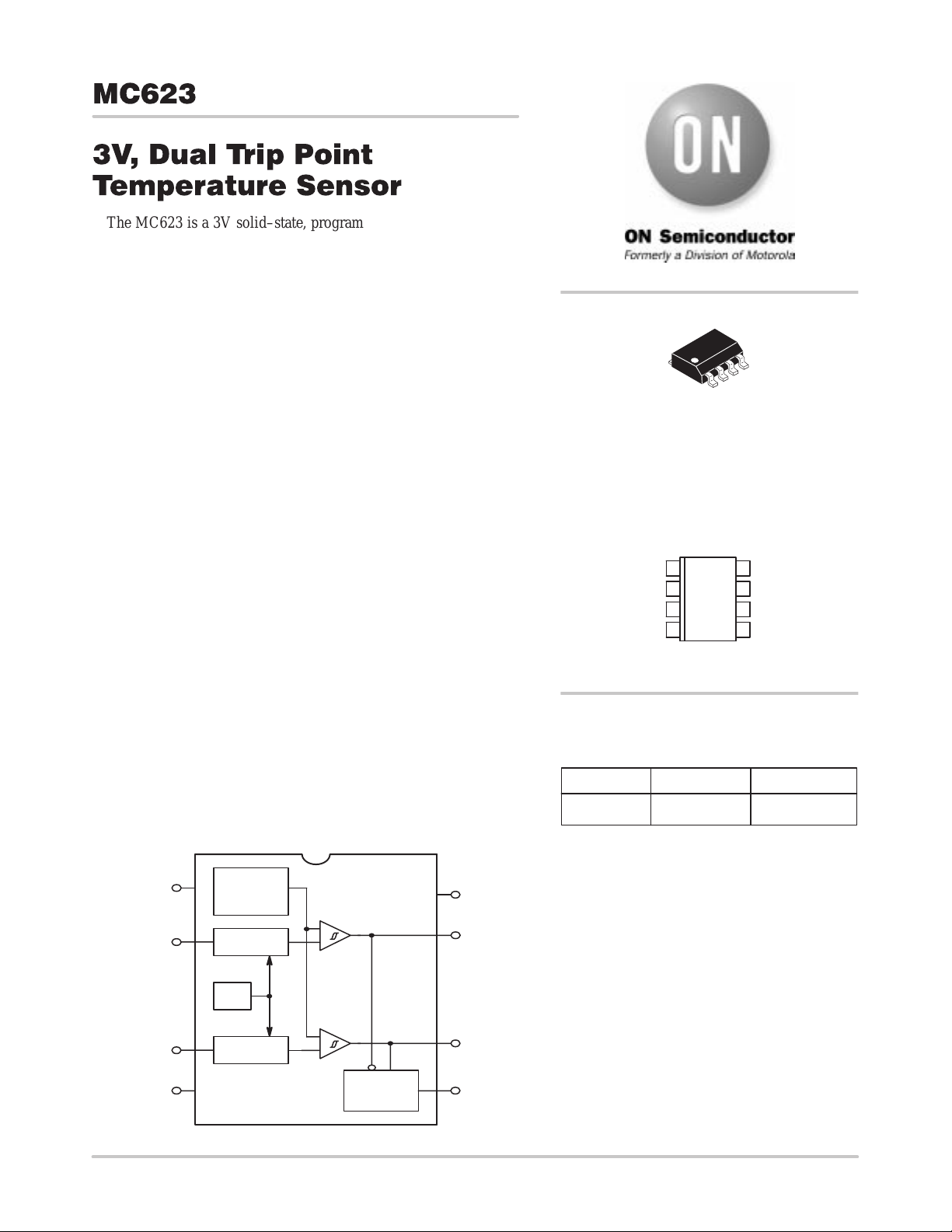
http://onsemi.com
SO–8
D SUFFIX
PRELIMINARY INFORMATION
LOW SET
HIGH SET
ORDERING INFORMATION
Device Package Shipping
MC623DR2 8–Pin SOIC 2500 Tape/Reel
CASE TBD
PIN CONFIGURATION
(Top View)
V
NC
GND
1
2
MC623D
3
4
8
7
LOW LIMIT
6
HIGH LIMIT
5
CONTROL
CC
FUNCTIONAL BLOCK DIAGRAM
1
2
3
4
Temp to
Voltage
Converter
V
ref
V
ref
V
ref
R
LOW
Gen.
Gen.
< R
HIGH
NC
LOW
SET
HIGH
SET
GND
Semiconductor Components Industries, LLC, 1999
February , 2000 – Rev. 0
+
–
+
–
MC623
RS
Latch
V
CC
8
LOW
7
LIMIT
HIGH
6
LIMIT
Q
CONTROL
5
1 Publication Order Number:
MC623/D
Page 2
MC623
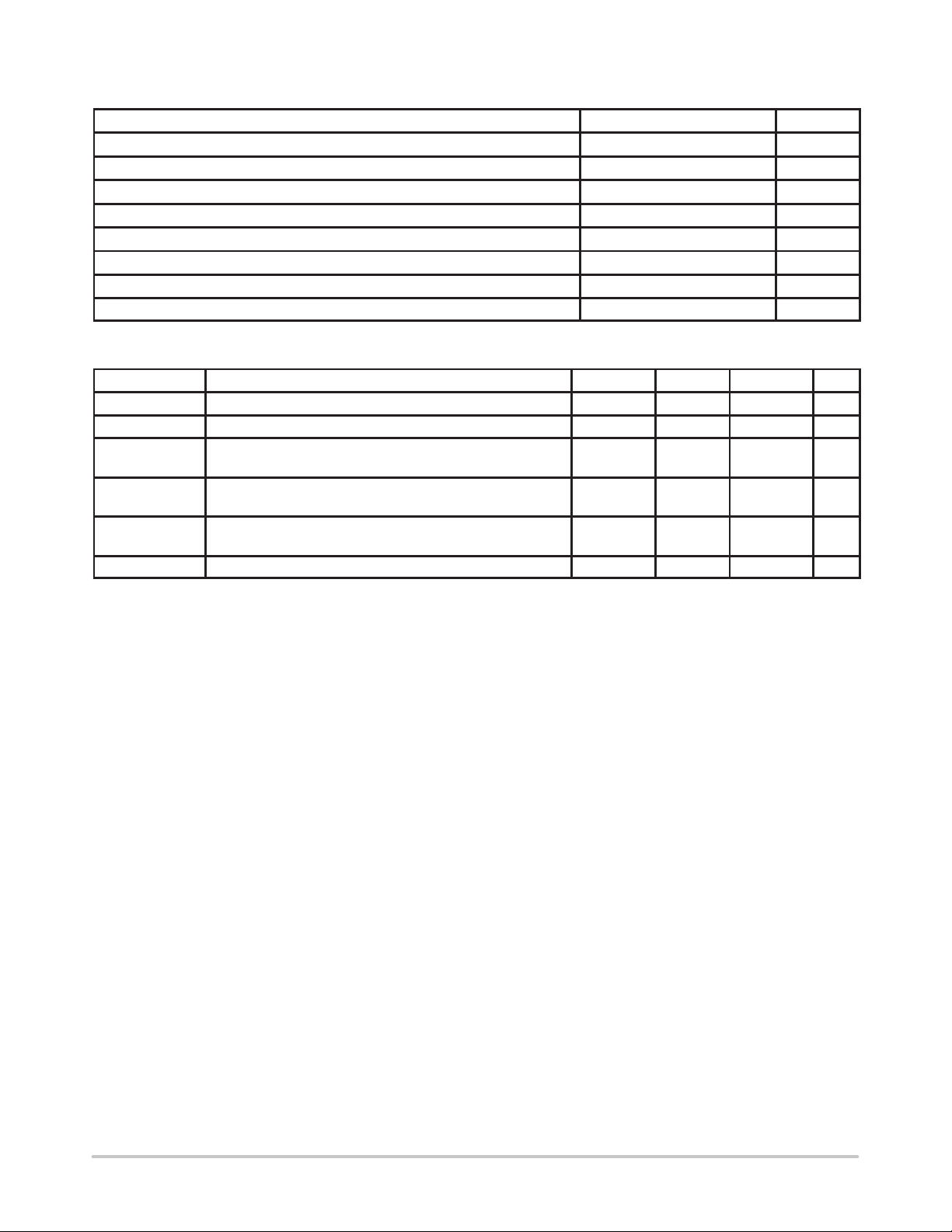
ABSOLUTE MAXIMUM RATINGS*
Parameter Value Unit
Package Power Dissipation (TA ≤ 70°C) 470 mW
Derating Factors 6.0 mW/°C
Supply Voltage 5.5 V
Input Voltage, Any Input (GND – 0.3) to (VDD + 0.3) V
Operating Temperature Range –40 to +125 °C
Maximum Chip Temperature 150 °C
Storage Temperature Range –65 to +150 °C
Lead Temperature (Soldering, 10 Seconds) +300 °C
* Maximum Ratings are those values beyond which damage to the device may occur.
ELECTRICAL CHARACTERISTICS (Over Operating Temperature Range, VDD = 2.7V to 4.5V, unless otherwise noted.)
Symbol Characteristic Min Typ
V
DD
I
DD
V
OH
V
OL
HYST Hysteresis (Falling Temperature) — — –2.0 °C
1. Measured at 25°C.
Supply Voltage Range 2.7 — 4.5 V
Supply Current (2.7V ≤ VDD ≤ 4.5V) — 150 250 µA
Absolute Accuracy
T = Programmed Temperature
IOH = 250µA
IOH = 500µA
IOL = 500µA
IOL = 1.0mA
T–3 T±1 T+3
0.9 x V
DD
0.8 x V
DD
—
—
1
—
—
—
—
Max Unit
—
—
0.1 x V
DD
0.2 x V
DD
°C
V
V
http://onsemi.com
2
Page 3

MC623
DET AILED DESCRIPTION
MC623 Operation
The MC623 consists of a positive temperature coefficient
(PTC) temperature sensor and dual threshold detector.
T emperature set point programming is easily accomplished
with external programming resistors from the HIGH SET
and LOW SET inputs to V
. The HIGH LIMIT and LOW
CC
LIMIT outputs remain inactive (low) as long as the
measured temperature is below setpoint values. As
temperature increases, the LOW LIMIT is driven high when
temperature exceeds the LOW LIMIT setpoint (±3°C). If
temperature continues to climb, the HIGH LIMIT output is
driven high when temperature exceeds the HIGH LIMIT
setpoint (±3°C). Figure 1 shows the relationship between the
sense resistance values and trip point temperature.
250
200
W
150
RESISTANCE (k )
100
To prevent output ”chattering” when measured
temperature is at (or near) the programmed trip point values,
the LOW SET and HIGH SET inputs each have a built–in
hysteresis of - 2°C max. As a result, the HIGH LIMIT and
LOW LIMIT outputs remain active until the measured
temperature falls a maximum of 2°C below the programmed
HIGH SET and LOW SET thresholds as shown in Figure 3.
The programmed setting threshold of Figure 3 is
user–programmed temperature trip points of either the
LOW SET or HIGH SET inputs. The LOW LIMIT or HIGH
LIMIT output is driven active when temperature equals the
programmed setpoint value (to within 3°C). The output
remains active until the temperature falls an additional 2°C
below the setpoint due to hysteresis.
Programmed
Setpoint
–2°C Hysteresis
High Limit or
Low Limit Output
50
5 105
TEMPERATURE (°C)
Figure 1. MC623 Sense Resistors vs. Trip
T emperature
12585654525–15–35–55
The CONTROL output is driven high when the HIGH
LIMIT output goes high, and is reset low when the LOW
LIMIT output goes low. This output provides the logic for
simple ON/OFF fan control. Figure 2 shows overall MC623
operation.
High Set Point
Low Set Point
Low Limit Output
High Limit Output
Control Output
(Cool Option)
Figure 2. MC623 T emperature vs. Output
Temperature
Figure 3. High Set and Low Set Thresholds
APPLICATIONS
Mounting
If the MC623 is used to measure the temperature of
another device, it is important that the top surface of the
MC623 package be in intimate contact with the measured
device. Good thermal conductivity and no air space is
critical to accurate temperature measurement in applications
of this type.
Trip Point Programming
The resistance values required for the HIGH SET and
LOW SET inputs are calculated using the formula below:
R
= 0.5997 x T
TRIP
2.1312
Where Rtrip = Programming resistor value in Ohms
T = Desired trip temperature in degrees Kelvin.
For example, to program a trip point of 50°C, the
programming resistor is:
R
= 0.5997 x (50 + 273.15)
TRIP
2.1312
) = 133,652
W
http://onsemi.com
3
Page 4

MC623
P ACKAGE DIMENSIONS
8–Pin SOIC
PLASTIC PACKAGE
CASE TBD
ISSUE TBD
PIN 1 indicated by dot and/or beveled edge
.157 (3.99)
.150 (3.81)
.244 (6.20)
.228 (5.79)
.050 (1.27) TYP.
.197 (5.00)
.189 (4.80)
.018 (0.46)
.014 (0.36)
.010 (0.25)
.004 (0.10)
.069 (1.75)
.053 (1.35)
_
8 MAX.
.050 (1.27)
.016 (0.40)
.010 (0.25)
.007 (0.18)
Dimensions: inches (mm)
ON Semiconductor and are trademarks of Semiconductor Components Industries, LLC (SCILLC). SCILLC reserves the right to make changes
without further notice to any products herein. SCILLC makes no warranty , representation or guarantee regarding the suitability of its products for any particular
purpose, nor does SCILLC assume any liability arising out of the application or use of any product or circuit, and specifically disclaims any and all liability ,
including without limitation special, consequential or incidental damages. “Typical” parameters which may be provided in SCILLC data sheets and/or
specifications can and do vary in different applications and actual performance may vary over time. All operating parameters, including “Typicals” must be
validated for each customer application by customer’s technical experts. SCILLC does not convey any license under its patent rights nor the rights of others.
SCILLC products are not designed, intended, or authorized for use as components in systems intended for surgical implant into the body, or other applications
intended to support or sustain life, or for any other application in which the failure of the SCILLC product could create a situation where personal injury or
death may occur. Should Buyer purchase or use SCILLC products for any such unintended or unauthorized application, Buyer shall indemnify and hold
SCILLC and its officers, employees, subsidiaries, affiliates, and distributors harmless against all claims, costs, damages, and expenses, and reasonable
attorney fees arising out of, directly or indirectly , any claim of personal injury or death associated with such unintended or unauthorized use, even if such claim
alleges that SCILLC was negligent regarding the design or manufacture of the part. SCILLC is an Equal Opportunity/Affirmative Action Employer .
PUBLICATION ORDERING INFORMATION
NORTH AMERICA Literature Fulfillment:
Literature Distribution Center for ON Semiconductor
P.O. Box 5163, Denver, Colorado 80217 USA
Phone: 303–675–2175 or 800–344–3860 Toll Free USA/Canada
Fax: 303–675–2176 or 800–344–3867 Toll Free USA/Canada
Email: ONlit@hibbertco.com
Fax Response Line: 303–675–2167 or 800–344–3810 T oll Free USA/Canada
N. American Technical Support: 800–282–9855 Toll Free USA/Canada
EUROPE: LDC for ON Semiconductor – European Support
German Phone: (+1) 303–308–7140 (M–F 1:00pm to 5:00pm Munich Time)
Email: ONlit–german@hibbertco.com
French Phone: (+1) 303–308–7141 (M–F 1:00pm to 5:00pm Toulouse T ime)
Email: ONlit–french@hibbertco.com
English Phone: (+1) 303–308–7142 (M–F 12:00pm to 5:00pm UK Time)
Email: ONlit@hibbertco.com
EUROPEAN TOLL–FREE ACCESS*: 00–800–4422–3781
*Available from Germany, France, Italy, England, Ireland
http://onsemi.com
CENTRAL/SOUTH AMERICA:
Spanish Phone: 303–308–7143 (Mon–Fri 8:00am to 5:00pm MST)
Email: ONlit–spanish@hibbertco.com
ASIA/PACIFIC : LDC for ON Semiconductor – Asia Support
Phone: 303–675–2121 (Tue–Fri 9:00am to 1:00pm, Hong Kong Time)
T oll Free from Hong Kong & Singapore:
001–800–4422–3781
Email: ONlit–asia@hibbertco.com
JAPAN: ON Semiconductor, Japan Customer Focus Center
4–32–1 Nishi–Gotanda, Shinagawa–ku, T okyo, Japan 141–8549
Phone: 81–3–5740–2745
Email: r14525@onsemi.com
ON Semiconductor Website: http://onsemi.com
For additional information, please contact your local
Sales Representative.
MC623/D
4
 Loading...