

Page 1
4-220
FAST AND LS TTL DATA
4-BIT BIDIRECTIONAL COUNTERS
(WITH 3-STATE OUTPUTS)
The MC54/ 74F568 and MC54/74F569 are fully synchronous, reversible
counters with 3-state outputs. The F568 is a BCD decade counter; the F569
is a binary counter. They feature preset capability for programmable operation, carry lookahead for easy cascading, and a U/D
input to control the direction of counting. For maximum flexibility there are both synchronous and master asynchronous reset inputs as well as both Clocked Carry (CC
) and
Terminal Count (TC
) outputs. All state changes except Master Reset are initi-
ated by the rising edge of the clock. A HIGH signal on the Output Enable (OE
)
input forces the output buffers into the high impedance state but does not prevent counting, resetting or parallel loading.
• 4-Bit Bidirectional Counting
F568 Decade Counter
F569 Binary Counter
• Synchronous Counting and Loading
• Lookahead Carry Capability for Easy Cascading
• Preset Capability for Programmable Operation
• 3-State Outputs for Bus Organized Systems
• Master Reset (MR) Overrides All Other Inputs
• Synchronous Reset (SR) Overrides Counting and Parallel Loading
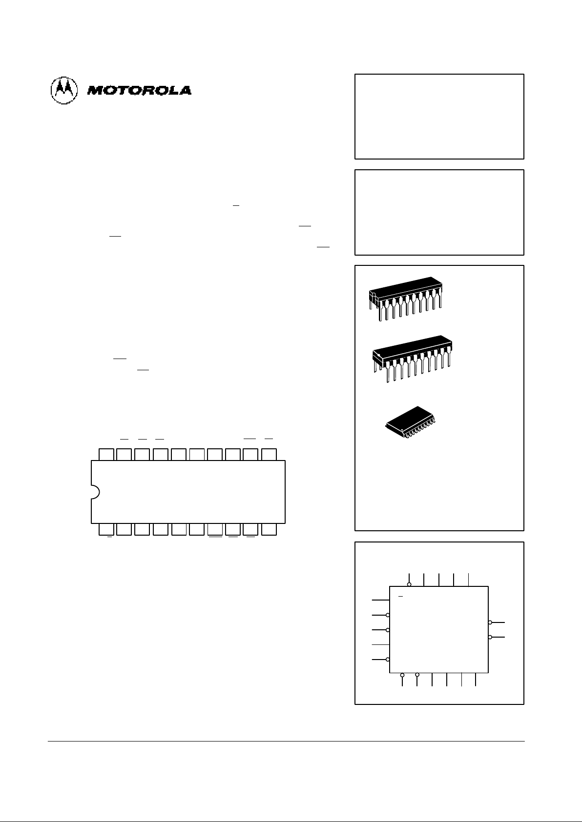
CONNECTION DIAGRAM
18 17 16 15 14 13
1 2 3 4 5 6
7
20 19
8
V
CC
U/D
TC CC OE O
0
O
2
O
1
O
3
CP P0P1P2P3CEP
MR
9 10
SR
GND
12 11
CET
PE
MC54/74F568
MC54/74F569
4-BIT
BIDIRECTIONAL
COUNTERS
(WITH 3-STATE OUTPUTS)
FAST SCHOTTKY TTL
ORDERING INFORMATION
MC54FXXXJ Ceramic
MC74FXXXN Plastic
MC74FXXXDW SOIC
20
1
J SUFFIX
CERAMIC
CASE 732-03
20
1
N SUFFIX
PLASTIC
CASE 738-03
20
1
DW SUFFIX
SOIC
CASE 751D-03
LOGIC SYMBOL
PE P0P1P2P
3
U/D
CEP
CET
CP
OE
MR SR O0O1O2O
3
CC
TC
11 3 54 6
18
19
8 9 16 15 14 13
1
7
12
2
17
Page 2
4-221
FAST AND LS TTL DATA
MC54/74F568 • MC54/74F569
Symbol Parameter Min Typ Max Unit
V
CC
Supply Voltage 54, 74 4.5 5.0 5.5 V
54 –55 25 125
TAOperating Ambient Temperature Range
74 0 25 70
°C
I
OH
Output Current — High 54, 74 –3.0 mA
I
OL
Output Current — Low 54, 74 24 mA
FUNCTIONAL DESCRIPTION
The F568 counts modulo-10 in the BCD (8421) sequence.
From state 9 (HLLH) it will increment to 0 (LLLL) in the Up
mode; in Down mode it will decrement from 0 to 9.The F569
counts in the modulo-16 binary sequence. From state 15 it will
increment to state 0 in the Up mode; in the Down mode it will
decrement from 0 to 15. The clock inputs of all flip-flops are
driven in parallel through a clock buffer. All state changes (except due to Master Reset) occur synchronously with the LOWto-HIGH transition of the Clock Pulse (CP) input signal.
The circuits have five fundamental modes of operation, in
order of precedence: asynchronous reset, synchronous reset,
parallel load, count and hold. Five control inputs — Master Reset (MR
), Synchronous Reset (SR), Parallel Enable (PE),
Count Enable Parallel (CEP
) and Count Enable Trickle (CET)
— plus the Up/Down (U/D
) input, determine the mode of operation, as shown in the Mode Select Table. A LOW signal on
MR
overrides all other inputs and asynchronously forces the
flip-flop Q outputs LOW. A LOW signal on SR
overrides counting and parallel loading and allows the Q outputs to go LOW
on the next rising edge of CP. A LOW signal on PE
overrides
counting and allows information on the Parallel Data (Pn) inputs to be loaded into the flip-flops on the next rising edge of
CP. With MR
, SR and PE HIGH, CEP and CET permit counting
when both are LOW. Conversely , a HIGH signal on either CEP
or CET inhibits counting.
The F568 and F569 use edge-triggered flip-flops and
changing the SR
, PE, CEP , CET or U/D inputs when the CP
is in either state does not cause errors, provided that the recommended setup and hold times, with respect to the rising
edge of CP, are observed.
Two types of outputs are provided as overflow/underflow in-
dicators. The Terminal Count (TC
) output is normally HIGH
and goes LOW providing CET
is LOW, when the counter
reaches zero in the Down mode, or reaches maximum (9 for
the F568,15 for the F569) in the Up mode. TC
will then remain
LOW until a state change occurs, whether by counting or presetting, or until U/D
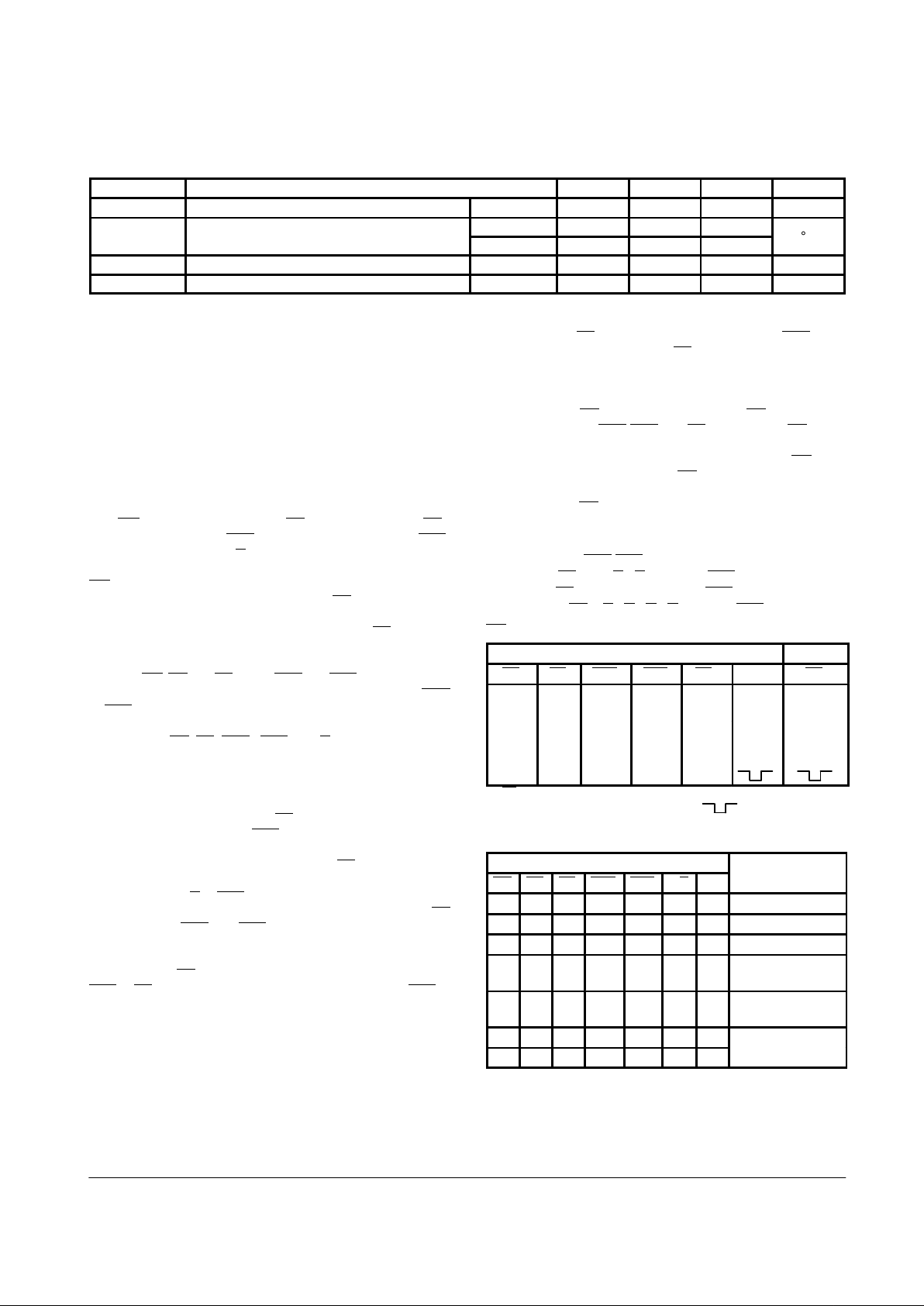
or CET is changed. T o implement synchronous multistage counters, the connections between the TC
output and the CEP and CET inputs can provide either slow
or fast carry propagation. Figure A shows the connections for
simple ripple carry, in which the clock period must be longer
than the CP to TC
delay of the first stage, plus the cumulative
CET
to TC delays of the intermediate stages, plus the CET to
CP setup time of the last stage. This total delay plus setup time
sets the upper limit on clock frequency. For faster clock rates,
the carry lookahead connections shown in Figure B are recommended. In this scheme the ripple delay through the intermediate stages commences with the same clock that causes
the first stage to tick over from max to min in the Up mode, or
min to max in the Down mode, to start its final cycle. Since this
final cycle takes 10 (F568) or 16 (F569) clocks to complete,
there is plenty of time for the ripple to progress through the intermediate stages. The critical timing that limits the clock peri-
od is the CP to TC
delay of the first stage plus the CEP to CP
setup time of the last stage. The TC
output is subject to decoding spikes due to internal race conditions and is therefore not
recommended for use as a clock or asynchronous reset for
flip-flops, registers or counters. For such applications, the
Clocked Carry (CC
) output is provided. The CC output is nor-
mally HIGH. When CEP
, CET , and TC are LOW, the CC output
will go LOW when the clock next goes LOW and will stay LOW
until the clock goes HIGH again, as shown in the CC
Truth
Table. When the Output Enable (OE
) is LOW, the parallel data
outputs O0–O3 are active and follow the flip-flop Q outputs. A
HIGH signal on OE
forces O0–O3 to the High Z state but does
not prevent counting, loading or resetting.
LOGIC EQUATIONS:
Count Enable = CEP
⋅CET⋅PE
Up (’F568): TC
= Q0⋅Q
1⋅Q2⋅Q3
⋅(Up)⋅CET
(’F569): TC = Q0⋅Q1⋅Q2⋅Q3⋅(Up)⋅CET
Down (Both): TC = Q
0⋅Q1⋅Q2⋅Q3
⋅(Down)⋅CET
CC TRUTH TABLE
Inputs Output
SR PE CEP CET TC* CP CC
L X X X X X H
X L X X X X H
X X H X X X H
X X X H X X H
X X X X H X H
H H L L L
* = TC is generated internally X = Don’t Care
L = LOW Voltage Level
= Low Pulse
H = HIGH Voltage Level
FUNCTION TABLE
Inputs
MR SR PE CEP CET U/D CP
Operating Mode
L X X X X X X Asynchronous reset
h l X X X X ↑ Synchronous reset
h h l X X X ↑ Parallel load
h h h l l h ↑
Count up
(increment)
h h h l l l ↑
Count down
(decrement)
h H H H X X X
h H H X H X X
Hold (do nothing)
H = HIGH voltage level
h = HIGH voltage level one setup prior to the Low-to-High Clock transition
L = LOW voltage level
l = LOW voltage level one setup prior to the Low-to-High clock transition
X = Don’t care
↑ = Low-to-High clock transition
Page 3

C
D
P
PE
U/D
CP
MR
OE
TC
DETAIL A
LD T BT
BF
ENF
SR
CP
LDT
AT
AF
UPDNSR
J CP K
QQ
DETAIL A
0
P
1
P
2
P
3
O
0
C
D
CEP
CET
SR
CP
Q C
D
UP
DN
Q
DETAIL A
CP
CC
O
1
O
2
O
3
P
0
P
1
P
2
P
3
PE
U/D
CP
MR
OE
CEP
CET
SR
LDT
UPDNSR
AT
AF
C
D
LD T BT
BF
ENF
SR
CPUPDN
Q
DETAIL A
DETAIL A
CP
TC
CC
O
0
O
1
O
2
O
3
DETAIL A Q
C
D
CP
J CP K
QQ
C
D
MC54/74F569MC54/74F568
DETAIL A
DETAIL A
ENF
ENF
LOGIC DIAGRAMS
Please note that these diagrams are provided only for the understanding of logic
operations and should not be used to estimate propagation delays.
4-222
FAST AND LS TTL DATA
MC54/74F568 • MC54/74F569
Page 4

4-223
FAST AND LS TTL DATA
MC54/74F568 • MC54/74F569
Figure A. Multistage Counter with Ripple Carry
Figure B. Multistage Counter with Lookahead Carry
COUNT CETCPTC CET TC CET TC CET TC CET
CP TO ALL STAGES
COUNT
CP
CETCPTC CEP
CET TC
CEP
CET TC
CEP
CET TC
CEP
CET
TO ALL STAGES
L
DC CHARACTERISTICS OVER OPERATING TEMPERATURE RANGE (unless otherwise specified)
Limits
Symbol
Parameter
Min Typ Max
Unit
Test Conditions
V
IH
Input HIGH Voltage 2.0 V
Guaranteed Input HIGH Voltage for
All Inputs
V
IL
Input LOW Voltage 0.8 V
Guaranteed Input LOW Voltage for
All Inputs
V
IK
Input Clamp Diode Voltage –1.2 V VCC = MIN, IIN = –18 mA
54, 74 2.4 3.3 V IOH = –3.0 mA VCC = 4.5 V
VOHOutput HIGH Voltage
74 2.7 3.3 V IOH = –3.0 mA VCC = 4.75 V
V
OL
Output LOW Voltage 0.3 0.5 V IOL = 24 mA VCC = MIN
I
OZH
Output OFF Current — HIGH 50 µA V
OUT
= 2.7 V VCC = MAX
I
OZL
Output OFF Current — LOW –50 µA V
OUT
= 0.5 V VCC = MAX
20
VIN = 2.7 V
IIHInput HIGH Current
100
µA
VIN = 7.0 V
VCC = MAX
I
IL
Input LOW Current
PE
, CET
Others
–1.2
–0.6
mA VCC = MAX, VIN = 0.5 V
I
OS
Output Short Circuit Current (Note 2) –60 –150 mA V
OUT
= 0 V VCC = MAX
I
CC
Power Supply Current
(ALL Outputs OFF)
67 mA VCC = MAX
NOTES:
1. For conditions such as MIN or MAX, use the appropriate value specified under recommended operating conditions for the applicable device type.
2. Not more than one output should be shorted at a time, nor for more than 1 second.
Page 5

4-224
FAST AND LS TTL DATA
MC54/74F568 • MC54/74F569
13
4
MC54/74F568
MC54/74F569
STATE DIAGRAMS
COUNT DOWN
COUNT UP
COUNT DOWN
COUNT UP
0 1 2 3
12567
8
9
0 1 2 3
4
5
6
7
891011
12
13
14
15
11
10
14
15
AC CHARACTERISTICS
54/74F 54F 74F
TA= +25°C
VCC= +5.0 V
CL= 50pF
TA= –55 to +125°C
VCC= 5.0V ±10%
CL= 50pF
TA= 0 to +70°C
VCC= 5.0V ±10%
CL= 50pF
Symbol
Parameter
Min Max Min Max Min Max
Unit
f
max
Maximum Clock Frequency 100 60 85 MHz
t
PLH
t
PHL
Propagation Delay
CP to On (PE
HIGH or LOW)
3.0
4.0
8.5
11.5
3.0
4.0
10.5
14
3.0
4.0
9.5
13
ns
t
PLH
t
PHL
Propagation Delay
CP to TC
5.5
4.0
15.5
11
5.5
4.0
18.5
13.5
5.5
4.0
17.5
12.5
ns
t
PLH
t
PHL
Propagation Delay
CET
to TC
2.5
2.5
6.0
8.0
2.5
2.5
8.0
10
2.5
2.5
7.0
9.0
ns
t
PLH
t
PHL
Propagation Delay
U/D
to TC (′F568)
3.5
4.0
11
16
3.5
4.0
13.5
19
3.5
4.0
12.5
18
ns
t
PLH
t
PHL
Propagation Delay
U/D
to TC (′F569)
3.5
4.0
11
10.5
3.5
4.0
13.5
13
3.5
4.0
12.5
12
ns
t
PLH
t
PHL
Propagation Delay
CP to CC
2.5
2.0
7.0
6.0
2.5
2.0
9.0
8.0
2.5
2.0
8.0
7.0
ns
t
PLH
t
PHL
Propagation Delay
CEP
, CET to CC
2.5
4.0
6.5
11
2.5
4.0
8.5
13.5
2.5
4.0
7.5
12.5
ns
t
PHL
Propagation Delay
MR
to O
n
5.0 13 5.0 15.5 5.0 14.5 ns
t
PZH
t
PZL
Output Enable Time
OE
to O
n
2.5
3.0
7.0
8.0
2.5
3.0
9.0
10
2.5
3.0
8.0
9.0
ns
t
PHZ
t
PLZ
Output Disable Time
OE
to O
n
1.5
2.0
6.5
6.0
1.5
2.0
8.5
8.0
1.5
2.0
7.5
7.0
ns
Page 6

4-225
FAST AND LS TTL DATA
MC54/74F568 • MC54/74F569
AC OPERATING REQUIREMENTS
54/74F 54F 74F
TA= +25°C
VCC= +5.0 V
TA= –55°C to +125°C
VCC= 5.0V ±10%
TA= 0°C to +70°C
VCC= 5.0V ±10%
Symbol
Parameter
Min Max Min Max Min Max
Unit
ts(H)
ts(L)
Setup Time, HIGH or LOW
Pn to CP
4.0
4.0
5.5
5.5
4.5
4.5
th(H)
th(L)
Hold Time, HIGH or LOW
Pn to CP
3.0
3.0
3.5
3.5
3.5
3.5
ns
ts(H)
ts(L)
Setup Time, HIGH or LOW
CEP
or CET to CP
5.0
5.0
7.0
7.0
6.0
6.0
th(H)
th(L)
Hold Time, HIGH or LOW
CEP
or CET to CP
0
0
0
0
0
0
ns
ts(H)
ts(L)
Setup Time, HIGH or LOW
PE
to CP
8.0
8.0
10
10
9.0
9.0
th(H)
th(L)
Hold Time, HIGH or LOW
PE
to CP
0
0
0
0
0
0
ns
ts(H)
ts(L)
Setup Time, HIGH or LOW
U/D
to CP (F568)
11
16.5
13.5
18.5
12.5
17.5
ns
ts(H)
ts(L)
Setup Time, HIGH or LOW
U/D
to CP (F569)
11
7.0
13.5
10
12.5
8.0
ns
th(H)
th(L)
Hold Time, HIGH or LOW
U/D
to CP
0
0
0
0
0
0
ns
ts(H)
ts(L)
Setup Time, HIGH or LOW
SR
to CP
10
8.0
12
10.5
11
9.5
th(H)
th(L)
Hold Time, HIGH or LOW
SR
to CP
0
0
0
0
0
0
ns
tw(H)
tw(L)
CP Pulse Width HIGH or LOW
4.0
6.0
6.0
8.0
4.5
6.5
ns
tw(L) MR Pulse Width, LOW 4.5 6.0 5.0 ns
t
rec
MR Recovery Time 6.0 8.0 7.0 ns
 Loading...