

Page 1
4-130
FAST AND LS TTL DATA
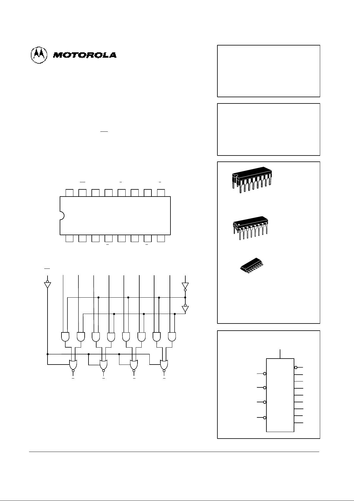
QUAD 2-INPUT MULTIPLEXER
WITH 3-STATE OUTPUTS
The MC74F258A is a quad 2-input multiplexer with 3-state outputs. Four
bits of data from two sources can be selected using a common Data Select
input. The four outputs present the selected data in the complement (inverted)
form. The outputs may be switched to a high impedance state with a HIGH
on the common Output Enable (OE) input, allowing the outputs to interface directly with bus-oriented systems.
• Multiplexer Expansion by Tying Outputs Together
• Inverting 3-State Outputs
• AC Enhanced Version of the F258
CONNECTION DIAGRAM (TOP VIEW)
1516 14 13 12 11 10
21 3 4 5 6 7
V
CC
9
8
OE
I0cI
1c
Z
cI0dI1dZd
S I
0aI1aZaI0bI1bZb
GND
LOGIC DIAGRAM
I
0aI1aI0bI1bI0C
I
1b
I
1CI0DSI1C
Z
a
Z
b
Z
d
Z
c
OE
FAST SCHOTTKY TTL
QUAD 2-INPUT MULTIPLEXER
WITH 3-STATE OUTPUTS
MC74F258A
J SUFFIX
CERAMIC
CASE 620-09
N SUFFIX
PLASTIC
CASE 648-08
16
1
16
1
ORDERING INFORMATION
MC54FXXXAJ Ceramic
MC74FXXXAN Plastic
MC74FXXXAD SOIC
16
1
D SUFFIX
SOIC
CASE 751B-03
LOGIC SYMBOL
12
13
14
15
2
3
4
7
5
6
11
10
9
Z
a
Z
b
Zc
Z
d
I
1a
I
0a
OE
I
0c
I
1c
I
1d
I
0d
I
0b
I
1b
1
S
VCC = PIN 16
GND = PIN 8
Page 2
4-131
FAST AND LS TTL DATA
MC74F258A
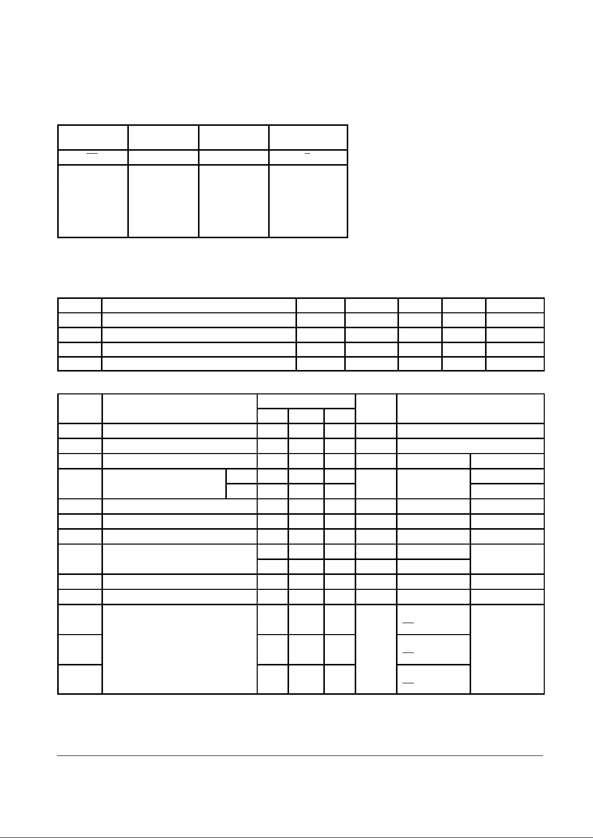
FUNCTION TABLE
Output
Enable
Select
Input
Data
Inputs
Output
OE S I
0
I
1
Z
H X X X Z
L H X L H
L H X H L
L L L X H
L L H X L
H = HIGH Voltage Level
L = LOW Voltage Level
X = Don’t Care
Z = High Impedance
GUARANTEED OPERATING RANGES
Symbol Parameter Min Typ Max Unit
V
CC
Supply Voltage 74 4.5 5.0 5.5 V
T
A
Operating Ambient Temperature Range 74 0 25 70 °C
I
OH
Output Current — High 74 –3.0 mA
I
OL
Output Current — Low 74 24 mA
DC CHARACTERISTICS OVER OPERATING TEMPERATURE RANGE (unless otherwise specified)
Limits
Symbol Parameter Min Typ Max Unit Test Conditions
V
IH
Input HIGH Voltage 2.0 V Guaranteed Input HIGH Voltage
V
IL
Input LOW Voltage 0.8 V Guaranteed Input LOW Voltage
V
IK
Input Clamp Diode Voltage –1.2 V IIN = –18 mA VCC = MIN
V
OH
Output HIGH Voltage 74 2.7 3.3 V IOH = –3.0 mA VCC = 4.75 V
74 2.4 VCC = MIN
V
OL
Output LOW Voltage 0.35 0.5 V IOL = 24 mA VCC = MIN
I
OZH
Output OFF Current — HIGH 50 µA V
OUT
= 2.7 V VCC = MAX
I
OZL
Output OFF Current — LOW –50 µA V
OUT
= 0.5 V VCC = MAX
I
IH
Input HIGH Current 20 µA VIN = 2.7 V VCC = MAX
100 µA VIN = 7.0 V
I
IL
Input LOW Current –0.6 mA VIN = 0.5 V VCC = MAX
I
OS
Output Short Circuit Current (Note 2) –60 –150 mA V
OUT
= 0 V VCC = MAX
I
CCH
6.2 9.5 S, I1x = 4.5 V
OE, I0x = GND
I
CCL
Power Supply Current 15.1 23 mA I1x = 4.5 V VCC = MAX
OE, I0x, S = GND
I
CCZ
11.3 17 S, I0x = GND
OE, I1x = 4.5 V
NOTES:
1. For conditions shown as MIN or MAX, use the appropriate value specified under guaranteed operating ranges.
2. Not more than one output should be shorted at a time, nor for more than 1 second.
Page 3

4-132
FAST AND LS TTL DATA
MC74F258A
AC CHARACTERISTICS
74F 74F
TA = +25°C TA = 0°C to 70°C
VCC = +5.0 V VCC = 5.0 V ± 10%
CL = 50 pF CL = 50 pF
Symbol Parameter Min Max Min Max Unit
t
PLH
Propagation Delay 2.5 5.3 2.0 6.0 ns
t
PHL
In to Z
n
1.0 4.0 1.0 5.0
t
PLH
Propagation Delay 3.0 7.5 3.0 8.5 ns
t
PHL
S to Z
n
2.5 7.0 2.5 8.0
t
PZH
Output Enable Time 2.0 6.0 2.0 7.0 ns
t
PZL
2.5 7.0 2.5 8.0
t
PHZ
Output Disable Time 2.0 6.0 2.0 7.0 ns
t
PLZ
1.5 6.0 1.5 7.0
FUNCTIONAL DESCRIPTION
The F258A is a quad 2-input multiplexer with 3-state outputs. It selects four bits of data from two sources under control
of a common Select input (S). When the Select input is LOW,
the I0x inputs are selected and when Select is HIGH, the I1x
inputs are selected. The data on the selected inputs appears
at the outputs in inverted form. The F258A is the logic implementation of a 4-pole, 2-position switch where the position of
the switch is determined by the logic levels supplied to the Select input. The logic equations for the outputs are shown below:
Z
a
= OE
• (I1a • S + I0a • S)
Z
b
= OE
• (I1b • S + I0b • S)
Z
c
= OE
• (I1c • S + I0c • S)
Z
d
= OE
• (I1d • S + I0d • S)
When the Output Enable input (OE
) is HIGH, the outputs are
forced to a high impedance OFF state. If the outputs of the
3-state devices are tied together, all but one device must be in
the high impedance state to avoid high currents that would exceed the maximum ratings. Designers should ensure the Output Enable signals to 3-state devices whose outputs are tied
together are designed so there is no overlap.
 Loading...