

Page 1
4-89
FAST AND LS TTL DATA
QUAD D FLIP-FLOP
The MC54/74F175 is a high-speed quad D flip-flop. The device is useful for
general flip-flop requirements where both true and complementary outputs
are required and clock and clear inputs are common to all flip-flops. The information on the D inputs is stored during the LOW-to-HIGH clock transition.
Both true and complemented outputs of each flip-flop are provided. A Master
Reset input resets all flip-flops, independent of the Clock or D inputs when
LOW.
• Four Edge-triggered D-type Inputs
• Buffered Positive Edge-triggered Common Clock
• Buffered Asynchronous Common Reset
• True and Complementary Outputs
• ESD
>
4000 Volts
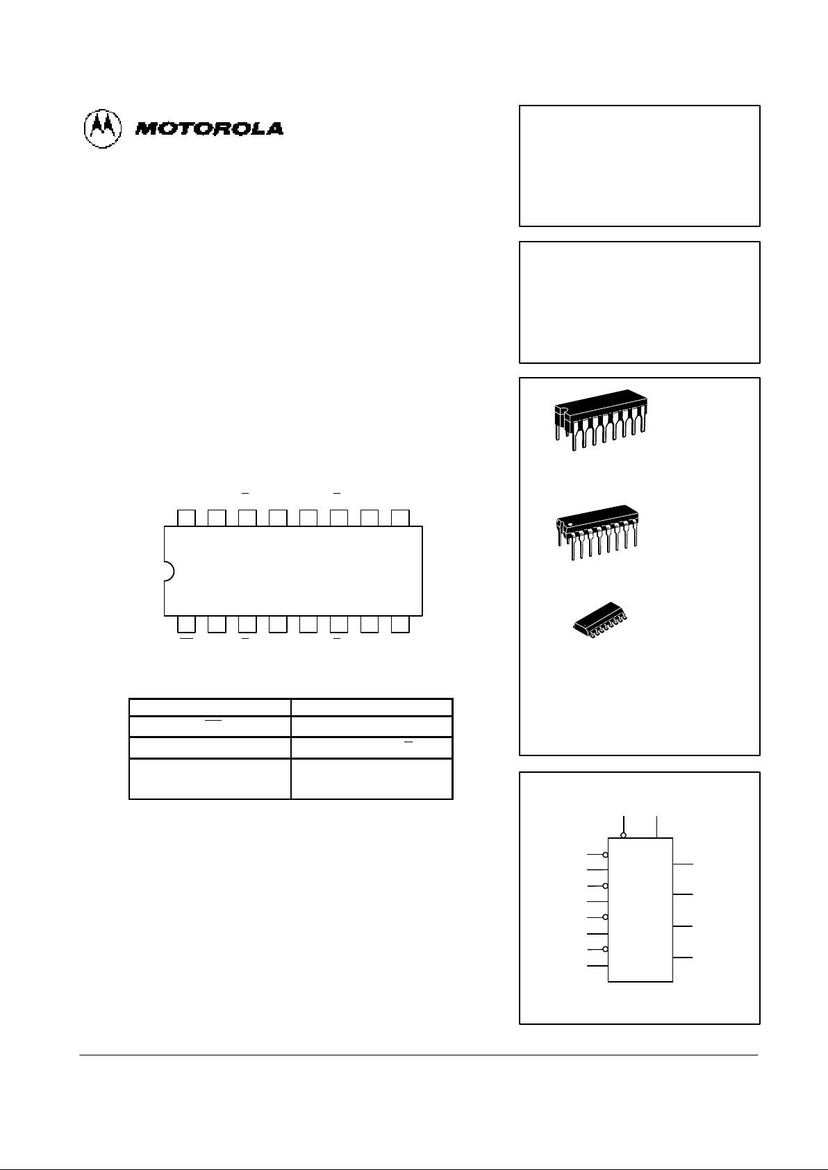
CONNECTION DIAGRAM DIP (TOP VIEW)
1516 14 13 12 11 10
21 3 4 5 6 7
V
CC
9
8
Q3Q
3D3D2Q2Q2
CP
MR
Q0Q
0D0D1Q1Q1
GND
FUNCTION TABLE
Inputs Outputs
@ tn, MR = H @ tn + 1
D
n
Q
n
Q
n
L L H
H H L
tn = Bit time before clock positive-going transition
tn + 1 = Bit time after clock positive-going transition
H = HIGH Voltage Level
L = LOW Voltage Level
MC54FXXXJ Ceramic
MC74FXXXN Plastic
MC74FXXXD SOIC
MC54/74F175
QUAD D FLIP-FLOP
FAST SCHOTTKY TTL
J SUFFIX
CERAMIC
CASE 620-09
N SUFFIX
PLASTIC
CASE 648-08
16
1
16
1
ORDERING INFORMATION
16
1
D SUFFIX
SOIC
CASE 751B-03
LOGIC SYMBOL
1 9
4
5
12
13
3
2
6
7
11
10
14
15
D
2
D
1
D
0
Q
2
Q
1
Q
0
CPMR
D
3
Q
3
Q
3
Q
2
Q
1
Q
0
VCC = PIN 16
GND = PIN 8
Page 2
4-90
FAST AND LS TTL DATA
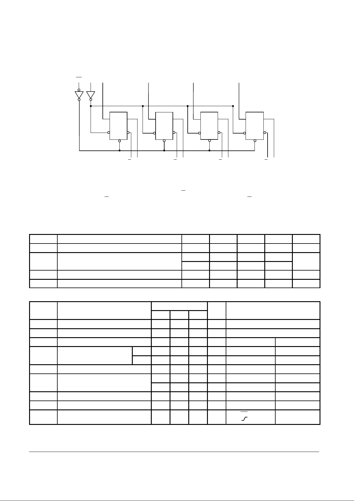
MC54/74F175
D
CP
D
CP
D
CP
LOGIC DIAGRAM
D
3
D
1
D
0
D
2
Q
3
CPMR
Q
CD
Q
CD
Q
CD
D Q
CP
CD
Q
3
Q2Q
2
Q1Q
1
Q0Q
0
Q Q Q Q
NOTE:
This diagram is provided only for the understanding of logic operations and should not be used to estimate propagation delays.
FUNCTIONAL DESCRIPTION
The F175 consists of four edge-triggered D flop-flops with
individual D inputs and Q and Q outputs. The Clock and
Master Reset are common. The four flip-flops will store the
state of their individual D inputs, one setup time before, on the
LOW-to-HIGH clock (CP) transition, causing individual Q and
Q
outputs to follow. A LOW input on the Master Reset (MR) will
force all Q outputs LOW and Q
outputs HIGH independent of
Clock or Data inputs. The F175 is useful for general logic
applications where a common Master Reset and Clock are
acceptable.
GUARANTEED OPERATING RANGES
Symbol Parameter Min Typ Max Unit
V
CC
Supply Voltage 54, 74 4.5 5.0 5.5 V
T
A
Operating Ambient Temperature Range
54 –55 25 125 °C
A
74 0 25 70
I
OH
Output Current — High 54, 74 –1.0 mA
I
OL
Output Current — Low 54, 74 20 mA
DC CHARACTERISTICS OVER OPERATING TEMPERATURE RANGE (unless otherwise specified)
Limits
Symbol Parameter Min Typ Max Unit Test Conditions
V
IH
Input HIGH Voltage 2.0 V Guaranteed Input HIGH Voltage
V
IL
Input LOW Voltage 0.8 V Guaranteed Input LOW Voltage
V
IK
Input Clamp Diode Voltage –1.2 V IIN = –18 mA VCC = MIN
V
OH
Output HIGH Voltage 54, 74 2.5 3.4 V IOH = – 1.0 mA VCC = 4.50 V
74 2.7 3.4 V IOH = – 1.0 mA VCC = 4.75 V
V
OL
Output LOW Voltage 0.35 0.5 V IOL = 20 mA VCC = MIN
I
IH
Input HIGH Current 20 µA VIN = 2.7 V VCC = MAX
100 µA VIN = 7.0 V VCC = MAX
I
IL
Input LOW Current –0.6 mA VIN = 0.5 V VCC = MAX
I
OS
Output Short Circuit Current (Note 2) –60 –150 mA V
OUT
= 0 V VCC = MAX
I
CC
Power Supply Current 22.5 34 mA Dn = MR = 4.5 V
CP =
VCC = MAX
NOTES:
1. For conditions shown as MIN or MAX, use the appropriate value specified under guaranteed operating ranges.
2. Not more than one output should be shorted at a time, nor for more than 1 second.
Page 3

4-91
FAST AND LS TTL DATA
MC54/74F175
AC CHARACTERISTICS
54/74F 54F 74F
TA = +25°C TA = –55°C to +125°C TA = 0°C to +70°C
VCC = +5.0 V VCC = 5.0 V ± 10% VCC = 5.0 V ± 10%
CL = 50 pF CL = 50 pF CL = 50 pF
Symbol Parameter Min Typ Max Min Max Min Max Unit
f
max
Maximum Clock Frequency 100 140 100 100 MHz
t
PLH
Propagation Delay 3.5 5.0 6.5 3.5 8.5 3.5 7.5 ns
t
PHL
CP to Qn or Q
n
4.0 6.5 8.5 4.0 10.5 4.0 9.5
t
PHL
Propagation Delay
MR to Q
n
4.5 9.0 11.5 4.5 15 4.5 13 ns
t
PLH
Propagation Delay
MR to Q
n
4.0 6.5 8.5 4.0 10 4.0 9.0 ns
AC OPERATING REQUIREMENTS
54/74F 54F 74F
TA = +25°C TA = –55°C to +125°C TA = 0°C to +70°C
VCC = +5.0 V VCC = 5.0 V ± 10% VCC = 5.0 V ± 10%
Symbol Parameter Min Typ Max Min Max Min Max Unit
ts(H) Setup Time, HIGH or LOW 3.0 3.0 3.0
ts(L) Dn to CP 3.0 3.0 3.0 ns
th(H) Hold Time, HIGH or LOW 1.0 1.0 1.0
th(L) Dn to CP 1.0 1.0 1.0
tw(H) CP Pulse Width, HIGH 4.0 4.0 4.0 ns
tw(L) or LOW 5.0 5.0 5.0
tw(L) MR Pulse Width, LOW 5.0 5.0 5.0 ns
t
rec
Recovery Time, MR to CP 5.0 5.0 5.0 ns
 Loading...