

Page 1
4-82
FAST AND LS TTL DATA
4-STAGE SYNCHRONOUS
BIDIRECTIONAL COUNTERS
The MC54/74F168 and MC54/74F169 are fully synchronous 4-stage up/
down counters. The F168 is a BCD decade counter; the F169 is a modulo-16
binary counter. Both feature a preset capability for programmable operation,
carry lookahead for easy cascading, and a U/D
input to control the direction
of counting. All state changes, whether in counting or parallel loading, are initiated by the LOW-to-HIGH transition of the clock.
• Asynchronous Counting and Loading
• Built-In Lookahead Carry Capability
• Presettable for Programmable Operation
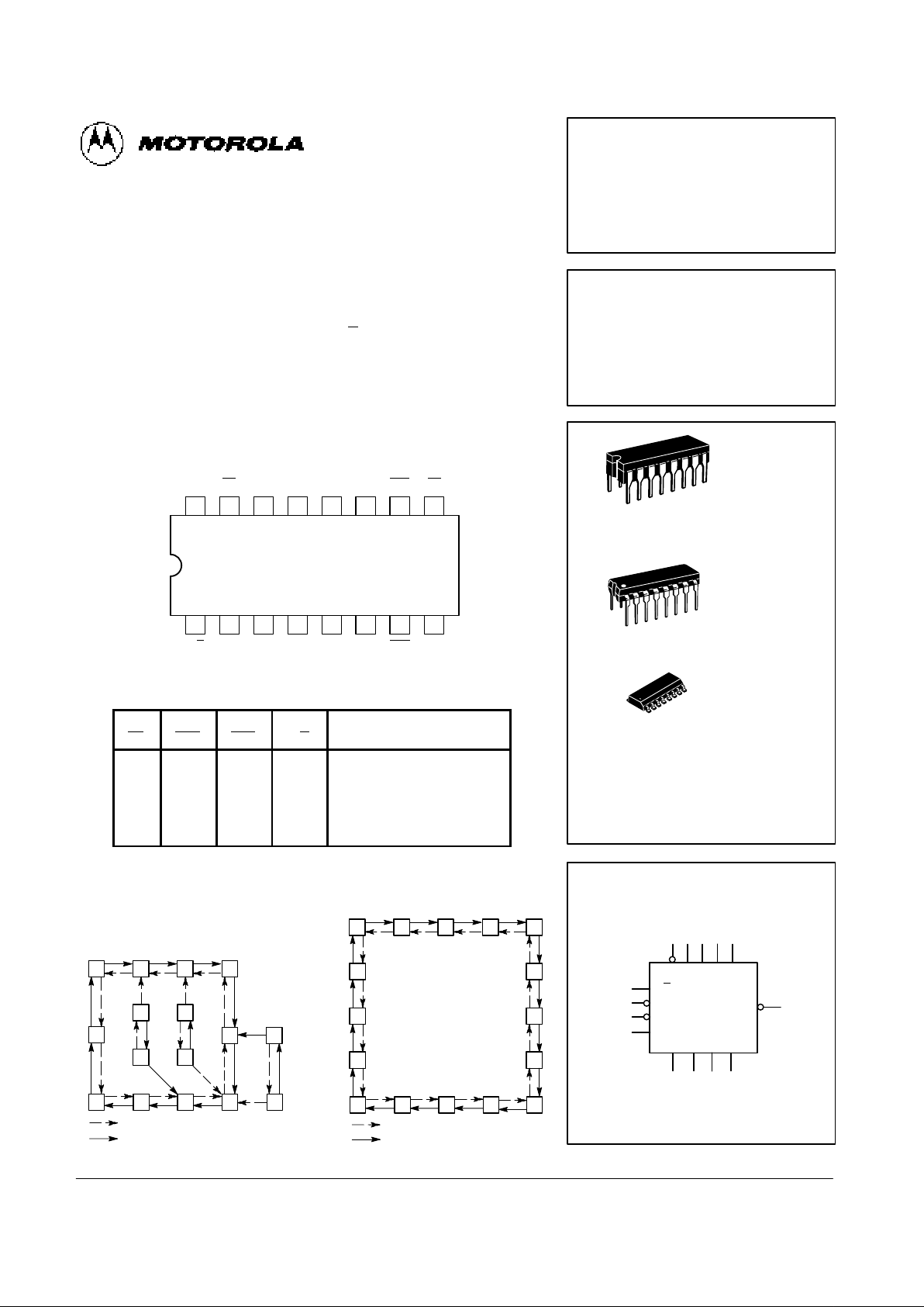
CONNECTION DIAGRAM (TOP VIEW)
1516 14 13 12 11 10
21 3 4 5 6 7
V
CC
9
8
TC
Q0Q1Q2Q3CET PE
U/D CP P0P1P2P3CEP GND
MODE SELECT TABLE
PE CEP CET U/D
Action on Rising
Clock Edge
L X X X
Load (Pn º Qn)
H L L H Count Up (Increment)
H L L L Count Down (Decrement)
H H X X No Change (Hold)
H X H X No Change (Hold)
H = HIGH Voltage Level; L = LOW Voltage Level; X = Don’t Care
0
15
14
13
812
5
1411
1510
7 6 12
13
31
MC54/74F168
COUNT DOWN
COUNT UP
COUNT DOWN
COUNT UP
MC54/74F169
2
4
5
9
8
310 2 4
11 10 9
6
7
STATE DIAGRAMS
MC54/74F168
MC54/74F169
4-STAGE SYNCHRONOUS
BIDIRECTIONAL COUNTERS
FAST SCHOTTKY TTL
J SUFFIX
CERAMIC
CASE 620-09
N SUFFIX
PLASTIC
CASE 648-08
16
1
16
1
ORDERING INFORMATION
MC54FXXXJ Ceramic
MC74FXXXN Plastic
MC74FXXXD SOIC
16
1
D SUFFIX
SOIC
CASE 751B-03
LOGIC SYMBOL
PE P0P1P2P
3
TC
U/D
CEP
CET
CP
Q0Q1Q2Q
3
3 4 5 69
10
2
1
7
14 13 12 11
15
VCC = Pin 16
GND = Pin 8
Page 2
4-83
FAST AND LS TTL DATA
MC54/74F168 • MC54/74F169
NOTE:
These diagrams are provided only for the understanding of logic operations and should not be used to estimate propagation delays.
MC54/74F168
MC54/74F169
LD T
BT
BF
UP
DN
ENF
Q
CP
DETAIL A
DETAIL A DETAIL A
PE
CEP
CET
U/D
CP
P
0
P
1
P
2
P
3
T
LD
AT
AF
UP
DN
CP
Q
DETAIL A
ENF
Q
0
Q
1
Q
2
Q
3
J K
CP
Q Q
TC
LD T
BT
BF
UP
DN
ENF
Q
CP
DETAIL A
DETAIL A DETAIL A
PE
CEP
CET
U/D
CP
P
0
P
1
P
2
P
3
T
LD
AT
AF
UP
DN
CP
Q
DETAIL A
ENF
Q
0
Q
1
Q
2
Q
3
J K
CP
Q Q
TC
LOGIC DIAGRAMS
Page 3

4-84
FAST AND LS TTL DATA
MC54/74F168 • MC54/74F169
FUNCTIONAL DESCRIPTION
The F168 and F169 use edge-triggered J-K type flip-flops
and have no constraints on changing the control or data input
signals in either state of the clock. The only requirement is that
the various inputs attain the desired state at least a setup time
before the rising edge of the clock and remain valid for the recommended hold time thereafter. The parallel load operation
takes precedence over other operations, as indicated in the
Mode Select Table. When PE
is LOW, the data on the P0-P
3
inputs enters the flip-flops on the next rising edge of the clock.
In order for counting to occur, both CEP
and CET must be
LOW and PE
must be HIGH; the U/D input then determines
the direction of counting. The Terminal Count (TC
) output is
normally HIGH and goes LOW, provided that CET
is LOW,
when a counter reaches zero in the Count Down mode or
reaches 9 (15 for the F169) in the Count Up mode. The TC
output state is not a function of the Count Enable Parallel
(CEP
) input level. The TC output of the F168 decade counter
can also be LOW in the illegal states 11, 13, and 15, which can
occur when power is turned on or via parallel loading. If an illegal state occurs, the F168 will return to the legitimate sequence within two counts. Since the TC
signal is derived by
decoding the flip-flop states, there exists the possibility of decoding spikes on TC. For this reason the use of TC as a clock
signal is not recommended (see logic equations below).
1) Count Enable = CEP
• CET • PE
2) Up: (′F168): TC
= Q0 • Q
1
• Q2 • Q3 • (Up) • CET
(′F169): TC = Q0 • Q1 • Q2 • Q3 • (Up) • CET
3) Down: TC = Q
0
• Q1 • Q2 • Q3 • (Down) • CET
GUARANTEED OPERATING RANGES
Symbol Parameter Min Typ Max Unit
V
CC
Supply Voltage 54, 74 4.5 5.0 5.5 V
54 –55 25 125 °C
TAOperating Ambient Temperature Range
74 0 25 70
I
OH
Output Current — High 54, 74 –1.0 mA
I
OL
Output Current — Low 54, 74 20 mA
DC CHARACTERISTICS OVER OPERATING TEMPERATURE RANGE (unless otherwise specified)
Limits
Symbol Parameter Min Typ Max Unit Test Conditions
V
IH
Input HIGH Voltage 2.0 V Guaranteed Input HIGH Voltage for
All Inputs
V
IL
Input LOW Voltage 0.8 V Guaranteed Input LOW Voltage for
All Inputs
V
IK
Input Clamp Diode Voltage –1.2 V VCC = MIN, IIN = – 18 mA
V
OH
Output HIGH Voltage 54, 74 2.5 3.4 V IOH = – 1.0 mA VCC = 4.50 V
74 2.7 3.4 V IOH = – 1.0 mA VCC = 4.75 V
V
OL
Output LOW Voltage 0.35 0.5 V IOL = 20 mA VCC = MIN
I
IH
Input HIGH Current 20 µA VCC = MAX, VIN = 2.7 V
0.1 mA VCC = MAX, VIN = 7.0 V
I
IL
Input LOW Current
CET
Other Inputs
–1.2
–0.6
mA VCC = MAX, VIN = 0.5 V
I
OS
Output Short Circuit Current (Note 2) –60 –150 mA VCC= MAX, V
OUT
= 0 V
I
CC
Power Supply Current 52 mA VCC = MAX
NOTES:
1. For conditions shown as MIN or MAX, use the appropriate value specified under recommended operating conditions for the applicable device type.
2. Not more than one output should be shorted at a time, nor for more than 1 second.
Page 4

4-85
FAST AND LS TTL DATA
MC54/74F168 • MC54/74F169
AC CHARACTERISTICS
54/74F 54F 74F
TA = +25°C TA = –55°C to +125°C TA = 0°C to 70°C
VCC = +5.0 V VCC = 5.0 V ± 10% VCC = 5.0 V ± 10%
CL = 50 pF CL = 50 pF CL = 50 pF
Symbol Parameter Min Max Min Max Min Max Unit
f
max
Maximum Clock Frequency 100 60 85 MHz
t
PLH
t
PHL
Propagation Delay
CP to Qn (PE
HIGH or LOW)
3.0
4.0
8.5
11.5
3.0
4.0
10.5
14
3.0
4.0
9.5
13
ns
t
PLH
t
PHL
Propagation Delay
CP to TC
(F168)
5.5
4.0
15.5
11
5.5
4.0
18
13.5
5.5
4.0
17
12.5
ns
t
PLH
t
PHL
Propagation Delay
CP to TC
(F169)
5.0
4.0
15.5
11
5.0
4.0
18
13.5
5.0
4.0
17
12.5
ns
t
PLH
t
PHL
Propagation Delay
CET
to TC
2.5
2.5
6.0
8.0
2.5
2.5
8.0
10
2.5
2.5
7.0
9.0
ns
t
PLH
t
PHL
Propagation Delay
U/D to TC (F168)
3.5
4.0
11
16
3.5
4.0
13.5
18.5
3.5
4.0
12.5
17.5
ns
t
PLH
t
PHL
Propagation Delay
U/D
to TC (F169)
3.5
4.0
11
10.5
3.5
4.0
13.5
13
3.5
4.0
12.5
12
ns
AC OPERATING REQUIREMENTS
54/74F 54F 74F
TA = +25°C TA = –55°C to +125°C TA = 0°C to 70°C
VCC = +5.0 V VCC = 5.0 V ± 10% VCC = 5.0 V ± 10%
Symbol Parameter Min Max Min Max Min Max Unit
ts(H)
ts(L)
Setup Time, HIGH or LOW
Pn to CP
4.0
4.0
5.5
5.5
4.5
4.5
ns
th(H)
th(L)
Hold Time, HIGH or LOW
Pn to CP
3.0
3.0
3.5
3.5
3.5
3.5
ns
ts(H)
ts(L)
Setup Time, HIGH or LOW
CEP
or CET to CP
5.0
5.0
7.0
7.0
6.0
6.0
ns
th(H)
th(L)
Hold Time HIGH or LOW
CEP
or CET to CP
0
0
0
0
0
0
ns
ts(H)
ts(L)
Setup Time, HIGH or LOW
PE
to CP
8.0
8.0
10
10
9.0
9.0
ns
th(H)
th(L)
Hold Time, HIGH or LOW
PE
to CP
0
0
0
0
0
0
ns
ts(H)
ts(L)
Setup Time, HIGH or LOW (F168)
U/D to CP
11
16.5
13.5
19
12.5
18
ns
ts(H)
ts(L)
Setup Time, HIGH or LOW (F169)
U/D to CP
11
7.0
13.5
9.0
12.5
8.0
ns
th(H)
th(L)
Hold time, HIGH or LOW
U/D to CP
0
0
0
0
0
0
ns
tw(H)
tw(L)
CP Pulse Width
HIGH or LOW
5.0
5.0
8.0
8.0
5.5
5.5
ns
 Loading...