

Page 1
Order this document by MC4741C/D
The MC4741C is a true quad MC1741. Integrated on a single monolithic
chip are four independent, low power operational amplifiers which have been
designed to provide operating characteristics identical to those of the
industry standard MC1741, and can be applied with no change in circuit
performance.
The MC4741C can be used in applications where amplifier matching or
high packing density is important. Other applications include high
impedance buffer amplifiers and active filter amplifiers.
• Each Amplifier is Functionally Equivalent to the MC1741
• Class AB Output Stage Eliminates Crossover Distortion
• True Differential Inputs
• Internally Frequency Compensated
• Short Circuit Protection
• Low Power Supply Current (0.6 mA/Amplifier)
DIFFERENTIAL INPUT
OPERATIONAL AMPLIFIER
(QUAD MC1741)
SEMICONDUCTOR
TECHNICAL DATA
14
1
P SUFFIX
PLASTIC PACKAGE
CASE 646
14
1
D SUFFIX
PLASTIC PACKAGE
CASE 751A
(SO–14)
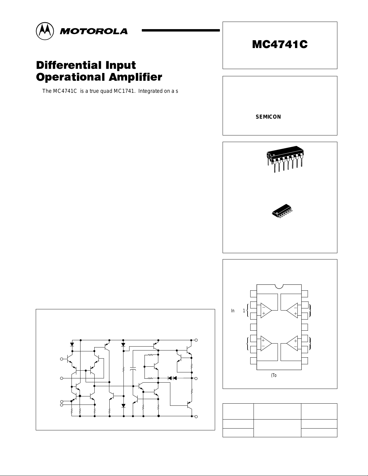
Representative Schematic Diagram
(1/4 of Circuit Shown)
Noninverting
Input
Inverting
Input
Offset
Null
1.0 k 1.0 k50 k
39 k
5.0 k
30 pF
MOTOROLA ANALOG IC DEVICE DATA
4.5 k
7. 5k
50 k 50
V
G
25
Output
50
V
CC
EE
PIN CONNECTIONS
Out 1
Inputs 1
V
CC
Inputs 2
Out 2
1
2
*
1
)
3
4
5
)
2
*
6
7
(Top View)
14
Out 4
13
*
4
)
)
3
*
12
11
10
9
8
Inputs 4
V
EE
Inputs 3
Out 3
ORDERING INFORMATION
Operating
Device
MC4741CD
MC4741CP
Motorola, Inc. 1996 Rev 5
Temperature Range
TA = 0° to +70°C
Package
SO–14
Plastic DIP
1
Page 2
MC4741C
MAXIMUM RATINGS (T
Power Supply Voltage V
Input Differential Voltage V
Input Common Mode Voltage V
Output Short Circuit Duration t
Operating Ambient Temperature Range T
Storage Temperature Range T
Junction Temperature T
= +25°C, unless otherwise noted.)
A
Rating Symbol Value Unit
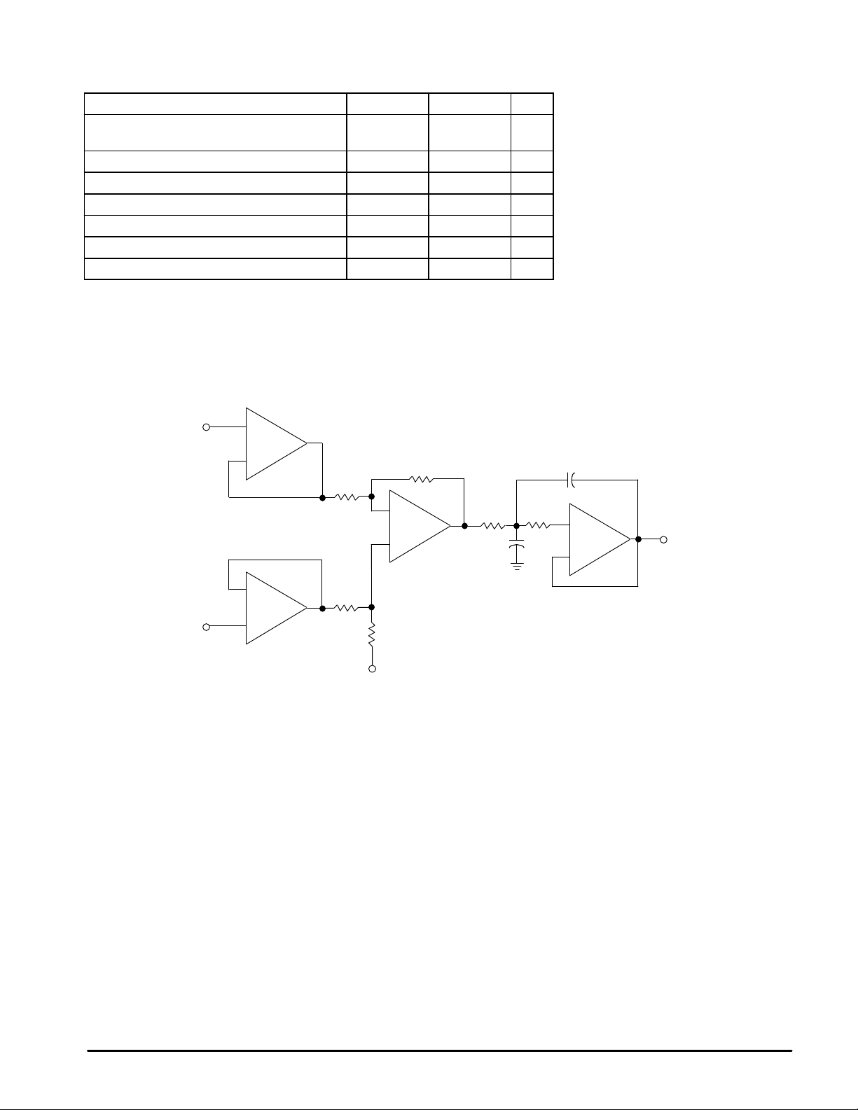
High Impedance Instrumentation Buffer/Filter
+
1/4
MC4741C
–
R1
V
CC
EE
ID
ICM
SC
A
stg
J
+18
–18
±36 V
±18 V
Continuous
0 to +70 °C
–55 to +125 °C
150 °C
R4
Vdc
C1
V
ID
–
1/4
MC4741C
+
R2
–
1/4
MC4741C
+
R3
R5 56
C2
+
1/4
MC4741C
–
2
MOTOROLA ANALOG IC DEVICE DATA
Page 3

MC4741C
ELECTRICAL CHARACTERISTICS (V
Characteristic
Input Offset Voltage (RS ≤ 10 k) V
Input Offset Current I
Input Bias Current I
Input Resistance r
Input Capacitance C
Offset Voltage Adjustment Range V
Common Mode Input Voltage Range V
Large Signal Voltage Gain (VO = ±10 V, RL ≥ 2.0 k) A
Output Resistance r
Common Mode Rejection (RS ≤ 10 k) CMR 70 90 – dB
Supply Voltage Rejection Ratio (RS ≤ 10 k) PSRR – 30 150 µV/V
Output Voltage Swing V
(RL ≥ 10 k) ±12 ±14 –
(RL ≥ 2 k) ±10 ±13 –
Output Short Circuit Current I
Supply Current – (All Amplifiers) I
Power Consumption (All Amplifiers) P
Transient Response (Unity Gain – Non–Inverting)
(VI = 20 mV, RL ≥ 2 kΩ, CL ≤ 100 pF) Rise Time t
(VI = 20 mV, RL ≥ 2 kΩ, CL ≤ 100 pF) Overshoot os – 15 – %
(VI = 10 V, RL ≥ 2 kΩ, CL ≤ 100 pF) Slew Rate SR – 0.5 – V/µs
= +15 V, VEE = –15 V, TA = 25°C, unless otherwise noted.)
CC
Symbol Min Typ Max Unit
IO
IO
IB
i
i
IOR
ICR
v
o
O
SC
D
C
TLH
– 2.0 6.0 mV
– 20 200 nA
– 80 500 nA
0.3 2.0 – MΩ
– 1.4 – pF
– ±15 – mV
±12 ±13 – V
20 200 – V/mV
– 75 – Ω
– 20 – mA
– 3.5 7.0 mA
– 105 210 mW
– 0.3 – µs
V
ELECTRICAL CHARACTERISTICS (V
Characteristic
Input Offset Voltage (RS ≤ 10 kΩ) V
Input Offset Current (TA = 0° to + 70°C) I
Input Bias Current (TA = 0° to + 70°C) I
Large Signal Voltage Gain (RL ≥ 2k, V
Output Voltage Swing (RL ≥ 2 k) V
*T
= 70°C T
high
low
= –0°C
OUT
= +15 V, VEE = –15 V, TA = * T
CC
= ±10 V) A
to T
high
Symbol Min Typ Max Unit
IO
IO
IB
V
O
, unless otherwise noted.)
low
– – 7.5 mV
– – 300 nA
– – 800 nA
15 – – V/mV
±10 ±13 – V
MOTOROLA ANALOG IC DEVICE DATA
3
Page 4

pp
Figure 1. Power Bandwidth
(Large Signal Swing versus Frequency)
28
24
20
MC4741C
Figure 2. Open Loop Frequency Response
120
100
80
16
12
Voltage Follower
8.0
, OUTPUT VOLT AGE (V )
O
V
THD < 5%
4.0
0
10 100 1.0 k 10 k 100 k
f, FREQUENCY (Hz)
Figure 3. Positive Output Voltage Swing
versus Load Resistance
15
14
13
12
pp
11
10
9.0
8.0
7.0
6.0
5.0
, OUTPUT VOLT AGE (V )
4.0
O
V
3.0
2.0
1.0
100 200 500 700 1.0 k 2.0 k 5.0 k 7.0 k 10 k
RL, LOAD RESISTANCE (
±
15 V Supplies
±
Ω
)
12 V
±
9.0 V
±6.0 V
60
40
VOLTAGE GAIN (dB)A
,
20
VOL
0
–20
1.0 10 100 1.0 k 10 k 100 k 1.0 M 10 M
f, FREQUENCY (Hz)
Figure 4. Negative Output Voltage Swing
versus Load Resistance
–15
–14
–13
–12
pp
–11
–10
–9.0
–8.0
–7.0
–6.0
–5.0
, OUTPUT VOLT AGE (V )
–4.0
O
V
–3.0
–2.0
–1.0
100 200 500 700 1.0 k 2.0 k 5.0 k 10 k7.0 k
RL, LOAD RESISTANCE (
±
15 V Supplies
±
Ω
)
12 V
±
9.0 V
±6.0 V
Figure 5. Output V oltage Swing versus
Load Resistance (Single Supply Operation)
28
30 V Supply
)
26
pp
24
27 V
22
24 V
20
18
21 V
16
18 V
14
12
15 V
10
8.0
6.0
OUTPUT VOL TAGE SWING (V
4.0
,V
O
2.0
12 V
9.0 V
6.0 V
5.0 V
0
0 1.0 2.0
3.0
4.0 5.0 6.0 7.0 8.0 9.0 10
RL, LOAD RESISTANCE (kW)
4
Figure 6. Noninverting Pulse Response
Output
5.0 V/DIV
Input
10 µs/DIV
MOTOROLA ANALOG IC DEVICE DATA
Page 5

MC4741C
Figure 7. Bi–Quad Filter
R
C1
V
in
For: Where:
fo = 1.0 kHz
Q = 10
TBP = 1
TN = 1
R2
V
ref
C
–
1/4
MC4741C
+
R2
TBP = center frequency gain
TN = passband notch gain
R1
Figure 8. Open Loop Voltage Gain
versus Supply V oltage
105
100
95
90
85
, VOLTAGE GAIN (dB)
80
V
A
75
70
0 2.0 4.0 6.0 8.0 10 12 14 16 18 20
VCC, |VEE|, SUPPLY VOLTAGES (V)
V
ref
Bandpass
Output
C
–
1/4
MC4741C
+
V
ref
R
100 k
100 k
R3
–
1/4
MC4741C
+
V
ref
–
1/4
MC4741C
+
C1
Notch Output
Figure 9. Transient Response Test Circuit
To Scope
(Input)
–
+
R
L
1
fo =
π
RC
2
R1 = QR
R1
R2 =
T
BP
R3 = TNR2
C1 = 10 C
V
= V
ref
R = 160 k
C = 0.001 µF
R1 = 1.6 M
R2 = 1.6 M
R3 = 1.6 M
C
L
1
CC
2
Ω
Ω
Ω
Ω
To Scope
(Output)
Figure 10. Absolute Value DVM Front End
900 k
+
1/4
MC4741C
100 k
V
500 k
V
–
CC
EE
1.0 k
1.0 M
Bridge Null Adjust
MOTOROLA ANALOG IC DEVICE DATA
1.0 k
MSD6150
MSD6102
–
1/4
MC4741C
+
1.0 k
0.5 µF
500 k
1.0 M
47 k
MC4741 Quad Op Amp
500 k
–
MC4741C
+
–
1/4
MC4741C
+
+
Polarity
–
1
2
MC1505
1/4
Common Mode Adjust
5
Page 6

14 8
17
A
F
HG D
–A–
14 8
G
–T–
SEATING
PLANE
D 14 PL
0.25 (0.010) A
N
SEATING
PLANE
–B–
71
K
M
T
B
C
K
P 7 PL
C
S
B
MC4741C
OUTLINE DIMENSIONS
P SUFFIX
PLASTIC PACKAGE
CASE 646–06
ISSUE L
L
J
M
D SUFFIX
PLASTIC PACKAGE
CASE 751A–03
ISSUE F
(SO–14)
M
0.25 (0.010) B
X 45
R
S
M
_
M
NOTES:
1. LEADS WITHIN 0.13 (0.005) RADIUS OF TRUE
POSITION AT SEATING PLANE AT MAXIMUM
MATERIAL CONDITION.
2. DIMENSION L TO CENTER OF LEADS WHEN
FORMED PARALLEL.
3. DIMENSION B DOES NOT INCLUDE MOLD
FLASH.
4. ROUNDED CORNERS OPTIONAL.
DIM MIN MAX MIN MAX
A 0.715 0.770 18.16 19.56
B 0.240 0.260 6.10 6.60
C 0.145 0.185 3.69 4.69
D 0.015 0.021 0.38 0.53
F 0.040 0.070 1.02 1.78
G 0.100 BSC 2.54 BSC
H 0.052 0.095 1.32 2.41
J 0.008 0.015 0.20 0.38
K 0.115 0.135 2.92 3.43
L 0.300 BSC 7.62 BSC
M 0 10 0 10
____
N 0.015 0.039 0.39 1.01
NOTES:
1. DIMENSIONING AND TOLERANCING PER ANSI
Y14.5M, 1982.
2. CONTROLLING DIMENSION: MILLIMETER.
3. DIMENSIONS A AND B DO NOT INCLUDE
MOLD PROTRUSION.
4. MAXIMUM MOLD PROTRUSION 0.15 (0.006)
PER SIDE.
5. DIMENSION D DOES NOT INCLUDE DAMBAR
PROTRUSION. ALLOWABLE DAMBAR
PROTRUSION SHALL BE 0.127 (0.005) TOTAL
IN EXCESS OF THE D DIMENSION AT
MAXIMUM MATERIAL CONDITION.
F
J
DIM MIN MAX MIN MAX
A 8.55 8.75 0.337 0.344
B 3.80 4.00 0.150 0.157
C 1.35 1.75 0.054 0.068
D 0.35 0.49 0.014 0.019
F 0.40 1.25 0.016 0.049
G 1.27 BSC 0.050 BSC
J 0.19 0.25 0.008 0.009
K 0.10 0.25 0.004 0.009
M 0 7 0 7
P 5.80 6.20 0.228 0.244
R 0.25 0.50 0.010 0.019
MILLIMETERSINCHES
INCHESMILLIMETERS
____
Motorola reserves the right to make changes without further notice to any products herein. Motorola makes no warranty , representation or guarantee regarding
the suitability of its products for any particular purpose, nor does Motorola assume any liability arising out of the application or use of any product or circuit, and
specifically disclaims any and all liability, including without limitation consequential or incidental damages. “T ypical” parameters which may be provided in Motorola
data sheets and/or specifications can and do vary in different applications and actual performance may vary over time. All operating parameters, including “Typicals”
must be validated for each customer application by customer’s technical experts. Motorola does not convey any license under its patent rights nor the rights of
others. Motorola products are not designed, intended, or authorized for use as components in systems intended for surgical implant into the body, or other
applications intended to support or sustain life, or for any other application in which the failure of the Motorola product could create a situation where personal injury
or death may occur. Should Buyer purchase or use Motorola products for any such unintended or unauthorized application, Buyer shall indemnify and hold Motorola
and its officers, employees, subsidiaries, affiliates, and distributors harmless against all claims, costs, damages, and expenses, and reasonable attorney fees
arising out of, directly or indirectly, any claim of personal injury or death associated with such unintended or unauthorized use, even if such claim alleges that
Motorola was negligent regarding the design or manufacture of the part. Motorola and are registered trademarks of Motorola, Inc. Motorola, Inc. is an Equal
Opportunity/Affirmative Action Employer.
How to reach us:
USA/EUROPE /Locations Not Listed: Motorola Literature Distribution; JAPAN: Nippon Motorola Ltd.; Tatsumi–SPD–JLDC, 6F Seibu–Butsuryu–Center,
P.O. Box 20912; Phoenix, Arizona 85036. 1–800–441–2447 or 602–303–5454 3–14–2 Tatsumi Koto–Ku, Tokyo 135, Japan. 03–81–3521–8315
MFAX: RMF AX0@email.sps.mot.com – TOUCHT ONE 602–244–6609 ASIA/ PACIFIC: Motorola Semiconductors H.K. Ltd.; 8B Tai Ping Industrial Park,
INTERNET: http://Design–NET.com 51 Ting Kok Road, Tai Po, N.T., Hong Kong. 852–26629298
6
◊
MOTOROLA ANALOG IC DEVICE DATA
MC4741C/D
*MC4741C/D*
 Loading...