

Datasheet MC4558IN, MC4558CN, MC4558CD, MC4558, MC4558ID Datasheet (SGS Thomson Microelectronics)
Page 1
DUALBIPOLAR OPERATIONAL AMPLIFIERS
.INTERNALLY COMPENSATED
.SHORT–CIRCUIT PROTECTION
.GAIN AND PHASE MATCH BETWEEN
AMPLIFIERS
.LOW POWER CONSUMPTION
.PIN TO PINCOMPATIBLE WITH
MC1458/LM358
.GAIN BANDWIDTH PRODUCT (at 100kHz)
5.5MHz
WIDE BANDWIDTH
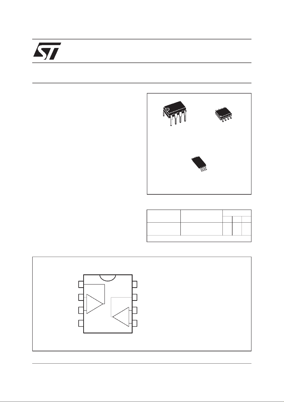
N
DIP8
(PlasticPackage)
(Thin Shrink Small Outline Package)
(PlasticMicropackage)
P
TSSOP8
MC4558
D
SO8
DESCRIPTION
TheMC4558 isa highperformancemonolithicdual
operationalamplifier.
Thecircuit combines allthe outstandingfeaturesof
theMC1458and,inaddition,possessesthreetimes
theunity gain bandwidthof the industrystandard.
PIN CONNECTIONS (top view)
1
2
3
45
-
+
-
+
ORDER CODES
Part
Number
MC4558C 0
MC4558I -40
Example : MC4558CN
8
7
6
1– Output1
2– Invertinginput 1
3– Non-inverting input 1
4–V
5– Non-inverting input 2
6– Invertinginput 2
7– Output2
8– V
CC
CC
-
+
Temperature
Range
o
C, +70oC •••
o
C, +105oC •••
Pakcage
NDP
August1998
1/7
Page 2
MC 4558
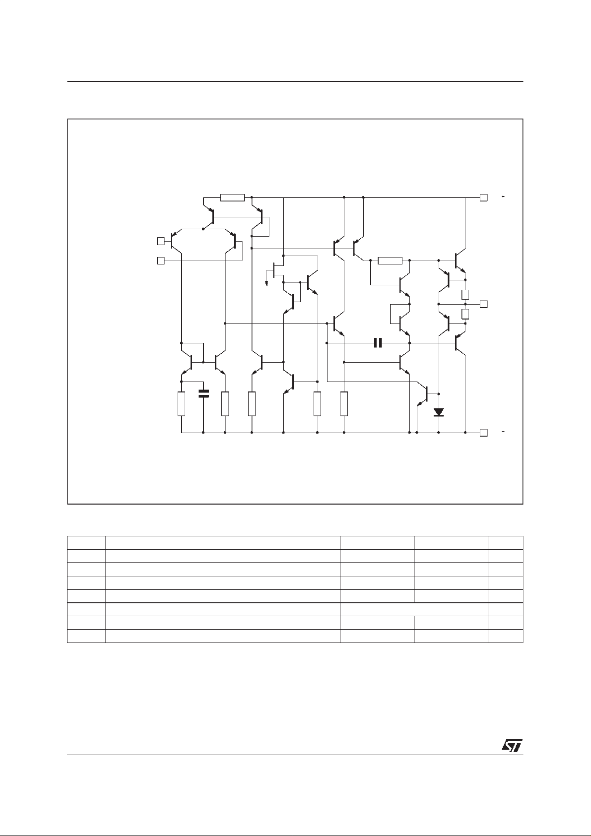
SCHEMATIC DIAGRAM (1/2 MC4558)
Invertinginput
Non-inverting input
7.1kΩ
87pF
3.1kΩ
7.1kΩ
480Ω
4.2kΩ
36kΩ
10pF
150Ω
25Ω
25Ω
V
CC
Output
V
CC
ABSOLUTE MAXIMUM RATINGS
Symbol Parameter MC4558I MC4558C Unit
V
P
T
T
2/7
Supply Voltage ±22 ±22 V
CC
Input Voltage ±15 ±15 V
V
i
Differential Input Voltage ±30 ±30 V
V
id
Power Dissipation 680 680 mW
tot
Output Short-circuit Duration Infinite
Operating Free-air Temperature Range –40 to +105 0 to +70
oper
Storage Temperature Range –65 to +150 –65 to +150
stg
o
C
o
C
Page 3
MC4558
ELECTRICAL CHARACTERISTICS
= ±15V, T
V
CC
Symbol Parameter Min. Typ. Max. Unit
V
A
Input Offset Voltage (RS≤ 10 kΩ)
io
Input Offset Current
I
io
Input Bias Current
I
ib
Large Signal Voltage Gain (VO= ±10V, RL=2kΩ)
vd
SVR Supply Voltage Rejection Ratio (R
I
V
Supply Current, all Amp, no Load
CC
Input Common Mode Voltage Range
icm
CMR Common-mode Rejection Ratio (R
I
Output Short-circuit Current 10 20 40 mA
os
V
Output Voltage Swing
o
SR Slew Rate
(V
t
Rise Time
r
(V
K
R
Overshoot
OV
(V
R
Input Resistance 0.3 2 MΩ
i
Input Capacitance 1.4 pF
C
i
Output Resistance 75 Ω
O
B Unity Gain Bandwidth 2.8 MHz
GBP Gain Bandwidth Product
(V
THD Total Harmonic Distortion
(f = 1kHz, A
V
O1/VO2
e
Equivalent Input Noise Voltage (f = 1kHz, Rs= 100Ω)12
n
Channel Separation 120 dB
=25oC (unless otherwise specified)
amb
=25oC
T
amb
≤ T
≤ T
≤ T
≤ T
≤ T
≤ T
≤ T
≤ T
≤ T
≤ T
max
max
max
max.
max.
max.
max.
max
max.
.
.
.
≤ 10kΩ)
S
≤ 10kΩ)
S
.
= 10kΩ
L
=2kΩ
R
L
RL= 10kΩ
=2kΩ
R
L
=25oC, unity gain) 1.5 2.2
amb
=25oC, unity gain) 0.3
amb
=25oC, unity gain) 15
amb
=25oC) 5.5
amb
=25oC) 0.008
amb
T
min.
amb
=25oC
T
amb
. ≤ T
T
min
amb
=25oC
T
amb
≤ T
T
min.
amb
=25oC
T
amb
≤ T
T
min.
amb
=25oC
T
amb
. ≤ T
T
min
amb
=25oC
T
amb
. ≤ T
T
min
amb
=25oC
T
amb
≤ T
T
min.
amb
=25oC
T
amb
. ≤ T
T
min
amb
=25oCR
T
amb
≤ T
T
min.
amb
= ±10V, RL=2kΩ,CL= 100pF, T
I
= ±20mV, RL=2kΩ,CL= 100pF, T
I
= ±20 mV, RL=2kΩ,CL= 100pF, T
I
= 10mV, RL=2kΩ,CL= 100pF,f = 100kHz, T
I
= 20dB, RL=2kΩ,Vo=2Vpp,CL= 100pF, T
v
50
25
77
77
±12
±12
70
70
±12
±10
±12
±10
15
6
20 100
200
50 400
500
V/mV
200
90
2.3 4.5
6
90
±14
±13
V/µs
MHz
√Hz
mV
nA
nA
dB
mA
V
dB
V
µs
%
%
nV
3/7
Page 4

MC 4558
TRANSIENT RESPONSE TEST CIRCUIT
OSCILLOSCOPE
V
I
OSCILLOSCOPE
R
L
C
L
4/7
Page 5

PACKAGE MECHANICAL DATA
8 PINS – PLASTICDIP
MC4558
Dimensions
Min. Typ. Max. Min. Typ. Max.
Millimeters Inches
A 3.32 0.131
a1 0.51 0.020
B 1.15 1.65 0.045 0.065
b 0.356 0.55 0.014 0.022
b1 0.204 0.304 0.008 0.012
D 10.92 0.430
E 7.95 9.75 0.313 0.384
e 2.54 0.100
e3 7.62 0.300
e4 7.62 0.300
F 6.6 0260
i 5.08 0.200
L 3.18 3.81 0.125 0.150
Z 1.52 0.060
PM-DIP8.EPS
DIP8.TBL
5/7
Page 6

MC 4558
PACKAGE MECHANICAL DATA
8 PINS – PLASTICMICROPACKAGE(SO)
Dimensions
Min. Typ. Max. Min. Typ. Max.
Millimeters Inches
A 1.75 0.069
a1 0.1 0.25 0.004 0.010
a2 1.65 0.065
a3 0.65 0.85 0.026 0.033
b 0.35 0.48 0.014 0.019
b1 0.19 0.25 0.007 0.010
C 0.25 0.5 0.010 0.020
c1 45
o
(typ.)
D 4.8 5.0 0.189 0.197
E 5.8 6.2 0.228 0.244
e 1.27 0.050
e3 3.81 0.150
F 3.8 4.0 0.150 0.157
L 0.4 1.27 0.016 0.050
M 0.6 0.024
S8
o
(max.)
PM-SO8.EPS
SO8.TBL
6/7
Page 7

PACKAGE MECHANICAL DATA
8 PINS – THIN SHRINK SMALL OUTLINE PACKAGE
MC4558
Dim.
Min. Typ. Max. Min. Typ. Max.
Millimeters Inches
A 1.20 0.05
A1 0.05 0.15 0.01 0.006
A2 0.80 1.00 1.05 0.031 0.039 0.041
b 0.19 0.30 0.007 0.15
c 0.09 0.20 0.003 0.012
D 2.90 3.00 3.10 0.114 0.118 0.122
E 6.40 0.252
E1 4.30 4.40 4.50 0.169 0.173 0.177
e 0.65 0.025
k0
o
o
8
o
0
o
8
l 0.50 0.60 0.75 0.09 0.0236 0.030
Information furnished is believed to be accurate and reliable. However, STMicroelectronics assumes no responsibility for the
consequences of use of such information nor for any infringement of patents or other rights of third parties which may result
from its use. No license is granted by implication or otherwise under any patent or patent rights of STMicroelectronics. Specifications mentioned in this publication are subject to change without notice. This publication supersedes and replaces all information previously supplied. STMicroelectronics products are not authorized for use as critical components in life support
devices or systems without express written approval of STMicroelectronics.
The ST logo is a trademark of STMicroelectronics
1998 STMicroelectronics – Printed in Italy – All Rights Reserved
STMicroelectronics GROUP OF COMPANIES
Australia - Brazil - Canada - China - France - Germany - Italy - Japan - Korea - Malaysia - Malta - Mexico - Morocco
The Netherlands - Singapore - Spain - Sweden - Switzerland - Taiwan - Thailand - United Kingdom - U.S.A.
ORDERCODE :
7/7
 Loading...