

Page 1
SEMICONDUCTOR
TECHNICAL DATA
PLL TUNING CIRCUIT
PIN CONNECTIONS
(16 Pin TSSOP)
Order this document by MC44871/D
116
15
14
13
12
11
10
9
2
3
4
5
6
7
8
V
TUN
CP
HF1
B2
B1
B0
Amp In
B4
DTB SUFFIX
PLASTIC PACKAGE
CASE 948F
(TSSOP–16)
16
1
HF2
Gnd
Xtal
SCL
SDA
ADD
V
CC
ADC
(Top View)
WITH HIGH SPEED I2C BUS
AND 30 V TUNING SUPPLY
1
MOTOROLA ANALOG IC DEVICE DATA
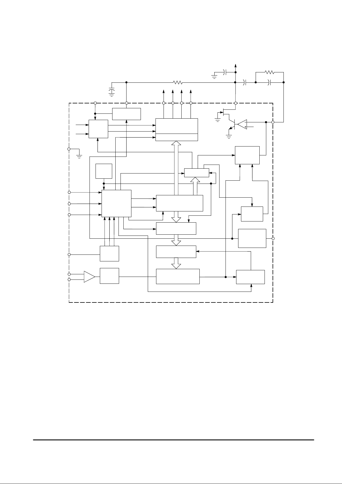
The MC44871 is a tuning circuit for TV, VCR and Multimedia tuner
applications. This device contains on one chip all the functions required for
PLL control of a VCO. This integrated circuit also contains a high frequency
prescaler and thus can handle frequencies up to 1.3 GHz.
The MC44871 has an integrated dc/dc converter to generate the 30 V
supply voltage for the tuning amplifier on the chip. A tuner using the
MC44871 does not require an external 30 V supply.
The MC44871 is controlled by a I2C bus, and has a chip address function.
The MC44871 data format is the same as the MC44818.
The MC44871 is manufactured on a single silicon chip using Motorola’s
high density bipolar process, MOSAIC (Motorola Oxide Self Aligned
Implanted Circuits).
• The Pin Called V
CC2
for the MC44818 is Now Called CP (Charge
Pump). This Pin is the Output of the DC/DC Converter; a 1.0 nF
Capacitor Replaces the Need for an External 30 V Supply
• High Speed I
2
C Bus (up to 800 kHz)
• I
2
C Bus Read Mode for Lock Detector and AFC Level
• HF Input is Balanced
• MC44871 has Three PNP High Current (30 mA) Band Buffers (B0, B1,
B2) and One NPN Low Current (5.0 mA) Band Buffer (B4)
• V
CC
Internally Supplies PNP Band Buffers
• The Tuning Voltage is Generated Through an External Pull–Up
Resistor (750 kΩ)
• Less Phase Comparator Output Current
• Single 5.0 V Supply Operation
MOSAIC is a trademark of Motorola, Inc.
ORDERING INFORMATION
Device
Operating
Temperature Range
Package
MC44871DTB TA = –20° to +85°C TSSOP–16
This document contains information on a new product. Specifications and information herein
are subject to change without notice.
Motorola, Inc. 1998 Rev 1
Page 2
MC44871
2
MOTOROLA ANALOG IC DEVICE DATA
92
CP
687115.0 V
Figure 1. Representative Block Diagram
This device contains 3,204 active transistors.
Gnd
Test
Logic
Buffers
Latches
P–On
Reset
I2C Bus
Receiver
Latches
Phase
Comp
Ref
Divider
Latch Control
Program Divider
15 Bit
Latches B
Latches A
÷
8
Prescaler
Preamp
DTB2
POR
Operational
Amplifier
V
ref
DTB1
CLO
Data
RL
DTF
F
out
TDI
F
out
F
ref
T10, T11
T14
T13
4
6
15
1
F
out
F
ref
5
13
14
12
4
SDA
SCL
ADD
HF2
V
CC
V
TUN
Amp In
Xtal
B4 B2 B1 B0
DTS
512/1024
16
15
Shift Register
15 Bit
Approximate values of the external components for generation of the tuning voltage are:
C1 = 1.0 nF Charge Pump filter capacitor
R1 = 750 kΩ (560 kΩ minimum) Pull–up resistor
C4 = 330 pF V
TUN
filter capacitor
C2 = 47 nF, C3 = 22 nF, R2 = 39 kΩ Loop filter
These component values depend on the application.
ADC
10
ADC
3.2 or 4.0 MHz
Osc
3
HF1
C1
R1
C4
C3
R2
V
TUN
C2
Bands Out
DC/DC
Converter
Page 3
MC44871
3
MOTOROLA ANALOG IC DEVICE DATA
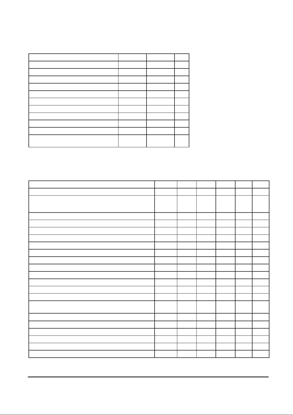
MAXIMUM RATINGS (Maximum ratings are those values beyond which
permanent damage to the device may occur. Exposure to those limits may also affect device
reliability; TA = 25°C, unless otherwise noted.)
Rating
Pin Value Unit
Power Supply Voltage (VCC) 11 6.0 V
Storage Temperature – –65 to +150 °C
Operating Temperature Range – –20 to +85 °C
Operational Amplifier Output Voltage 1 40 V
RF Input Level 80 MHz to 1.3 GHz 3, 4 1.5 Vrms
NPN Band Buffer ”Off” Voltage 9 10 V
NPN Band Buffer ”On” Current 9 15 mA
PNP Band Buffer “Off” V oltage 6, 7, 8 6.0 V
PNP Band Buffer “On” Current 6, 7, 8 50 mA
PNP Band Buffer – Short Circuit Duration (Note 1) 6, 7, 8 Continuous –
Band Buffer Operation at 40 mA 6, 7, 8 10 s
all PNP Buffers “On”
NOTES: 1. At VCC = 5.0 V and TA = –20° to +80°C one buffer “On” only.
2.ESD data available upon request.
ELECTRICAL CHARACTERISTICS (Parameter Type: A–100% Tested, B–100% Correlation T ested, C–Characterized on
Samples, D–Design Parameter, VCC = 5.0 V , TA = 25°C, unless otherwise specified, 750 kΩ pull–up resistor between CP [Pin2] and
V
TUN
[Pin 1].)
Characteristic
Pin Min Typ Max Unit Type
VCC Supply Voltage Range 11 4.5 5.0 5.5 V A
VCC Supply Current (All Buffers “Off”)
– 35 45
A
One Buffer “On” when Open 11 – 40 50 mA B
One Buffer “On” at 40 mA – 80 90 B
PNP Band Buffer B0, B1, B2 Leakage Current when “Off” 6, 7, 8 – 0.01 1.0 µA A
PNP Band Buffer B0, B1, B2 Saturation Voltage when “On” at 30 mA 6, 7, 8 – 200 500 mV B
NPN Band Buffer B4 Leakage Current when “Off” 9 – 0.01 1.0 µA A
NPN Band Buffer ”Off” Voltage 9 0 – 5.5 V D
NPN Band Buffer B4 Saturation Voltage when “On” at 1.0 µA 9 – 50 100 mV A
NPN Band Buffer B4 Voltage when ”On” @ 5.0 mA 9 – 1.2 1.6 V A
Reference Oscillator Frequency Range 15 3.15 3.2 4.05 MHz D
Phase Comparator 3–State Current 16 –15 0 15 nA A
Phase Comparator Output Current – High Value 16 12 20 28 µA A
Phase Comparator Output Current – Low Value 16 2.0 6.0 10 µA A
DC–DC Converter Output Voltage, Sourcing 50 µA 2 28 31 34.5 V A
DC–DC Converter Maximum Current, Output Short Circuited 2 – 200 350 µA A
DC–DC Converter setting time from VCC >4.5 V to DC–DC Converter
Voltage > 28 V @ Load = 750 kΩ/1.0 nF
2 – – 25 ms C
Operational Amplifier Internal Reference Voltage (V
ref
) – 1.3 1.9 2.5 V A
Operational Amplifier Input Current 16 –15 0 15 nA A
Operational Amplifier DC Open Loop Gain – 100 300 – – A
Operational Amplifier Gain Bandwidth Product (CL = 1.0 nF) – 0.3 – – MHz D
Operational Amplifier Low Output Voltage, Sinking 50 µA 16 – 0.2 0.4 V D
Oscillator – Negative Resistance 15 1.0 – – kΩ D
Page 4
MC44871
4
MOTOROLA ANALOG IC DEVICE DATA
PIN FUNCTION DESCRIPTION (see Figure 1)
Pin Symbol Description
1 V
TUN
Operational amplifier output which provides the tuning voltage
2 CP DC–DC Converter output (Charge Pump)
3, 4 HF1, HF2 Symmetrical HF inputs
5 Gnd Ground
6, 7, 8 B2, B1, B0 PNP Band Buffer outputs
9 B4 NPN Band Buffer output
10 ADC Three bit ADC for Automatic Frequency Tuning, readable through the bus
11 V
CC
Positive supply of the circuit (5.0 V)
12 ADD Chip address function
13 SDA I2C bus Data Input/Output
14 SCL I2C bus Clock
15 Xtal Crystal Oscillator (3.2 MHz or 4.0 MHz)
16 Amp In Operational amplifier input
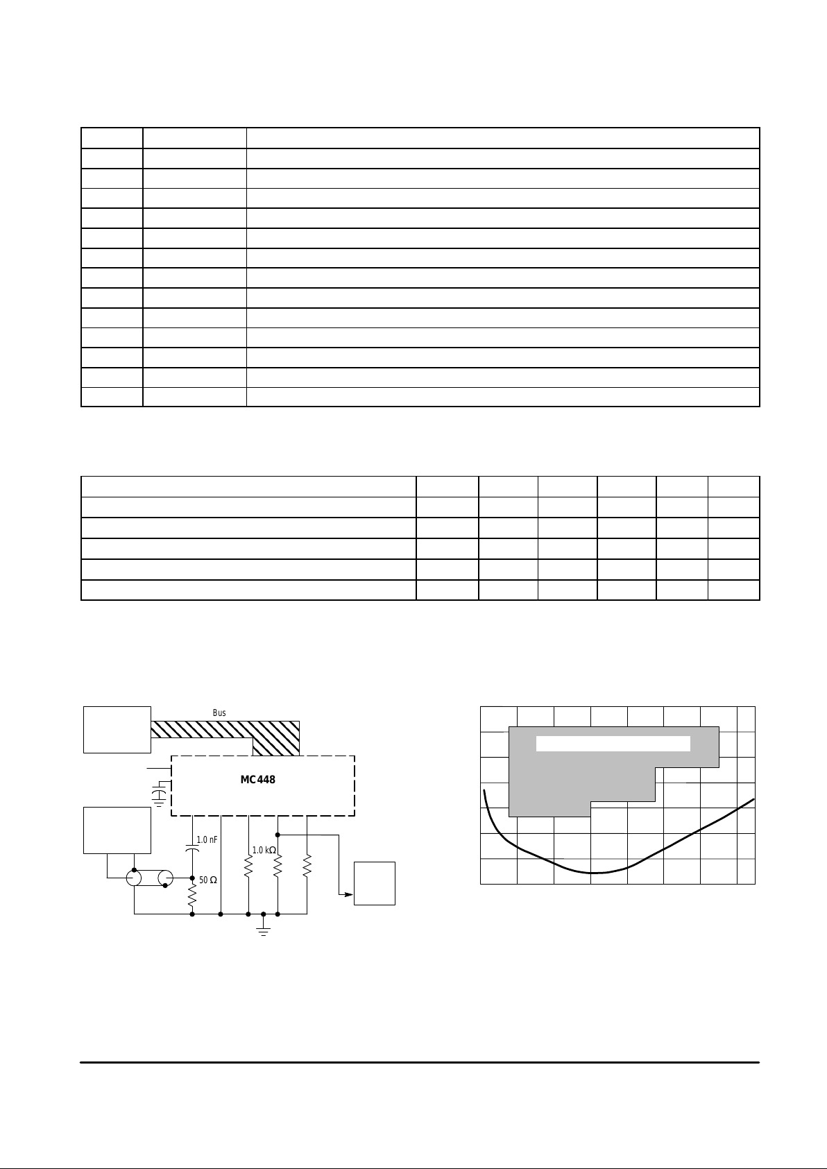
HF INPUT SENSITIVITY AND OVERLOAD CHARACTERISTICS (V
CC
= 5.0 V , TA = 25°C.) (See Figure 2.)
Characteristics
Pin Min Typ Max Unit Type
DC Bias (Internal) 3, 4 – 1.6 – V A
80–150 MHz 3, 4 10 – 315 mVrms C
150–600 MHz 3, 4 5.0 – 315 mVrms C
600–950 MHz 3, 4 10 – 315 mVrms C
950–1300 MHz 3, 4 50 – 315 mVrms C
50 Ω Cable
Figure 2. HF Sensitivity Test Circuit
NOTE: 1.Device is in test mode. B1, B2 are “On” and B0, B4 are “Off”.
Sensitivity is level of HF generator on 50 Ω load.
13 14
HF13Gnd5B08B17B26B4
9
Bus Controller
HF Generator
HF Out Gnd
11VCC = 5.0 V
Counter
In
Bus
1.0 k
Ω
50
Ω
1.0 nF
MC44871
4
1.0 nF
1.0 k
Ω
1.0 k
Ω
Guaranteed Sensitivity Performance
RF LEVEL (dBm)
FREQUENCY (MHz)
Figure 3. Typical HF Sensitivity Performance
(VCC = 5.0 V, Temperature = 25°C)
10
0
–10
–20
–30
–40
–50
–60
0 200 400 600 800 1000 1200 1400
Page 5

MC44871
5
MOTOROLA ANALOG IC DEVICE DATA
16 Amp In
Negative input of operational
amplifier and phase detector
charge pump output
15 Xtal
Crystal oscillator
(3.2 MHz or 4.0 MHz)
14 SCL
Clock input (I2C bus)
13 SDA
Data input/output (I2C bus)
12 ADD
Chip Address
11 V
CC
Positive supply of the
circuit (5.0 V)
10 ADC
Three bit control for AFC
9 B4
NPN Buffer
B0 8
Figure 4. Pin Circuit Schematic
V
TUN
1
Operational amplifier
output which provides
the tuning voltage
CP 2
Converter output
(Charge Pump)
HF1 3
HF2 4
Gnd 5
Circuit ground
B2 6
B1 7
500
132 k
20 V
V
CC
96 k
96 k
1/2 V
CC
500
132 k
20 V
5.0 V
100
2.0 k10 k
20 V
20 V
20 V
50
20 V
20 V
6.0 k
Ω
5.0 V
5.0 V
5.0 V
2.0 k
2.0 k
1.2
…
1.8 V
5.0 V
5.0 V
“On”/“Off”
32 V
1
2
6
20 V
“On”/“Off”
“On”/“Off”
20 V
20 V
1.5 k
V
CC
ACK
V
CC
96 k
96 k
1/2 V
CC
V
CC
150 k
50 k
10 k
20 V
10 k
20 V
V
CC
200
20 V
“On”/“Off”
Inputs to
presealer
PNP Band
Buffers
Page 6

MC44871
6
MOTOROLA ANALOG IC DEVICE DATA
HIGH SPEED I2C BUS (The circuit is controlled by a I
2
C bus with a Serial Data [SDA], Serial Clock [SCL], Chip Address
Control [ADD] inputs. The device I2C bus has a read mode [odd addresses] and a write mode [even addresses].
ELECTRICAL CHARACTERISTICS (V
CC
= 5.0 V , TA = 25°C, unless otherwise specified.)
Characteristic
Pin Symbol Min Typ Max Unit Type
SDA/SCL Output Current at 0 V 13, 14 – – 10 µA A
SDA/SCL Low Input Level 13, 14 V
IL
– – 1.5 V B
SDA/SCL High Input Level 13, 14 V
IH
3.0 – – V B
SDA/SCL Input Current for Input Level from 0.4 V to 0.3 V
CC
13, 14 –5.0 0 5.0 µA C
SDA/SCL Input Level 13, 14 0 – VCC +
0.3
V D
ADD Input Level 12 –0.01
V
CC
– 1.1 V
CC
D
SDA/SCL Capacitance 13, 14 C
i
– – 10 pF C
SDA Low Output Level (sinking 3.0 mA) 13 – 0.3 1.0 V A
SDA Low Output Level (sinking 15 mA) 13 – – 1.5 V C
TIMING CHARACTERISTICS
Characteristic Pin Symbol Min Typ Max Unit Type
Bus Clock Frequency 14 0 – 800 kHz C
Bus Free Time Between Stop and Start – T
buf
200 – – ns C
Setup Time for Start Conditions – T
su;sta
500 – – ns C
Hold Time for Start Condition – T
hd;sta
500 – – ns C
Data Setup Time – T
su;dat
0 – – ns C
Data Hold Time – T
hd;dat
0 – – ns C
Setup Time for Stop Condition – T
su;sto
500 – – ns C
Hold time for Stop Condition – T
hd;sto
500 – – ns C
Acknowledge Propagation Delay T
ack;low
– – 300 ns C
SDA Fall Time at 3.0 mA sink I and 130 pF Load 13 – – 50 ns C
SDA Fall Time at 3.0 mA sink I and 400 pF Load 13 – – 80 ns C
SDA/SCL Rise Time 13, 14 – – 300 ns C
SCL Fall Time 13, 14 – – 300 ns C
Pulse Width of Spikes Suppressed by the Input Filter 13,14 T
sp
– – 50 ns C
0 V
V
CC
V
IH
V
IL
Not Defined
T
buf
T
hd;dat
T
su;dat
T
su;stoThd;sta
T
ack:low
Start
Stop
T
su;sta
Chip address
T
hd;sto
Start
Stop
SDA
SCL
SDA
SCL
SDA
SCL
ACK
Timings Definition
Levels Definition
Page 7

MC44871
7
MOTOROLA ANALOG IC DEVICE DATA
Figure 5. High Speed I2C Compatible Bus Data Format
12345678910 1819
STA Chip Address ($C2) First Byte Stop
ACKACKACK
SCL
SDA
2 or 4 Data Bytes
I2C Write Mode Format and Bus Receiver
The incoming information, consisting of a chip address
byte followed by two or four data bytes, is treated in the I2C
bus receiver. The definition of the permissible bus protocol is
shown below:
1_ST A CA CO BA FM FL STO
2_ST A CA FM FL CO BA STO
3_ST A CA CO BA STO
4_ST A CA FM FL STO
STA = Start Condition
CA = Chip Address Byte
CO = Control Information
BA = Band Information
FM = Frequency Information with MSB
FL = Frequency Information with LSB
STO = Stop Condition
Figure 5 shows the five bytes of information that are
needed for circuit operation: the chip address, two bytes of
control and information, and two bytes of frequency
information.
After the chip address, two or four data bytes may be
received: if three data bytes are received, the third one is
ignored. If five or more data bytes are received, the fifth and
following ones are ignored, and the last acknowledge pulse is
sent at the end of the fourth data byte.
The first and the third data bytes contain a function bit
which allows the IC to distinguish between frequency
information and control plus band information. If the function
bit is logic “1”, the two following bytes contain control and
band information. The first data byte, after the chip address,
may be byte CO or byte FM. The two bytes of frequency
information are preceeded by a logic “0”.
Chip Address
Even addresses are for write mode, and odd addresses
are for read mode. Chip address is programmable by Pin 12
(ADD).
ADD Pin 12 Address (HEX.)
–0.01 VCC to 0.1 V
CC
C0/C1
0.2 VCC to 0.3 VCC (or Open) C2/C3
0.4 VCC to 0.7 V
CC
C4/C5
0.8 VCC to 1.1 V
CC
C6/C7
Page 8

MC44871
8
MOTOROLA ANALOG IC DEVICE DATA
The Two Permissible Protocols with Five Bytes
CA_Chip Address 1 1 0 0 0 0/1 0/1 0 ACK
CO_Control Information 1 T14 T13 T12 T11 T10 T9 T8 ACK
BA_Band Information X X X B4 X B2 B1 B0 ACK
FM_Frequency Information 0 N14 N13 N12 N11 N10 N9 N8 ACK
FL_Frequency Information N7 N6 N5 N4 N3 N2 N1 N0 ACK
CA_Chip Address 1 1 0 0 0 0/1 0/1 0 ACK
FM_Frequency Information 0 N14 N13 N12 N11 N10 N9 N8 ACK
FL_Frequency Information N7 N6 N5 N4 N3 N2 N1 N0 ACK
CO_Control Information 1 T14 T13 T12 T11 T10 T9 T8 ACK
BA_Band Information X X X B4 X B2 B1 B0 ACK
I2C Read Mode Format
The incoming information consists of the chip address
byte in read mode (odd address). The device then answers
with an acknowledge followed by a byte containing lock and
ADC information. There is no ACK pulse sent after this byte.
1_STA CA ADC_LO
ADC_LO = ADC and Lock information
I2C Read Format
CA_Chip Address 1 1 0 0 0 0/1 0/1 1 ACK
ADC_LO 1 LO X X X AD2 AD1 AD0 (no ACK)
Definition of the Bits for Test and Features
Bits B0, B1, B2: Control the PNP Band Buffers
B0, B1, B2 = 0 Buffer is “Off”, Output Low
= 1 Buffer is “On”, Output High
Bit B4: Controls the NPN Band Buffer
B4 = 0 Buffer is “Off”, Output High
= 1 Buffer is “On”, Output Low
Bit T8: Controls the Operational Amplifier Output
T8 Operation
T8 = 0 Operational Amplifier Normal Operation
= 1 Output State of Operational Amplifier
Switched Off
Output Pulls High through External Resistor
Bit T10, T11: Control the Reference Divider
T10 T11 Divider Ratio
0 0 512
0 1 1024
1 0 1024
1 1 512
Bit T9, T12: Control the Phase Comparator
T9 T12 Function
0 0 Upper Source Only
0 1 Lower Source Only
1 0 Normal Operation
1 1 High Impedance
Page 9

MC44871
9
MOTOROLA ANALOG IC DEVICE DATA
Bit T13: Switches the Band Buffer Output to Test Mode
T13 = 0 Normal Operation
= 1 Test Mode: F
ref
Out at B2 F
by2
Out at B1
In the test mode, B2 and B1 have to be ON (B2=B1=1).
F
ref
is the reference frequency. F
by2
is the output frequency of
the programmable divider divided–by–2.
Bit T14: Controls the Charge Pump Current
T14 = 0 Pump Current 5.0 µA
= 1 Pump Current 20 µA
Bit AD2, AD1, AD0: Indicate the ADC Pin Analog Level
ADC Input Voltage AD2 AD1 AD0
0 to 0.18 V
CC
0 0 0
0.18 to 0.34 V
CC
0 0 1
0.34 to 0.5 V
CC
0 1 0
0.5 to 0.66 V
CC
0 1 1
0.66 to 0.82 V
CC
1 0 0
0.82 to 1.0 V
CC
1 0 1
Bit LO: Indicates the Status of Lock Detetector
LO = 0 PLL Status Not Locked
LO = 1 PLL Status Locked
Figure 6. Equivalent Circuit of the Integrated
PNP Band Buffers
“On”/“Off”
I
SUB
30 mA (40 mA
at 0 to 80
°
C)
I
B
Out
B0
…
B2
IB + I
SUB
= 5.5 mA Typical
IB = Base Current
I
SUB
= Substrate Current of PNP
Saturation Voltage
0.2 V Typical
0.5 V Max
V
CC
Out B4
VCC = 5.0 V
1.2 V typ
@ 5.0 mA
IB1 + IB2 + IB3 = 0.5 mA Typ
IB = Base Current
Protection 20...25 V
”On”/”Off”
200
I
B1
I
B2
I
B3
Figure 7. Equivalent Circuit of the Integrated
NPN Band Buffer
OPERA TING DESCRIPTION
Introduction
A representative block diagram and typical system
application are shown in Figures 1 and 8. A discussion of the
features and function of each of the internal blocks is given.
The Programmable Divider
The programmable divider is a presettable down counter.
When it has counted to zero it takes its required division ratio
out of the latches B. Latches B are loaded from latches A by
means of signal TDI which is synchronous to the
programmable divider output signal.
Since latches A receive the data asynchronously with the
programmable divider; this double latch scheme is needed to
assure correct data transfer to the counter.
The division ratio definition is given by:
N = 16384 x N14 + 8192 x N13 + … + 4 x N2 + 2 x N1 + N0
Maximum Ratio 32767 Minimum Ratio 256
N0 … N14 are the different bits for frequency information.
At power–on the whole bus receiver is reset and the
programmable divider is set to a counting ratio of N = 256 or
higher.
The Prescaler
The divide–by–8 prescaler has a preamplifier which
guarantees high input sensitivity.
The Phase Comparator
The phase comparator is both phase and frequency
sensitive and has very low output leakage current in the high
impedance state.
The Operational Amplifier
The operational amplifier is designed for very low noise,
low input bias current and high power supply rejection. The
positive input is biased internally. The operational amplifier
output (Pin 1) needs an external 750 kΩ pull–up resistor (560
kΩ minimum). This minimum value is defined by the charge
pump output current capability.
The Oscillator
The oscillator uses a 3.2 or a 4.0 MHz crystal tied to ground
in series with a capacitor. The crystal operates in the series
resonance mode.
The voltage at Pin 15 has low amplitude and low harmonic
distortion.
Power Dissipation
The typical power dissipation of the circuit is about
200 mW (V
TUN
= 15 V with external pull–up of 560 kΩ, one
buffer “On” at 30 mA). It is calculated with the following
formula:
PD
+
ǒ
VCCxI
CC
Ǔ
)
V
Pin2
*
V
TUN
560 k
W
xV
TUN
)
ǒ
V
sat
xI
Out
Ǔ
buffer
Example:(5x38))
32–15
5.6 x 10
5
x15
)(0.20 x 30)+
197 mW
Page 10

MC44871
10
MOTOROLA ANALOG IC DEVICE DATA
5
HF1
HF2
V
CC
5.0 V
÷
8
Figure 8. Typical Tuner Application
6789
B0 B1 B2 B4
C
Xtal
3.2/4.0 MHz
Gnd
216
B III
VHF
UHF
AGC
V
TUN
Phase
Comp
V
ref
Mixer
B. P. Filter
Antenna
Filter
Oscillator
IF
14
13
12
15
Osc &
Ref Div
SCL
SDA
ADD
Bus
Rec
C3
R2
C4
(Note 1)
C2
NOTES: 1. 330 pF minimum is required for stability .
2.
External Switching
MC44871
Program
Divider
Xtal
1.0 nF
F
osc
R1
C1
1
CP
1.0 nF
11
4
3
10
ADC
Approximate values of the external components for generation of the tuning voltage are:
C1 = 1.0 nF Charge Pump filter capacitor
R1 = 750 kΩ (560 kΩ minimum) Pull–up resistor
C4 = 330 pF VTUN filter capacitor
C2 = 47 nF Loop Filter
C3 = 22 nF Loop Filter
R2 = 39 k
Ω
Loop Filter
These component values depend on the application.
DC–DC Converter Characteristics
The dc–to–dc converter block generates the 30 V supply
voltage on the chip from VCC. Pin 2 only needs an external
capacitor (1.0 nF) instead of an external 30 V supply. The
charge pump switching frequency is taken from the oscillator.
Typical charge pump output current capability at 25°C is
shown in Figure 9.
34
32
30
28
26
24
22
20
0 20 40 60 80 100 120
Figure 9. Typical Charge Pump Output Current
CURRENT (µA)
VOLTAGE (V)
VCC = 5.5 V
VCC = 5.0 V
VCC = 4.5 V
Page 11

MC44871
11
MOTOROLA ANALOG IC DEVICE DATA
DTB SUFFIX
PLASTIC PACKAGE
CASE 948F–01
(TSSOP–16)
ISSUE O
OUTLINE DIMENSIONS
DIM MIN MAX MIN MAX
INCHESMILLIMETERS
A 4.90 5.10 0.193 0.200
B 4.30 4.50 0.169 0.177
C ––– 1.20 ––– 0.047
D 0.05 0.15 0.002 0.006
F 0.50 0.75 0.020 0.030
G 0.65 BSC 0.026 BSC
H 0.18 0.28 0.007 0.011
J 0.09 0.20 0.004 0.008
J1 0.09 0.16 0.004 0.006
K 0.19 0.30 0.007 0.012
K1 0.19 0.25 0.007 0.010
L 6.40 BSC 0.252 BSC
M 0 8 0 8
NOTES:
1 DIMENSIONING AND TOLERANCING PER ANSI
Y14.5M, 1982.
2 CONTROLLING DIMENSION: MILLIMETER.
3 DIMENSION A DOES NOT INCLUDE MOLD FLASH.
PROTRUSIONS OR GATE BURRS. MOLD FLASH
OR GATE BURRS SHALL NOT EXCEED 0.15
(0.006) PER SIDE.
4 DIMENSION B DOES NOT INCLUDE INTERLEAD
FLASH OR PROTRUSION. INTERLEAD FLASH OR
PROTRUSION SHALL NOT EXCEED
0.25 (0.010) PER SIDE.
5 DIMENSION K DOES NOT INCLUDE DAMBAR
PROTRUSION. ALLOWABLE DAMBAR
PROTRUSION SHALL BE 0.08 (0.003) TOTAL IN
EXCESS OF THE K DIMENSION AT MAXIMUM
MATERIAL CONDITION.
6 TERMINAL NUMBERS ARE SHOWN FOR
REFERENCE ONLY.
7 DIMENSION A AND B ARE TO BE DETERMINED
AT DATUM PLANE –W–.
____
SECTION N–N
SEATING
PLANE
IDENT.
PIN 1
1
8
16
9
DETAIL E
J
J1
B
C
D
A
K
K1
H
G
DETAIL E
F
M
L
2X L/2
–U–
S
U0.15 (0.006) T
S
U0.15 (0.006) T
S
U
M
0.10 (0.004) V
S
T
0.10 (0.004)
–T–
–V–
–W–
0.25 (0.010)
16X REFK
N
N
Page 12

MC44871
12
MOTOROLA ANALOG IC DEVICE DATA
Motorola reserves the right to make changes without further notice to any products herein. Motorola makes no warranty , representation or guarantee regarding
the suitability of its products for any particular purpose, nor does Motorola assume any liability arising out of the application or use of any product or circuit, and
specifically disclaims any and all liability, including without limitation consequential or incidental damages. “T ypical” parameters which may be provided in Motorola
data sheets and/or specifications can and do vary in different applications and actual performance may vary over time. All operating parameters, including “Typicals”
must be validated for each customer application by customer’s technical experts. Motorola does not convey any license under its patent rights nor the rights of
others. Motorola products are not designed, intended, or authorized for use as components in systems intended for surgical implant into the body, or other
applications intended to support or sustain life, or for any other application in which the failure of the Motorola product could create a situation where personal injury
or death may occur. Should Buyer purchase or use Motorola products for any such unintended or unauthorized application, Buyer shall indemnify and hold Motorola
and its officers, employees, subsidiaries, affiliates, and distributors harmless against all claims, costs, damages, and expenses, and reasonable attorney fees
arising out of, directly or indirectly, any claim of personal injury or death associated with such unintended or unauthorized use, even if such claim alleges that
Motorola was negligent regarding the design or manufacture of the part. Motorola and are registered trademarks of Motorola, Inc. Motorola, Inc. is an Equal
Opportunity/Affirmative Action Employer.
Mfax is a trademark of Motorola, Inc.
How to reach us:
USA/EUROPE/ Locations Not Listed: Motorola Literature Distribution; JAPAN: Nippon Motorola Ltd.: SPD, Strategic Planning Office, 141,
P.O. Box 5405, Denver, Colorado 80217. 1–303–675–2140 or 1–800–441–2447 4–32–1 Nishi–Gotanda, Shagawa–ku, Tokyo, Japan. 03–5487–8488
Customer Focus Center: 1–800–521–6274
Mfax: RMFAX0@email.sps.mot.com – TOUCHTONE 1–602–244–6609 ASIA/PACIFIC: Motorola Semiconductors H.K. Ltd.; 8B Tai Ping Industrial Park,
Moto rola Fax Back System – US & Canada ONLY 1–800–774–1848 51 Ting Kok Road, Tai Po, N.T., Hong Kong. 852–26629298
– http://sps.motorola.com/mfax/
HOME PAGE: http://motorola.com/sps/
MC44871/D
◊
 Loading...