

Page 1
PLL TUNING CIRCUIT
WITH 1.3 GHz PRESCALER
AND D/A CONVERTERS
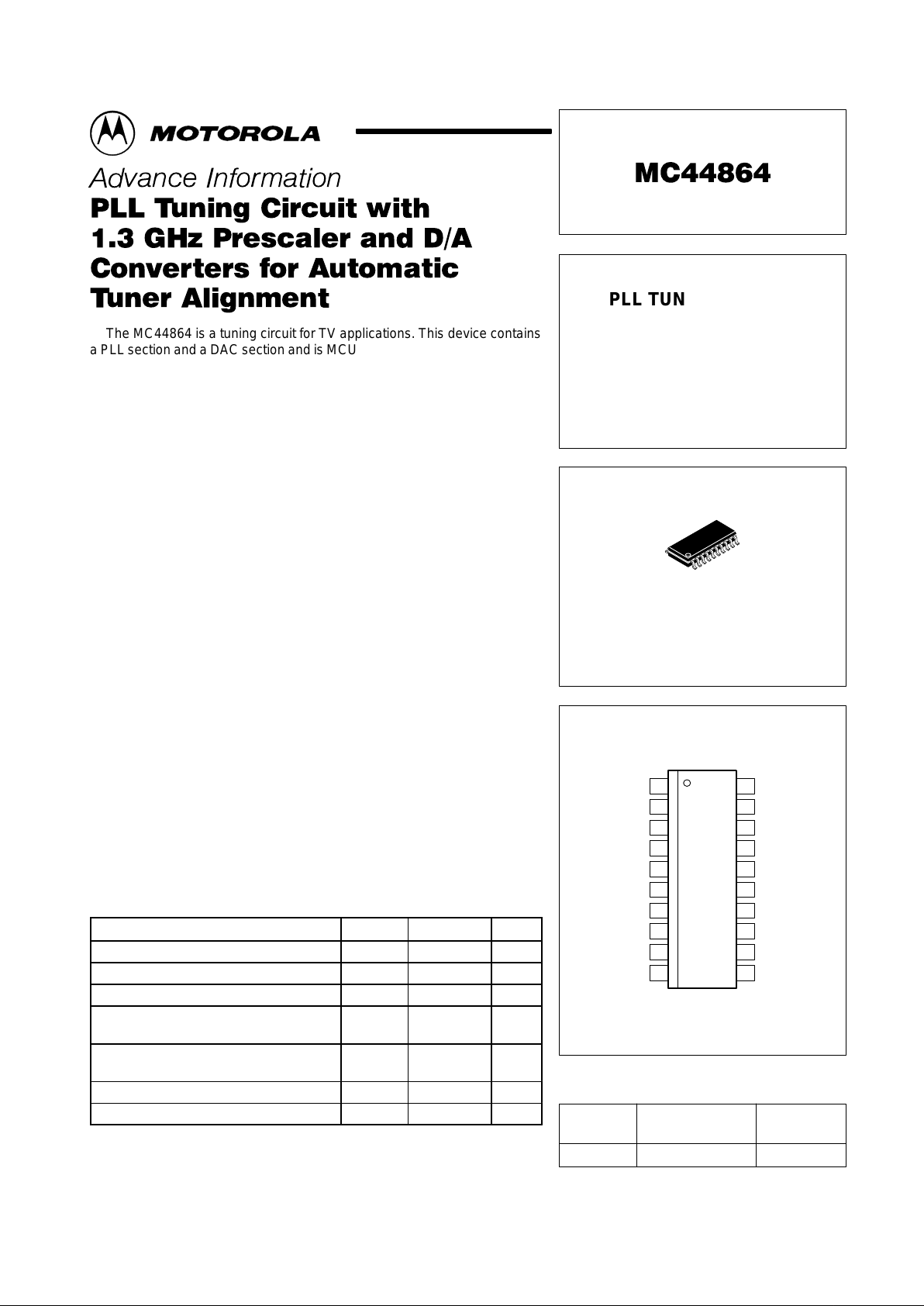
PIN CONNECTIONS
Order this document by MC44864/D
M SUFFIX
PLASTIC PACKAGE
CASE 967
(EIAJ–20)
20
1
8
V
TUN
18
17
16
15
14
13
12
3
4
5
6
7
9
Amp In
V
CC2
DA2
DA3
V
CC1
Gnd
DA1
SCL
B
7
B
5
B
3
B
1
CA
(Top View)
20
19
1
2
XTAL
PHO
Gnd
SDA
1110
HF
1
HF
2
SEMICONDUCTOR
TECHNICAL DATA
Device
Operating
Temperature Range
Package
ORDERING INFORMATION
MC44864M TA = 0° to +70°C EIAJ–20
1
MOTOROLA ANALOG IC DEVICE DATA
! ! #
$
" !
!
The MC44864 is a tuning circuit for TV applications. This device contains
a PLL section and a DAC section and is MCU controlled through an I2C Bus.
The PLL section contains all the functions required to control the VCO of a
TV tuner. The IC generates the tuning voltage and the additional control
signals, such as band switching voltages.
The D/A section generates three additional varactor voltages to feed all of
the varactors of the tuner with individually optimized control voltages
(automatic tuner adjustment). The MC44864 is manufactured on a single
silicon chip using Motorola’s high density bipolar process, MOSIAC
(Motorola Oxide Self–Aligned Implanted Circuits).
• Complete Single Chip System for MPU Control
• Selectable ÷8 Prescaler Accepts Frequencies up to 1.3 GHz
• 15 Bit Programmable Divider Accepts Input Frequencies up to 165 MHz
• Programmable Reference Divider
• 3–State Phase/Frequency Comparator
• Operational Amplifier for Direct V aractor Control with Low Saturation
Voltage
• Four Output Buffers (15 mA)
• Output Options for 62.5 kHz, Reference Frequency and the
Programmable Divider
• The HF Input is Symmetrical
• Three 6 Bit DACs for Automatic Tuner Adjustment Allowing Use of
Non–Matched Varactors
• Better Tuner Performances Through Optimum Filter Response
• I
2
C Bus Controlled
• Four Chip Addresses for the PLL Section
• Four Chip Addresses for the D/A Section
• ESD Protected to MIL–STD–883C, Method 3015.7
(2,000 V, 1.5 kΩ, 150 pF)
MOSAIC is a trademark of Motorola, Inc.
MAXIMUM RATINGS (T
A
= 25°C, unless otherwise noted.)
Rating Pin Value Unit
Power Supply Voltage (V
CC1
) 9 6.0 V
Band Buffer “Off” Voltage 14 – 17 15 V
Band Buffer “On” Current 14 – 17 20 mA
Operational Amplifier Power Supply
Voltage (V
CC2
)
4 36 V
Operational Amplifier Short Circuit Duration
(0 to V
CC2
)
5 – 8 Continuous S
Storage Temperature – –65 to +150 °C
Operating Temperature Range – 0 to +70 °C
NOTE: ESD data available upon request.
Motorola, Inc. 1996 Rev 2
Page 2
MC44864
2
MOTOROLA ANALOG IC DEVICE DATA
Representative Block Diagram
HF
1
HF
2
SCL
SDA
V
CC1
5.0 V
CA
V
CC2
33 V
Amp
In
XTAL
Gnd
Gnd
DA3 DA2 DA1 V
TUN
PHO
18
19
Buffers
Test
Logic
Bias
D/A 3
6 Bit
D/A 2
6 Bit
D/A 1
6 Bit
Ref
Voltage
Decoder
Shift Register
8 Bit
Phase
Comp
Latches
Shift Register
15 Bit
Latches A
Latches B
Program Divider
15 Bit
Latch
Control
I2C Bus
Receiver
÷
8
Presc
Preamp 1
Preamp 2
F
out
Ref
Divider
4.0 MHz
Osc
F1
62.5 kHz
TDI
F
ref
F
out
DTC
DTB
FUN
CL
Data
AD1
AD2 DTF
AVA
10
F
outFref
F1
8
Amp 4 Amp 3 Amp 2
3
9
13
4
12
1
20
765
11
2
Amp 1
Latches Latches Latches Latches
B7B5B3B
1
B7B5B3B
1
17 16 15 14
This device contains 3,551 active transistors.
Page 3
MC44864
3
MOTOROLA ANALOG IC DEVICE DATA
ELECTRICAL CHARACTERISTICS (V
CC1
= 5.0 V , V
CC2
= 32 V, TA = 25°C, unless otherwise noted.)
Characteristic
Pin Min Typ Max Unit
V
CC1
Supply Voltage Range 9 4.5 5.0 5.5 V
V
CC1
Supply Current (V
CC1
= 5.0 V)
(1)(2)
9 – 50 70 mA
V
CC2
Supply Voltage Range 4 25 30 35 V
V
CC2
Supply Current (Output Open) 4 – 1.3 2.5
(4)
mA
Band Buffer Leakage Current when “Off” at 12 V 14 – 17 – 0.01 1.0 µA
Band Buffer Saturation Voltage when “On” at 15 mA 14 – 17 – 1.8 2.0 V
Data/Clock Current at 0 V 18, 19 –10 – 0 µA
Clock Current at 5.0 V 18 0 – 1.0 µA
Data Current at 5.0 V Acknowledge “Off” 19 0 – 1.0 µA
Data Saturation Voltage at 15 mA Acknowledge “On” 19 – 1.2 – V
Data/Clock Input Voltage Low 18, 19 – – 1.5 V
Data/Clock Input Voltage High 18, 19 3.0 – – V
Clock Frequency Range 18 – – 100 kHz
Phase Detector Current in High Impedance State 2 –15 – 15 nA
Oscillator Frequency Range 1, 2 3.5 4.0 4.1 MHz
Phase Detector High–State Source Current (@ 1.5 V) 2 –2.5 – –0.5 mA
Phase Detector Low–State Sink Current (@ 4.0 V) 2 0.5 – 2.5 mA
Operational Amplifier Internal Reference Voltage – 2.0 2.5 3.0 V
Operational Amplifier Input Current 3 –15 – 15 nA
DC Open Loop Gain – 2000 – – V/V
Gain Bandwidth Product – – 0.2 – MHz
Phase Margin – – 50 – Deg.
V
out
Low, Sinking 50 µA 6 – 8 – 0.2 0.5 V
V
out
High, Sourcing 50 µA (V
CC2
– V
out
High) 6 – 8 – – 1.5 V
Tuning V oltage (DC) 5 – 8 – – 30 V
D/A Converters Step Size
(3)
6 – 8 0.5 – 1.5 LSB
D/A Converters Temperature Drift 6 – 8 – 1.0 – LSB
DAC Offset at V
TUN
= 2.5 V – –50 – 50 mV
DAC Offset at V
TUN
= 25 V – –700 – 700 mV
DAC Voltages (DC) 6 – 8 – – 33 V
NOTES: 1. When prescaler “Off”, typical supply current is decreased by 10 mA.
2.Band Buffers “Off”, 2.4 mA more when one buffer is on.
3.For definition of the LSB, see Figure 9 in the D/A section.
4.2.5 mA as long as the analog outputs are not in saturation high, which means V
TUN
, V
DAC
(Pins 5, 6, 7, 8) lower than V
CC2
– 1.5 V. When all
outputs are in saturation high the maximum V
CC2
current is 5.0 mA.
Page 4
MC44864
4
MOTOROLA ANALOG IC DEVICE DATA
HF CHARACTERISTICS (See Figure 1)
Characteristic
Pin Min Typ Max Unit
DC Bias 10, 11 – 1.55 – V
Input Voltage Range mVrms
10–150 MHz (Prescaler “Off”) 10, 1 1 20 – 315
80–1000 MHz 10, 11 20 – 315
1000–1300 MHz 10, 11 50 – 315
50 Ω Cable
Figure 1. HF Sensitivity Test Circuit
MC44864
Device is in test mode: B7 is “On”, R2 = 1 and R3 = 0 (see Bus section).
Sensitivity is the level of the HF generator on 50 Ω load (without MC44864 load).
18, 19
10 12 1
Bus Controller
HF Generator
HF Out Gnd
9
V
CC1
Frequency
Counter
In
I2C Bus
1.0 nF
11
+5.0 V
17
50
Ω
4.0 MHz
22 pF
1.0 nF
3.9 k
B
7
12 V
–j +j
2
0.5
1
0.5
1
2
0.5
1
2
Figure 2. Typical HF Input Impedance
ZO = 50
Ω
500 MHz
1.3 GHz
1.0 GHz
50 MHz
0
Page 5

MC44864
5
MOTOROLA ANALOG IC DEVICE DATA
PIN FUNCTION DESCRIPTION
Pin Symbol Description
6, 7, 8 DA1, DA2, DA3 D/A output control voltages
9 V
CC1
Positive supply of the circuit (except DACs)
10, 11 HF1, HF
2
HF input from local oscillator
12, 20 Gnd Ground
13 CA Chip Address
14, 15, 16, 17 B1, B3, B5, B
7
Band buffer output can drive 15 mA
18 SCL Clock input (supplied by the microprocessor via Bus)
19 SDA Data input (bus)
1 XTAL Crystal oscillator (typically 4.0 MHz)
2 PHO Phase comparator output
3 Amp In Negative operational amplifier input
4 V
CC2
Operational amplifier positive supply
5 V
TUN
Operational amplifier output which provides the tuning voltage
Page 6

MC44864
6
MOTOROLA ANALOG IC DEVICE DATA
Figure 3. Pin Circuit Schematic
DA1
6
DA2
7
DA3
8
V
CC1
9
HF
1
10
HF
2
11
Gnd
12
CA
13
B
1
14
B
3
15
V
CC2
4
Amp
In
3
PHO
2
XTAL
1
Gnd
20
SDA
19
SCL
18
B
7
17
B
5
16
V
TUN
5
Amp
Out
Amp
Out
Amp
Out
20 V
20 V
600 k
20 V
20 V
20 V
20 V
5.5 V
5.5 V
5.5 V
5.5 V
20 V
Buffer
Buffer
Buffer
2.0 k
2.0 k
20 k
V
CC1
1.1 mA 0.4 mA
Buffer
On/Off
V
CC1
5.0 µA
25 k
40 k
20 k
15 k
V
CC1
10 k
V
CC1
150 k
50 k
IB
Comp
10 k
20 V
V
CC1
130 k100 k
50
20 V
100 k
ACK
1.5 k 100
5.5 V
20 V
1.0 k
10 k
5.5 V
20 V
1.0 k
1.0 k
V
CC1
2.5 k
5.5 V
20 V
500
20 V
Page 7

MC44864
7
MOTOROLA ANALOG IC DEVICE DATA
FUNCTIONAL DESCRIPTION
A representative block diagram and a typical system
application are shown in Figures 4 and 5. A discussion of the
features and function of the internal blocks is given below.
Automatic Tuner Alignment
The circuit generates the tuning voltage through the PLL.
The output voltages of the D/A converters are equal to the
tuning voltage plus a positive or negative offset of up to 31
steps. During the automatic alignment one first lets the PLL
lock to the appropriate frequency and then searches for the
optimum value of the other varactor voltages. The digital
word for each voltage value is stored in a nonvolatile memory
(NVM). Hence, for each frequency point to be adjusted, three
times 6 bits of information have to be stored (plus 2 bits for
the DAC range).
The information stored in the NVM reflects the
characteristic of the individual tuner. For this reason, the
NVM is preferably situated inside the tuner and is also
controlled by the I2C Bus.
5
Figure 4. Block Diagram
HF
1
HF
2
SCL
SDA
V
CC1
5.0 V
CA
V
CC2
33 V
Amp
In
XTAL
Gnd
Gnd
DA3 DA2 DA1 V
TUN
PHO
18
19
Buffers
Test
Logic
Bias
D/A 3
6 Bit
D/A 2
6 Bit
D/A 1
6 Bit
Ref
Voltage
Decoder
Shift Register
8 Bit
Phase
Comp
Latches
Shift Register
15 Bit
Latches A
Latches B
Program Divider
15 Bit
Latch
Control
I2C Bus
Receiver
÷
8
Presc
Preamp 1
Preamp 2
F
out
Ref
Divider
4.0 MHz
Osc
F1
62.5 kHz
TDI
F
ref
F
out
DTC
DTB
FUN
CL
Data
AD1
AD2 DTF
AVA
10
F
outFref
F1
8
Amp 4 Amp 3 Amp 2
3
9
13
4
12
1
20
76
11
2
Amp 1
Latches Latches Latches Latches
B7B5B3B
1
Bands and
Controls Out
17 16 15 14
10 k
15 k
1.0 n 1.0 n 1.0 n
1.0 n
180 n
39 n
18 k
(1)
1.0 n
10 k
10 k
(2)
NOTES: 1. Pin 13: Short to V
CC
for addresses CC, CE
Resistors ±10% for addresses C8, CA (values 10 k and 15 k) for test only
Open or 1.0 nF to Gnd for addresses C4, C6
Short to Gnd for addresses C0, C2
2.The crystal may be connected to Pin 20 with no connection to external Gnd.
Page 8

MC44864
8
MOTOROLA ANALOG IC DEVICE DATA
Figure 5. TV Tuner for Automatic Alignment
VHFUHF
12 V
AGC
DA1
Mixer
Filter
Filter
Local
Oscillator
IF
33 V
5.0 V
SCL
MC44864
PLL–D/A IC
Band Buffers
BIII
SDA
DA2DA3
V
CC3
Antenna
HF Input
XTAL
V
CC2
V
CC1
Clock
Data
D–to–A
Converters
NVM
Phase CmpAmp InV
TUN
Figure 6. Definition of Bytes
CA1_PLL Chip Address 1 1 0 0 A
3
A
2
A
1
A0 = 0 ACK
CO_Control Information 1 R
6
T P R
3
R
2
R
1
R
0
ACK
BA_Band Information B
7
X B
5
X B
3
X B
1
X ACK
FM_Frequency Information (with MSB) 0 N
14
N
13
N
12
N
11
N
10
N
9
N
8
ACK
FL_Frequency Information (with LSB) N
7
N
6
N
5
N
4
N
3
N
2
N
1
N
0
ACK
Chip Addresses
The chip address is programmable by Pin CA.
The PLL addresses C0, C2, C4, C6 are officially allocated
to PLL–IC’s.
The addresses C8, CA, CC, CE are not officially allocated.
Care has to be taken in the application that no conflict occurs
with other devices on the same I2C Bus when using the
addresses C8 to CE.
CA Pin (13) A3A2A1A0Address Function
–0.04 V
CC1
to
0.1 V
CC1
0000010
0
C0
C2
1st PLL
1st DAC
Open or 0.2
V
CC1
to 0.3 V
CC1
0011010
0
C4
C6
2nd PLL
2nd DAC
0.42 V
CC1
to
0.75 V
CC1
1100010
0
C8
CA
3rd PLL
3rd DAC
0.9 V
CC1
to 1.2
V
CC1
1111010
0
CC
CE
4th PLL
4th DAC
PLL SECTION
Data Format and Bus Receiver
The circuit receives the information for tuning and control
via I2C Bus. The incoming information is treated in the bus
receiver. The definition of the permissible bus protocol is
shown in the four examples below:
Ex. 1 STA CA1 CO BA STO
Ex. 2 STA CA1 FM FL STO
Ex. 3 STA CA1 CO BA FM FL STO
Ex. 4 STA CA1 FM FL CO BA STO
STA = Start Condition
STO = Stop Condition
CA1 = Chip Address Byte of the PLL Section
CO = Data Byte for Control Information
BA = Band Information
FM = Data Byte for Frequency Information (MSB’s)
FL = Data Byte for Frequency Information (LSB’s)
Figure 6 shows the five bytes of information that are
needed for circuit operation: there is a chip address, two
bytes of control and band information and two bytes of
frequency information.
Page 9

MC44864
9
MOTOROLA ANALOG IC DEVICE DATA
After the chip address, two or four data bytes may be
received: if three data bytes are received, the third data byte
is ignored. If five or more data bytes are received, the fifth
and following data bytes are ignored and the last
acknowledge pulse is sent at the end of the fourth data byte.
The first and the third data bytes contain a function bit F. If
the function bit F= 0, frequency information is acknowledged
and if F = 1, control/band information is acknowledged.
If the address is correct (signal AD1) the information is
loaded into latches.
A function bit in the first and third data byte is used to pass
this data either into the latches of the programmable divider
(signal DTF) or into the latches for band and control information
(signal DTB). The data transfer to the latches (signals DTF and
DTB) is initiated after the 2nd and 4th data bytes.
A second string of latches is used for the data transfer into
the programmable divider to inhibit the transfer during the
preset operation (signal TDI, signal AVA is an internal
“address valid” command).
The switching levels of clock and data (Pins 18 and 19) are
0.5 x V
CC1
.
The control and band information bits have the following
functions.
Bits R0, R1: Controls Reference Divider Division Ratio
R
0
R
1
Division Ratio
0
1
0
1
0
0
1
1
2048
1024
512
256
Bits R2, R3: Switches Internal Signals to the Buffer
Outputs
R
2
R
3 Pin 16
Pin 17
0
0
1
1
0
1
0
1
–
62.5 kHz
F
ref
–
–
–
F
BY2
–
Bit B5 has to be “one” when Pin 16 is used to output 62.5
kHz. Bits B5 and B7 have to be “one” to output F
ref
and F
BY2
.
F
BY2
is the programmable divider output frequency divided
by two.
Bits R2, R6, T: Controls the Phase Comparator Output
Stage
R
2
R
6
T Output State
0
0
0
0
1
1
1
1
0
0
1
1
0
0
1
1
0
1
0
1
0
1
0
1
Normal Operation
“Off” (High Impedance)
High
Low
Normal Operation
“Off”
Normal Operation
“Off”
The Band Buffers
The band buffers are open collector transistors and are
active “low” at Bn = 1. They are designed for 15 mA with
typical on–voltage of 1.8 V. These buffers are designed to
withstand relative high output voltage in the off–state (15 V).
B5 and B7 buffers (Pins 16 and 17) may also be used to
output internal IC signals (reference frequency and
programmable divider output frequency divided by 2) for test
purposes.
Buffer B5 may also be used to output a 62.5 kHz frequency
from an intermediate stage of the reference divider. The bits
B5 and B7 have to be “one” if the buffers are used for these
additional functions.
The Programmable Divider
The programmable divider is a presettable down counter.
When it has counted to zero it takes its required division ratio
out of the latches B. Latches B are loaded from latches A by
means of signal TDI which is synchronous to the
programmable divider output signal.
Since latches A receive the data asynchronously with the
programmable divider, this double latch scheme is needed to
assure correct data transfer to the counter.
The division ratio definition is given by:
N = 16384 x N14 + 8192 x N13 + … + 4 x N2 + 2 x N1 + N
0
Maximum Ratio 32767
Minimum Ratio 256
where N0 … N14 are the different bits for frequency
information.
The counter reloads correctly as long as its output
frequency does not exceed 1.0 MHz.
Division ratios of < 256 are not allowed. At power–up the
counter bit N8 is preset to “1”. All other bits are undetermined.
In this way, the counter always starts with a division ratio of
256 or higher.
The data transfer between latches A and B (signal TDI) is
also initiated by any start condition on the bus.
At power–on the whole bus receiver is reset and the
programmable divider is set to a counting ratio of N = 256 or
higher.
The Prescaler
The prescaler has a preamplifier and may be bypassed
(Bit P). The signal then passes through preamplifier 2.
The table on the following page shows the frequency
ranges which may be synthesized with and without prescaler .
The Phase Comparator
The phase comparator is phase and frequency sensitive
and has very low output leakage current in the high
impedance state.
The Operational Amplifier
The operational amplifier for the tuning voltage is designed
for low noise, low input bias current and high power supply
rejection. The positive input is biased internally. The
operational amplifier needs 30 V supply (V
CC2
) as minimum
voltage for a guaranteed maximum tuning voltage of 28.5 V.
Figure 4 shows the usual filter arrangement. The
component values depend very much on the application
(tuner characteristic, reference frequency, etc.).
As a starting point for optimization, the component values
in Figure 4 may be used for 7.8125 kHz reference frequency
in a multiband TV tuner.
The Oscillator
The oscillator uses a 4.0 MHz crystal tied to ground in
series with a capacitor. The crystal operates in the series
resonance mode.
The crystal is driven through a 1.6 kΩ resistor on chip.
The voltage at Pin 16 “crystal”, has low amplitude and low
harmonic distortion.
The negative resistance of the oscillator at Pin 1 (XTAL) is
about 3.0 kΩ.
Page 10

MC44864
10
MOTOROLA ANALOG IC DEVICE DATA
With Int. Prescaler
P = 0
Without Prescaler
P = 1
I
nput Data
R
0
R
1
Ref. Divider
Div. Ratio
Ref. Freq.
Hz
(1)
Frequency
Steps kHz
Max. Input
Freq. MHz
Frequency
Steps kHz
Max. Imput
Freq. MHz
0
1
0
1
0
0
1
1
2048
1024
512
256
1953.125
3906.25
7812.5
15625.0
15.625
31.25
62.5
125.0
512
1024
1300
(2)
1300
(2)
1.953125
3.90625
7.8125
15.625
64
128
165
(3)
165
(3)
NOTES: 1. With 4.0 MHz Crystal
2.Limit of Prescaler
3.Limit of Programmable Divider
For satellite tuner applications the circuit may be used with an external /4 prescaler and a reference divider ration of 1024 (R0 = 1, R1 = 0). In this way,
frequencies up to 4.0 GHz can be synthesized with 125 kHz resolution (4.0 MHz crystal).
The same result can be achieved with an external /32 prescaler when the internal prescaler is bypassed (P = 1).
The Reference Divider
The reference divider of the MC44864 is programmable
(Bits R0 and R1) for ratios of 2048, 1024, 512 and 256. This
feature makes the circuit versatile.
Bit P: Controls the Prescaler
P Prescaler Function
0
1
Prescaler Active
Prescaler Bypassed
Prescaler Power Supply “Off”
Bits B1, B3, B5, B7: Controls the Band Buffers
B1, B3, B5, B7 = 0
B0, B1, B, B73 = 1
Buffer “Off”
Buffer “On”
D/A SECTION
Basic Function
The D/A section has four separate chip addresses from
the PLL section. Three D–to–A converters that have a
resolution of 6 bits (5 bits plus sign) are on chip. The analog
output voltages are dc. The converters are buffered to the
analog outputs DA1, DA2 and DA3 by operational amplifiers
with an output voltage range that is equal to the tuning
voltage range (about 0 to 30 V). The operational amplifiers
are arranged such that a positive or negative offset can be
generated from the tuning voltage.
Data Format and Bus Protocols
The D–to–A information consists of the D/A chip address
(CA2) and four data bytes. The first two bits of the data bytes
are used as the function address. Thus the bytes C1, C2 and
C3 contain the address for the individual converter and the 6
bits to be converted. Bit D5 is the sign (log “1” for positive
offset, log “0” for negative offset) and the bits D0 to D
4
determine the number of steps to be made as an offset from
the tuning voltage. The bits S0 and S1 in the data byte RA
define the step size (V
step
) and the range of the converters
(see Figures 8 and 9). The range is the same for all
converters.
After the chip address (CA2) is acknowledged, up to four
data bytes may be received by the IC. If more than four bytes
are received, the fifth and following bytes are ignored and the
last acknowledge pulse is sent after the fourth data byte. The
data transfer to the converters (signal DTC) is initiated each
time a complete data byte is received.
The following shows some examples of the permissible
bus protocols of the D–to–A section. The data bytes may be
sent to the IC in random order with up to four in one
sequence. The same converter may be loaded up to four
times as shown in example 6. Below are 6 examples of
permissible bus protocols.
Ex. 1 STA CA2 C1 STO
Ex. 2 STA CA2 C1 C2 STO
Ex. 3 STA CA2 C1 C2 C3 STO
Ex. 4 STA CA2 C1 C2 C3 RA STO
Ex. 5 STA CA2 RA C1 C2 C3 STO
Ex. 6 STA CA2 C1 C1 C1 C1 STO
STA = Start Condition
STO = Stop Condition
CA2 = Chip Address Byte for D/A Section
C1, C2, C3 = Data Bytes for D/A Converters
RA = Data Byte for Range
Figure 7. Definition of Bytes
CA2_D/A Chip Address 1 1 0 0 A
2
A
1
A0 = 0 ACK
C1_Converter 1 0 0 D
5
D
4
D
3
D
2
D
1
D
0
ACK
C2_Converter 2 0 1 D
5
D
4
D
3
D
2
D
1
D
0
ACK
C3_Converter 3 1 0 D
5
D
4
D
3
D
2
D
1
D
0
ACK
RA_Range Selection 1 1 X X X X S
1
S
0
ACK
Page 11

MC44864
11
MOTOROLA ANALOG IC DEVICE DATA
Figure 8. Output Voltage (D/A Converters)
VDA = V
TUN
± V
step
(D0 +2 D1 +4 D2 +8 D3 + 16 D4)
D5 = 1 positive sign; D5 = 0 negative sign
V
TUN
: Tuning Voltage set by PLL
V
step
: Voltage Step (LSB) of the D/A Converters
Figure 9. Range Selection of the D/A Converters
Input Data
Guaranteed
S
0
S
1
Typ. Step Size
V
step
R
ange
31
Steps
0
1
0
1
0
0
1
1
225 mV
125 mV
70 mV
40 mV
6.25 V
3.40 V
1.90 V
1.05 V
The D/A Converters
The D/A converters convert 5 bit into analog current of
which the polarity is switched by the sixth bit. The reference
voltage of the converters is programmed by two bits (S0, S
1
of the RA–byte) to determine the scaling factor. The analog
currents are then converted into voltages and added to their
respective operational amplifier nominal bias. The resulting
voltages at Pins 6, 7 and 8 are the tuning voltages (V
TUN
, see
Figure 4) at Pin 5 plus any offset provided by information in
the D/A converters.
If the data bits D0 to D4 are all “0”, the three D/A output
voltages on Pins 6, 7 and 8 are equal to the tuning voltage
(Pin 5) within the DAC offset voltages.
The four amplifiers have the same output characteristics
with the maximum output voltage being 1.5 V lower than
V
CC2
in the worst case. The four analog outputs are
short–circuit protected. At power–up, the D/A outputs are
undetermined.
The D/A converters are guaranteed to be monotonic with a
voltage step variation of ±0.5 LSB.
The D/A converters work correctly as long as the PLL loop
is active. V
TUN
is then between 0.3 V and V
CC2
– 1.5 V . If the
loop saturates, the DACs do not work.
The DAC–OFFSET is defined as the difference between
the DAC output voltage (with bits D0 to D4 = 0) and the tuning
voltage (PLL active). The DAC operation is guaranteed from
0.3 V to V
CC2
– 1.5 V. On typical samples, the DACs will
operate down to 0.2 V.
DAC Offset
(V
DAC
– V
TUN
)
V
TUN
10 20 30 V
±
700 mVmax
±
50 mVmax
Figure 10. Definition of DAC Offset
Page 12

MC44864
12
MOTOROLA ANALOG IC DEVICE DATA
M SUFFIX
PLASTIC PACKAGE
CASE 967–01
(EIAJ–20)
ISSUE O
OUTLINE DIMENSIONS
DIM MIN MAX MIN MAX
INCHES
––– 2.05 ––– 0.081
MILLIMETERS
0.05 0.20 0.002 0.008
0.35 0.50 0.014 0.020
0.18 0.27 0.007 0.011
12.35 12.80 0.486 0.504
5.10 5.45 0.201 0.215
1.27 BSC 0.050 BSC
7.40 8.20 0.291 0.323
0.50 0.85 0.020 0.033
1.10 1.50 0.043 0.059
0
0.70 0.90 0.028 0.035
––– 0.81 ––– 0.032
A
1
H
E
Q
1
L
E
_
10
_
0
_
10
_
NOTES:
1 DIMENSIONING AND TOLERANCING PER ANSI
Y14.5M, 1982.
2 CONTROLLING DIMENSION: MILLIMETER.
3 DIMENSIONS D AND E DO NOT INCLUDE MOLD
FLASH OR PROTRUSIONS AND ARE MEASURED
AT THE PARTING LINE. MOLD FLASH OR
PROTRUSIONS SHALL NOT EXCEED 0.15 (0.006)
PER SIDE.
4 TERMINAL NUMBERS ARE SHOWN FOR
REFERENCE ONLY.
5 THE LEAD WIDTH DIMENSION (b) DOES NOT
INCLUDE DAMBAR PROTRUSION. ALLOWABLE
DAMBAR PROTRUSION SHALL BE 0.08 (0.003)
TOTAL IN EXCESS OF THE LEAD WIDTH
DIMENSION AT MAXIMUM MA TERIAL CONDITION.
DAMBAR CANNOT BE LOCATED ON THE LOWER
RADIUS OR THE FOOT. MINIMUM SPACE
BETWEEN PROTRUSIONS AND ADJACENT LEAD
TO BE 0.46 ( 0.018).
H
E
A
1
L
E
Q
1
_
c
A
Z
D
E
20
110
11
b
M
0.13 (0.005)
e
0.10 (0.004)
VIEW P
DETAIL P
M
L
A
b
c
D
E
e
L
M
Z
Motorola reserves the right to make changes without further notice to any products herein. Motorola makes no warranty , representation or guarantee regarding
the suitability of its products for any particular purpose, nor does Motorola assume any liability arising out of the application or use of any product or circuit, and
specifically disclaims any and all liability, including without limitation consequential or incidental damages. “T ypical” parameters which may be provided in Motorola
data sheets and/or specifications can and do vary in different applications and actual performance may vary over time. All operating parameters, including “Typicals”
must be validated for each customer application by customer’s technical experts. Motorola does not convey any license under its patent rights nor the rights of
others. Motorola products are not designed, intended, or authorized for use as components in systems intended for surgical implant into the body, or other
applications intended to support or sustain life, or for any other application in which the failure of the Motorola product could create a situation where personal injury
or death may occur. Should Buyer purchase or use Motorola products for any such unintended or unauthorized application, Buyer shall indemnify and hold Motorola
and its officers, employees, subsidiaries, affiliates, and distributors harmless against all claims, costs, damages, and expenses, and reasonable attorney fees
arising out of, directly or indirectly, any claim of personal injury or death associated with such unintended or unauthorized use, even if such claim alleges that
Motorola was negligent regarding the design or manufacture of the part. Motorola and are registered trademarks of Motorola, Inc. Motorola, Inc. is an Equal
Opportunity/Affirmative Action Employer.
How to reach us:
USA/EUROPE/Locations Not Listed: Motorola Literature Distribution; JAPAN: Nippon Motorola Ltd.; Tatsumi–SPD–JLDC, 6F Seibu–Butsuryu–Center,
P.O. Box 20912; Phoenix, Arizona 85036. 1–800–441–2447 or 602–303–5454 3–14–2 Tatsumi Koto–Ku, Tokyo 135, Japan. 03–81–3521–8315
MFAX: RMF AX0@email.sps.mot.com – TOUCHT ONE 602–244–6609 ASIA/P ACIFIC: Motorola Semiconductors H.K. Ltd.; 8B Tai Ping Industrial Park,
INTERNET: http://Design–NET.com 51 Ting Ko k Road, Tai Po, N.T., Hong Kong. 852–26629298
MC44864/D
*MC44864/D*
◊
 Loading...