

Page 1
SEMICONDUCTOR
TECHNICAL DATA
LOW–POWER
PLL TUNING CIRCUIT
PIN CONNECTIONS
Order this document by MC44827/D
116
15
14
13
12
11
10
9
2
3
4
5
6
7
8
DA
CL
XTAL
V
CC2
33 V
V
CC1
5.0 V
HF In
EN
Gnd
DTB SUFFIX
PLASTIC PACKAGE
CASE 948F
(TSSOP–16)
16
1
Amp In
V
TUN
Lock
V
CC3
12 V
B3
B2
B1
B0
(Top View)
FOR 3–WIRE BUS WITH
1.3 GHz PRESCALER
1
MOTOROLA ANALOG IC DEVICE DATA
The MC44827/27B are tuning circuits for TV and VCR tuner applications.
They contain on one chip all the functions required for PLL control of a VCO.
The integrated circuits also contain a high frequency prescaler and thus can
handle frequencies up to 1.3 GHz.
The MC44827 has programmable 512/1024 reference divider while the
MC44827B has a fixed reference divider of 1024.
The MC44827/27B offer the same features as MC44817/17B but has
improved sensitivity performance and reduced power dissipation. The low
frequency preamplifier has been removed and the operational amplifier
pull–up resistor has been increased to 60 kΩ.
The MC44827/27B are controlled via a 3–wire bus. The MC44827/27B
have the same functions as the MC44828 which is I2C bus controlled. The
MC44827/27B and the MC44828 can be exchanged to allow conversion
between 3–wire bus and I2C bus control.
The MC44827/27B are manufactured on a single silicon chip using
Motorola’s high density bipolar process, MOSAIC (Motorola Oxide Self
Aligned Implanted Circuits).
• Complete Single Chip System for MPU Control (3–Wire Bus). Data and
Clock Inputs are I2C Bus Compatible
• Divide–by–8 Prescaler Accepts Frequencies up to 1.3 GHz
• 15 Bit Programmable Divider Accepts Input Frequencies up to 165 MHz
• 3–State Phase/Frequency Comparator
• Operational Amplifier for Direct Tuning Voltage Output (30 V)
• Four Integrated PNP Band Buffers can drive up to 40 mA
(V
CC1
to 14.4 V)
• Output Options for the Reference Frequency and the
Programmable Divider
• Bus Protocol for 18 or 19 Bit Transmission
• Extra 34–Bit Protocol for Test and Further Features
• High Sensitivity Preamplifier
• Lower Power Consumption, 200 mW Typical
• Improved Prescaler with Higher Margins for Sensitivity and
Temperature Range
• Lock Detector with Push–Pull Output
• Space–Saving TSSOP Package
• ESD Protected to MIL–STD–883C, Method 3015.7 (1.5 kΩ,100 pF)
MOSAIC is a trademark of Motorola, Inc.
ORDERING INFORMATION
Device
Operating
Temperature Range
Package
MC44827DTB
°
°
MC44827BDTB
T
A
= –
20° t
o +
80°C
TSSOP–16
Motorola, Inc. 1998 Rev 1
Page 2
MC44827/27B
2
MOTOROLA ANALOG IC DEVICE DATA
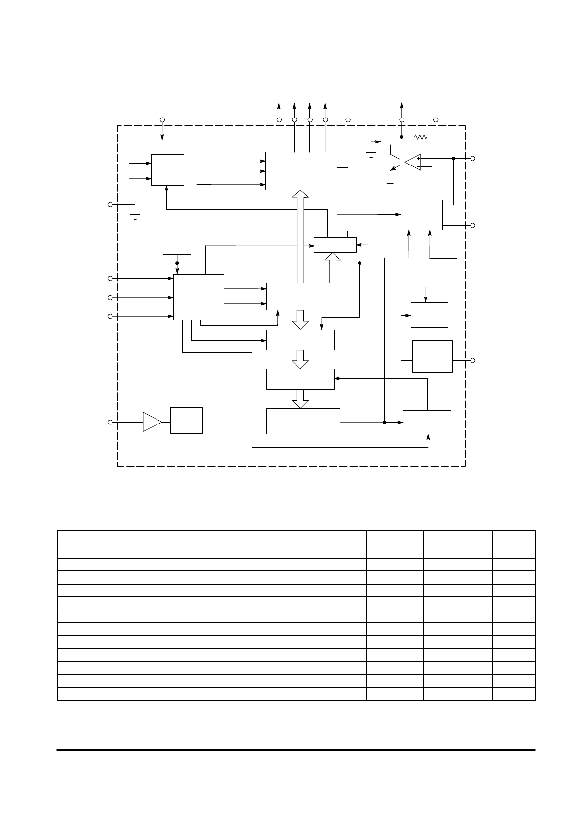
Figure 1. Representative Block Diagram
This device contains 3,204 active transistors.
Gnd
Test
Logic
Buffers
Latches
P–On
Reset
3–Wire Bus
Receiver
Latches
Phase
Comp
Ref
Divider
Osc
Latch Control
Program Divider
15 Bit
Latches B
Latches A
÷
8
Prescaler
Preamp 1
DTB2
POR
Operational
Amplifier
V
ref
60 k (1)
DTB1
CL
Data
RL
DTF
F
out
TDI
F
out
F
ref
T5
T0
…
T2
T4
4
6
15
10111213 14 5 675.0 V
F
out
F
ref
9
16
1
2
8
EN
DA
CL
HF In
V
CC1
V
CC3
12 V
V
TUN
V
CC2 33 V
Amp In
Lock
XTAL
B3 B2 B1 B0
DTS, EN
512/1024
B = 1024 Only
4
15
3
12 V
NOTE: 1. This part may be used with an external pull–up resistor of 20 kΩ to remain compatible with MC44817/17B
designed tuners. Pin 6 is left open. The internal pull–up can also be used with an external resistor in parallel.
Shift Register
15 Bit
MAXIMUM RATINGS (T
A
= 25°C, unless otherwise noted.)
Rating
Pin Value Unit
Power Supply Voltage (V
CC1
) 7 6.0 V
Band Buffer “Off” Voltage 10–13 14.4 V
Band Buffer “On” Current 10–13 50 mA
Band Buffer Pin Shorted to Ground or V
CC3
(Short Circuit Duration) (Note 1) 10–13 Continuous –
Operational Amplifier Power Supply Voltage (V
CC2
) 6 40 V
Operational Amplifier Pin Shorted to Ground or V
CC2
(Short Circuit Duration) 5 Continuous –
Power Supply Voltage (V
CC3
) 14 14.4 V
Storage Temperature – –65 to +150 °C
Operating Temperature Range – –20 to +80 °C
Band Buffer Operation (Note 2) at 50 mA each Buffer All Buffers “On” Simultaneously 10–13 10 s
Operational Amplifier Output Voltage 5 V
CC2
V
RF Input Level (80 MHz to 1.3 GHz) 8 1.5 Vrms
NOTES: 1. At V
CC3
= V
CC1
to 14.4 V and TA = –20° to +80°C one buffer “On” only.
2.At V
CC3
= V
CC1
to 14.4 V and TA = –20° to +80°C.
3.ESD data available upon request.
Page 3
MC44827/27B
3
MOTOROLA ANALOG IC DEVICE DATA
ELECTRICAL CHARACTERISTICS (Parameter Type: A–100% Tested, B–100% Correlation Tested, C–Characterized on Samples,
D–Design Parameter. V
CC1
= 5.0 V; V
CC2
= 33 V; V
CC3
= 12 V; TA = 25°C, unless otherwise noted.)
Characteristic
Pin Min Typ Max Unit Type
V
CC1
Supply Voltage Range 7 4.5 5.0 5.5 V A
V
CC2
Supply Voltage Range 6 25 32 37 V A
V
CC3
Supply Voltage Range 14 V
CC1
12 14.4 V A
V
CC1
Supply Current (V
CC1
= 5.0 V; V
CC3
= 12 V) One Buffer “On” 7 – 23 30 mA A
V
CC2
Supply Current (Output Open) V
TUN
= 15 V 6 – 0.3 1.0 mA A
V
CC3
Supply Current 14 mA A
All Buffers “Off” – 0.15 0.3
One Buffer “On” when Open – 6.5 8.0
One Buffer “On” at 40 mA – 46.5 50
Band Buffer Leakage Current when “Off” at 12 V 10–13 – 0.01 1.0 µA A
Band Buffer Saturation Voltage when “On” at 30 mA 10–13 – 0.15 0.3 V B
Band Buffer Saturation Voltage when “On” at 40 mA 10–13 – 0.2 0.5 V A
Data/Clock/Enable Current at 0 V 1, 2, 16 –10 – 0 µA A
Data/Clock/Enable Current at 5.0 V 1, 2, 16 0 – 1.0 µA A
Data/Clock/Enable Input Voltage Low 1, 2, 16 – – 1.5 V A
Data/Clock/Enable Input Voltage High 1, 2, 16 3.0 – – V A
Clock Frequency Range 2 – – 100 kHz D
Oscillator Frequency Range 3 3.15 3.2 4.05 MHz D
Operational Amplifier Internal Reference Voltage – 1.8 2.75 3.5 V A
Operational Amplifier Input Current 4 –15 0 15 nA A
DC Open Loop Gain – 100 250 – – B
Gain Bandwidth Product (CL = 1.0 nF) – 0.3 – – MHz C
V
out
Low, Sinking 50 µA (Note 1) 5 – 80 200 mV A
V
out
High, Sourcing 3.0 µA, V
CC2
– V
out
5 – 0.2 0.5 V B
Phase Comparator 3–State Current 4 –15 0 15 nA A
Charge Pump High Current of Phase Comparator 4 30 50 85 µA A
Charge Pump Low Current of Phase Comparator 4 10 15 30 µA A
NOTE: 1. Using the internal 60 kΩ pull–up resistor only.
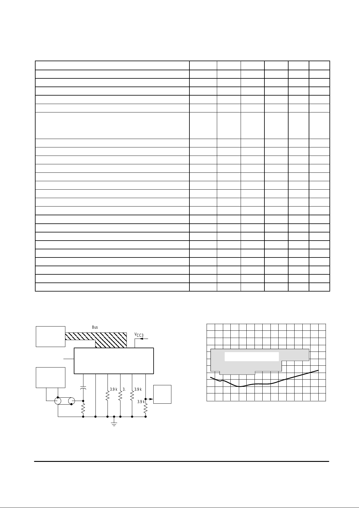
Figure 2. HF (Prescaler Input) Sensitivity Test Circuit
NOTES: 1.Device is in test mode. B2, B3 are “On” and B0, B1 are “Off”.
2.Sensitivity is level of HF generator on 50 Ω load.
16 1 2 14
HF8Gnd9B010B111B212B3
13
Bus Controller
HF Generator
HF Out Gnd
7V
CC1
Counter
In
V
CC3
Bus
3.9 k
3.9 k3.9 k 3.9 k
50
Ω
50 Ω Cable
1.0 nF
MC44827/27B
Guaranteed Operating Area
0
40
RF Level (dBm)
RF In (MHz)
200 400
600
800 1000 1200 1400
20
0
–20
–40
–60
Figure 3. Typical Prescaler Input Sensitivity
Page 4

MC44827/27B
4
MOTOROLA ANALOG IC DEVICE DATA
HF INPUT SENSITIVITY AND OVERLOAD CHARACTERISTICS (V
CC1
= 5.0 V , TA = 25°C.) (See Figure 2.)
Frequency Range
Pin Min Typ Max Unit Type
DC Bias 8 – 1.6 – V A
80–150 MHz 8 10 – 315 mVrms C
150–600 MHz 8 5.0 – 315 mVrms C
600–950 MHz 8 10 – 315 mVrms C
950–1300 MHz 8 50 – 315 mVrms C
Figure 4. Pin Circuit Schematic
500
132 k
V
CC1
96 k
96 k
1/2 V
CC1
V
CC1
96 k
96 k
1/2 V
CC1
20 V
500
132 k
20 V
V
CC1
96 k
96 k
1/2 V
CC1
132 k
500
20 V
5.0 V
100
2.0 k 10 k
20 V
20 V
20 V
100
60 k
20 V
20 V
5.0 V
5.0 V
18 k
2.0 k
2.0 k
1.2
…
1.8 V
“On”/“Off”
“On”/“Off”
“On”/“Off”
“On”/“Off”
2.0 k
20 V
20 V
20 V
20 V
20 V
20 V
16 EN
Enable input
(3–wire bus)
15 Lock
Lock detector output
14 V
CC3
Positive supply for integrated
band buffers (12 V)
13 B3
12 B2
11 B1
10 B0
9 Gnd
Circuit Ground
DA 1
Data input
(3–wire bus)
CL 2
Clock input (supplied
by a microprocessor
via 3–wire bus)
XTAL 3
Crystal oscillator
(3.2 MHz or 4.0 MHz)
AMP In 4
Negative input of
operation amplifier and
phase comparator output
V
TUN
5
Operational amplifier
output which provides
the tuning voltage
V
CC2
6
Operational amplifier
positive supply (33 V)
V
CC1
7
Positive supply of
the circuit (5.0 V)
HF In 8
Input to
prescaler
V
CC1
100 k
Band buffer outputs
can drive up to 30 mA
(40 mA at 0° to 80°C)
20 V
5.0 k
Page 5

MC44827/27B
5
MOTOROLA ANALOG IC DEVICE DATA
PIN FUNCTION DESCRIPTION
Pin Symbol Description
1 DA 3–wire bus data input
2 CL 3–wire bus clock input
3 XTAL Crystal oscillator (3.2 MHz or 4 MHz)
4 Amp In Negative operational amplifier input and phase comparator output
5 V
TUN
Operational amplifier output which provides the tuning voltage
6 V
CC2
Operational amplifier positive supply (33 V)
7 V
CC1
Positive supply of the circuit (5 V)
8 HF In Asymmetrical HF input
9 Gnd Ground
10,11,12,13 B0 to B
3
PNP Band buffer outputs
14 V
CC3
Positive supply for integrated band buffers (12 V)
15 Lock Lock detector output
16 EN 3–wire bus enable input
Data Format and Bus Receiver
The circuit is controlled by a 3–wire bus via Data (DA),
Clock (CL), and Enable (EN) inputs. The Data and Clock
inputs may be shared with other inputs on the I2C–Bus while
the Enable is a separate signal. The circuit is compatible with
18 and 19 bit data transmission and also has a mode for
34 bit transmission for test and additional features.
The 3–wire bus receiver receives data for the internal shift
register after the positive going edge of the EN–signal. The
data is transmitted to the band buffers on the negative going
edge of the clock pulse 4 (signal DTB1).
18 and 19 Bit Data Transmission
The programmable divider may receive a division ratio
coded by a 14 bit (18 bit transmission) or 15 bit (19 bit
transmission). The data is transmitted to the programmable
divider (latches A) on the negative going edge of clock pulse
19 or on the negative edge of the EN–signal if EN goes down
after the 18th clock pulse (signal DTF). If the programmable
divider receives a 14 bit byte, its MSB (bit N14) is internally
reset. The reset pulse is generated only if EN goes negative
after the 18th clock pulse (signal RL).
34 Bit Data Transmission
(For Test and Additional Features)
In the test mode, the programmable divider receives a 15
bit byte and the data is transferred to latches A on the
negative edge of clock pulse 19 (signal DTF). The
information for test is received on clock pulses 20 to 26 and
transmitted to the latches on the negative edge of pulse 34
(signal DTB2). These latches have a power–on reset. The
power–on reset sets the programmable divider to a counting
ratio of 256 or higher and resets the corresponding latches to
the test bits T0 to T6 (signal POR). The bus receiver is not
disturbed if the data format is wrong. Unused bits are
ignored. If for example the Enable signal goes low after clock
pulse 9, bits one to four are accepted as valid buffer
information and the other bits are ignored. If more than 34
bits are received, bit 35 and the following are ignored.
19
27 33195
Standard Bus Protocol 18 or 19 Bit
Bus Protocol for Test and Features
Enable
B3
Buffers Counting Ratio Test & Features Not Used
Buffers Counting Ratio
Clock
Data
26 344201
B2 B1 B0 N14 N13 N12 N1 1 N10 N9 N8 N7 N6 N5 N4 N3 N2 N1 N0 T6 T5 T4 T3 T2 T1 T0 X7 X6 X5 X4 X3 X2 X1 X0
51814
Figure 5. Bus Timing Diagram
Page 6

MC44827/27B
6
MOTOROLA ANALOG IC DEVICE DATA
Definition of Permissible Bus Protocols
1. Bus Protocol for 18 Bit
B3 B2 B1 B0 N13 N12 N11 N10 N9 N8 N7 N6 N5 N4 N3
N2 N1 N0
Max Counting Ratio 16363
N14 is Reset Internally
2. Bus Protocol for 19 Bit
B3 B2 B1 B0 N14 N13 N12 N11 N10 N9 N8 N7 N6 N5 N4
N3 N2 N1 N0
Max Counting Ratio 32767
B0 to B3: Control of Band Buffers
N0 to N14: Programmable Divider Counting Ratio
N14 = MSB; N0 = LSB
Minimum Counting Ratio Always 17
B3 = First Shifted Bit
N0 = Last Shifted Bit
3. Bus Protocol for Test and Further Features (34 Bit)
B3 B2 B1 B0 N14…N0 Y6 T5 T4 Y3 T2 T1 T0 X7
X6…X1 X0
T0 to T2: Control the Phase Comparator (Note 1)
T4: Switches Test Signals to the Buffer Outputs
T5: Division Ratio of the Reference Divider
B Version T5 = “X”
– X0 to X7: Are Random
– Y3 and Y6: Are Not Used
B3 = First Shifted Bit
X0 = Last Shifted Bit
Definition of the Bits for Test and Features
Bit T0: Defines the Charge Pump Current of the
Bit T0: Phase Comparator
T0 = 0
T0 = 1
Pump Current 50 µA Typical
Pump Current 15 µA Typical
Bits T1 and T2: Define the Digital Function of the Phase
Bits T1 and T2: Comparator
T2 T1 State Output Function of Phase Comparator
0 0 1 Normal Operation
0 1 2 High Impedance (3–State)
1 0 3 Upper Source “On”, Lower Source “Off”
1 1 4 Lower Source “On”, Upper Source “Off”
NOTE: 1. The phase comparator pulls high if the input frequency is too
high and it pulls low when the input frequency is too low.
(Inversion by Operational Amplifier) The phase comparator
generates a fixed duration offset pulse for each comparison
pulse. This guarantees operation in the linear region.
The offset pulse is a positive current pulse (upper source).
Bit T4: Switches the Internal Frequencies F
ref
and
Bit T4: FBY2 to the Buffer Outputs (B2, B3)
T4 = 0
T4 = 1
Normal Operation
F
ref
Switched to Buffer Output B2
FBY2 Switched to Buffer Output B3
NOTE: Bits B2 and B3 have to be one in this case.
F
ref
is the reference frequency.
FBY2 is the output frequency of the programmable divider,
divided by two.
Figure 6. Equivalent Circuit of the Integrated
Band Buffers
“On”/“Off”
I
SUB
30 mA (40 mA
at 0 to 80
°
C)
V
CC3
12 V
20
…
25 V
Protection
I
B
Out
B0
…
B3
NOTES:
IB + I
SUB
= 5.5 mA Typical
IB = Base Current
I
SUB
= Substrate Current of PNP
Gnd
Saturation Voltage
0.15 V Typical
0.3 V Max
Bit T5: Defines the Division Ratio of the Reference
Bit T5: Divider
T5 = 0
T5 = 1
Division Ratio 512
Division Ratio 1024
NOTE: The division ratio of the reference divider can only be
programmed in the 34 bit bus protocol.
In the standard bus protocol the division ratio is 512.
(The power–up reset POR sets the division ratio to 512).
On “B–version”, T5 = “X”. Division ratio 1024 is fixed.
OPERA TING DESCRIPTION
Introduction
A representative block diagram and typical system
application are shown in Figures 1 and 8. A discussion of the
features and function of each of the internal blocks is given.
The Programmable Divider
The programmable divider is a presettable down counter.
When it has counted to zero it takes its required division ratio
out of the latches B. Latches B are loaded from latches A by
means of signal TDI which is synchronous to the
programmable divider output signal.
Since latches A receive the data asynchronously with the
programmable divider; this double latch scheme is needed to
assure correct data transfer to the counter.
The division ratio definition is given by:
N = 16384 x N14 + 8132 x N13 + … + 4 x N2 + 2 x N1 + N0
Maximum Ratio 32767
(16363 in case of 18 bit bus protocol)
Minimum Ratio 17
N0 … N14 are the different bits for frequency information.
At power–on the whole bus receiver is reset and the
programmable divider is set to a counting ratio of N = 256 or
higher.
The Prescaler
The divide by 8 prescaler has a preamplifier which
guarantees high input sensitivity.
The Phase Comparator
The phase comparator is both phase and frequency
sensitive and has very low output leakage current in the high
impedance state.
Lock Detector
The lock–detector output is low in lock. The output goes
immediately high when an unlock condition is detected. The
output goes low again when the loop is in lock during a
complete period of the reference frequency.
Page 7

MC44827/27B
7
MOTOROLA ANALOG IC DEVICE DATA
Figure 7. Equivalent Circuit of the Lock Output
2.0 k
25 V Protection
Lock
V
CC1
5.0 V
100 k
200
µ
A Typical
“On”/“Off”
5.0 k
“Off”/“On”
The Operational Amplifier
The operational amplifier is designed for very low noise,
low input bias current and high power supply rejection. The
positive input is biased internally. The operational amplifier
needs 28.5 V supply (V
CC2)
as minimum voltage for a
guaranteed maximum tuning voltage of 28 V.
Figure 8 shows a possible filter arrangement. The
component values depend very much on the application
(tuner characteristic, reference frequency, etc.).
The Oscillator
The oscillator uses a 3.2 or a 4.0 MHz crystal tied to ground
in series with a capacitor. The crystal operates in the series
resonance mode.
The voltage at Pin 3 has low amplitude and low harmonic
distortion.
Power Dissipation
The typical power dissipation of the circuit is about
200 mW (V
TUN
= 15 V with internal pull–up of 60 kΩ, one
buffer “On” at 30 mA). It is calculated with the following
formula:
PD
+
ǒ
V
CC1xICC1
Ǔ
)
V
CC2
–V
TUN
60 kΩ
xV
CC2
)
ǒ
V
CC3xICC3
Ǔ
)ǒV
sat(buffer)xIout(buffer)
Ǔ
Example:(5x23))
32–15
60
x32
)(12 x 6.5
)
)(0.15 x 30)+
206.5
1.0 nF
÷
8
Pres
Figure 8. Typical Tuner Application
111213 10
B3 B2 B1 B0
12 pF
3.2/4.0 MHz
Gnd
9
65 4 15
B III
VHF
UHF
AGC
V
TUN
33 V
Phase
Comp
Lock
V
ref
Mixer
B. P. Filter
Antenna
Filter
Oscillator
IF
7
5.0 V
2
1
16
3
Osc &
Ref Div
8
F
osc
CL
DA
EN
V
CC3
14 12 V
Bus
Rec
8.2 nF
120 k
(Note 1)
330 p
18 nF
NOTE: 1. 330 pF minimum is required for stability.
External Switching
MC44827/27B
Program
Divider
Page 8

MC44827/27B
8
MOTOROLA ANALOG IC DEVICE DATA
DTB SUFFIX
PLASTIC PACKAGE
CASE 948F–01
(TSSOP–16)
ISSUE O
OUTLINE DIMENSIONS
DIM MIN MAX MIN MAX
INCHESMILLIMETERS
A 4.90 5.10 0.193 0.200
B 4.30 4.50 0.169 0.177
C ––– 1.20 ––– 0.047
D 0.05 0.15 0.002 0.006
F 0.50 0.75 0.020 0.030
G 0.65 BSC 0.026 BSC
H 0.18 0.28 0.007 0.011
J 0.09 0.20 0.004 0.008
J1 0.09 0.16 0.004 0.006
K 0.19 0.30 0.007 0.012
K1 0.19 0.25 0.007 0.010
L 6.40 BSC 0.252 BSC
M 0 8 0 8
NOTES:
1 DIMENSIONING AND TOLERANCING PER ANSI
Y14.5M, 1982.
2 CONTROLLING DIMENSION: MILLIMETER.
3 DIMENSION A DOES NOT INCLUDE MOLD FLASH.
PROTRUSIONS OR GATE BURRS. MOLD FLASH
OR GATE BURRS SHALL NOT EXCEED 0.15
(0.006) PER SIDE.
4 DIMENSION B DOES NOT INCLUDE INTERLEAD
FLASH OR PROTRUSION. INTERLEAD FLASH OR
PROTRUSION SHALL NOT EXCEED
0.25 (0.010) PER SIDE.
5 DIMENSION K DOES NOT INCLUDE DAMBAR
PROTRUSION. ALLOWABLE DAMBAR
PROTRUSION SHALL BE 0.08 (0.003) TOTAL IN
EXCESS OF THE K DIMENSION AT MAXIMUM
MATERIAL CONDITION.
6 TERMINAL NUMBERS ARE SHOWN FOR
REFERENCE ONLY.
7 DIMENSION A AND B ARE TO BE DETERMINED
AT DATUM PLANE –W–.
____
SECTION N–N
SEATING
PLANE
IDENT.
PIN 1
1
8
16
9
DETAIL E
J
J1
B
C
D
A
K
K1
H
G
DETAIL E
F
M
L
2X L/2
–U–
S
U0.15 (0.006) T
S
U0.15 (0.006) T
S
U
M
0.10 (0.004) V
S
T
0.10 (0.004)
–T–
–V–
–W–
0.25 (0.010)
16X REFK
N
N
Motorola reserves the right to make changes without further notice to any products herein. Motorola makes no warranty , representation or guarantee regarding
the suitability of its products for any particular purpose, nor does Motorola assume any liability arising out of the application or use of any product or circuit, and
specifically disclaims any and all liability, including without limitation consequential or incidental damages. “T ypical” parameters which may be provided in Motorola
data sheets and/or specifications can and do vary in different applications and actual performance may vary over time. All operating parameters, including “Typicals”
must be validated for each customer application by customer’s technical experts. Motorola does not convey any license under its patent rights nor the rights of
others. Motorola products are not designed, intended, or authorized for use as components in systems intended for surgical implant into the body, or other
applications intended to support or sustain life, or for any other application in which the failure of the Motorola product could create a situation where personal injury
or death may occur. Should Buyer purchase or use Motorola products for any such unintended or unauthorized application, Buyer shall indemnify and hold Motorola
and its officers, employees, subsidiaries, affiliates, and distributors harmless against all claims, costs, damages, and expenses, and reasonable attorney fees
arising out of, directly or indirectly, any claim of personal injury or death associated with such unintended or unauthorized use, even if such claim alleges that
Motorola was negligent regarding the design or manufacture of the part. Motorola and are registered trademarks of Motorola, Inc. Motorola, Inc. is an Equal
Opportunity/Affirmative Action Employer.
Mfax is a trademark of Motorola, Inc.
How to reach us:
USA/EUROPE/Locations Not Listed: Motorola Literature Distribution; JAPAN: Nippon Motorola Ltd.: SPD, Strategic Planning Office, 141,
P.O. Box 5405, Denver, Colorado 80217. 1–303–675–2140 or 1–800–441–2447 4–32–1 Nishi–Gotanda, Shagawa–ku, Tokyo, Japan. 03–5487–8488
Customer Focus Center: 1–800–521–6274
Mfax: RMFAX0@email.sps.mot.com – TOUCHTONE 1–602–244–6609 ASIA /PACIFIC: Motorola Semiconductors H.K. Ltd.; 8B Tai Ping Industrial Park,
Moto rola Fax Back System – US & Canada ONLY 1–800–774–1848 51 Ting Kok Road, Tai Po, N.T., Hong Kong. 852–26629298
– http://sps.motorola.com/mfax/
HOME PAGE: http://motorola.com/sps/
MC44827/D
◊
 Loading...