

Page 1
MC44724/5 Rev 0.21 03/25/97
No.
This document contains information on a new product. Specifications and information herein are subject to change without notice.
1
Advance Information
Digital Video Encoder
RGB Output Support
HCMOS Technology
MC44724
MC44725
VFU SUFFIX
64 VQFP
(0.5mm Pitch)
The MC44724 and MC44725 are Digital Video Encoders (DVE).
They convert ITU-601/656 standard 4:2:2 Bit-Paralellel data into
analog composite video, S-Video or Y/Cb/Cr or R/G/B in PAL
and NTSC formats. They accept the multiplexed ((CB,Y,CR)Y)
signals from digital sources such as MPEG decoders and can act as
a sync generator master. All video processing is done digitally and
requires no external adjustment.
Specifically designed for digital satellite, digital cable decoders
and multimedia terminals.
• World Wide Operation (PAL-BDGHI, PAL-N,PAL-M, NTSC-M)
• SMPTE 170M / ITU - R 624 composite video output
• Programmable Color Sub-carrier Frequencies
• Analog Horizontal, Vertical, Frame or Composite Sync Outputs
• Sync Extraction From Digital Input Data (SAV, EAV)
• Sync Polarity and Horizontal Phase Control
• Master or Slave Sync (H/Vsync, H/Fsync, ITU-R656 Slave) Operation
• Interlaced or Non-Interlaced Support
• 625/50 or 525/60 ITU-601/656 two 8-bit or 16-bit ((CB,Y,CR)Y) Digital Input
• Luma 2X / Chroma 4X Oversampling Filtering
• External VBI Information Data Input (such as TeleText Information Data)
• Selectable Two sets of Signals within (CVBS/Y/C) or (Y/Cb/Cr) or (R/G/B)
• Six Analog Outputs Through 10-bit DACs
• Easily programmed via Serial Bus ( I2C or SPI Bus)
• 2 Hardware I2C Chip Addresses
• Closed-Caption, CGMS and WSS Information data Insertion
• MACROVISION ver. 7.01 Anti-Copy Signal Insertion(MC44724 Only)
• On Chip Color - bar Generator
• +3.3V Power Supply or +3.3V(Digital)/+5V(Analog) Power Supply
The MC44724 device is protected by U.S. patent number 4,631,603,4,577,216 and 4,819,098
and other intellectual property rights. The use of Macrovision's copy protection technology in the
device must be authorized by Macrovision and is intended for home and other limited pay-perview uses only, unless otherwise authorized in writing by Macrovision. Reverse engineering or
disassembly is prohibited.
Page 2
MC44724/5 Rev 0.21 03/25/97
No.
This document contains information on a new product. Specifications and information herein are subject to change without notice.
[Pin Assignment]
2
CVBS / Cb / B1
Hsync
EXT
TVIN
DVIN3
DVIN4
DVIN5
DVIN6
DVIN7
DATST
TP8
TP7
TP6
TP5
DLVss
DLVdd
TP4
MC44724
MC44725
1
2
3
4
5
6
7
8
9
12
14
15
16
17
18
19
20
21
VReff1
13
24
22
10
11
36
35
34
33
32
31
30
29
28
25
27
26
23
47
46
45
44
43
42
41
40
48
37
39
38
CVBS / Cb / B1
CVBS / Cb / B1 Vdd
Y / G1
Y / G1
Y / G1 Vdd
C / Cr / R1
C / Cr /R1
C / Cr / R1 Vdd
DAVss
Ibias1
DAVdd
ChipA
TEST
SO
SDA/SI
SCL/SCK
SEL
DVss
clock
DVdd
Reset
PAL/NTSC
DVIN0
DVIN1
DVIN2
F / Vsync
TP3
TP2
TP1
TP0
VReff2
Ibias2
NC
CVBS / Cb / B2
CVBS / Cb / B2
CVBS / Cb / B2Vdd
Y / G2
Y / G2
Y / G2 Vdd
C / Cr / R2
C / Cr / R2
C / Cr / R2 Vdd
64
63
62
61
60
57
59
49
50
51
52
53
56
54
55
58
DVss
DVdd
DVss
DVdd
Page 3
MC44724/5 Rev 0.21 03/25/97
No.
This document contains information on a new product. Specifications and information herein are subject to change without notice.
[Pin Descriptions]
1 CVBS/Cb/B1 O Analog composite video signal output or Cb or B signal output current drive(positive)
2 CVBS/Cb/B1 O Analog composite video signal output or Cb or B signal output current drive(negative)
3 CVBS/Cb/B1Vdd Power Supply for CVBS / Cb / B DAC circuit
4 Y/G1 O Analog luminance or G signal output current drive(positive)
5 Y/G1 O Analog luminance or G signal output current drive(negative)
6 Y/G1Vdd Power Supply for Y / G DAC circuit
7 C/Cr/R1 O Analog chrominance signal output or Cr or R signal output current drive(positive)
8 C/Cr/R1 O Analog chrominance signal output or Cr or R signal output current drive(negative)
9 C/Cr/R1Vdd Power Supply for C / Cr /R DAC circuit
10 DAVss Ground for DAC circuit
11 Ibias1 O Reference current for the 3 DACs1
12 Vref1 Reference full scale voltage for the 3 DACs1
13 DAVdd Power Supply for the DACs
14 Vref2 Reference full scale voltage for the 3 DACs2
15 Ibias2 O Reference current for the 3 DACs2
16 NC No Connect to pin
17 CVBS/Cb/B2 O Analog composite video signal output or Cb or B signal output current drive(positive)
18 CVBS/Cb/B2 O Analog composite video signal output or Cb or B signal output current drive(negative)
19 CVBS/Cb/B2Vdd Power Supply for CVBS / Cb / B DAC circuit
20 Y/G2 O Analog luminance or G signal output current drive(positive)
21 Y/G2 O Analog luminance or G signal output current drive(negative)
22 Y/GVdd Power Supply for Y / G DAC circuit
23 C/Cr/R2 O Analog chrominance signal output or Cr or R signal output current drive(positive)
24 C/Cr/R2 O Analog chrominance signal output or Cr or R signal output current drive(negative)
25 C/Cr/R2Vdd Power Supply for C / Cr /R DAC circuit
26 ChipA I2C chip address select { 0 : 40(hex)/41(hex) 1 : 1D(hex )/1E(hex) }
27 TEST I TEST pin(Ground)
28 DVss Ground for Digital circuit
29 CLOCK I 27MHz clock input
30 DVdd Power Supply for Digital circuit
31 Reset I Reset signal, active LOW
32 PAL/NTSC I NTSC/PAL select . This pin active only Reset time. (NTSC : Low PAL : High )
33 SO z(O) If SPI mode, serial data output / If I2C mode, connect to Ground
34 SDA/SI I/O(I) Serial data input, Open drain output / If SPI mode, serial data input
35 SCL/SCK I Serial clock
36 SEL (I) Connect to Ground / If SPI mode, this pin is chip select
37 DVdd Power Supply for Digital circuit
38 DVss Ground for Digital circuit
39~46 DVIN7~0 I/O Multiplexed 4:2:2 data(CCIR Rec656/601) input (1)
47 TVIN I/O TEST data input
48 EXT I/O Csync/Frame sync output, or external VBI information input
49 F/Vsync I/O Frame sync or Vertical sync input/output
50 Hsync I/O Horizontal sync input/output
51 DATST I MUX swith in 8-bit X 2 Multiplexed 4:2:2 data(CCIR Rec656/601) input (1) and (2), or
for D/A converter test
52~55 TP8~5 I/O 8-bit Multiplexed 4:2:2 data(CCIR Rec656/601) input (2), or Multiplexed Cr/Cb data
(CCIR Rec656/601) input in 16-bit input mode, or Test data input/output (TP8 : MSB)
56 DVss Ground for Digital circuit
57 DVdd Power Supply for Digital circuit
58~61 TP4~1 I/O Multiplexed 4:2:2 data(CCIR Rec656/601) input (2), or Multiplexed Cr/Cb data
(CCIR Rec656/601) input in 16-bit input mode, or Test data input/output (TP1 : LSB)
62 TP0 I/O Test data inout/output
63 DLVdd Power Supply D/A Converter Digital circuit
64 DLVss Ground for D/A Coverter Digital circuit
3
PIN NAME I/O DESCRIPTIONS
Page 4
MC44724/5 Rev 0.21 03/25/97
No.
This document contains information on a new product. Specifications and information herein are subject to change without notice.
4
I2C/SPI chip-address 40/41(hex)
1D/1E(hex)
[Block Diagram]
DAC
Y/G1
Y/G1
C/Cr/R1
C/Cr/R1
CVBS/Cb/B1
CVBS/Cb/B1
Y/G1Vdd
CVBS/Cb/B1Vdd
C/Cr/R1Vdd
EXT
F/Vsync
Hsync
DVIN [7 : 0]
0
0
0
0
CGMS,
WSS_gen
CC_gen
Sync_generator
copy
protection
bus
off_set
BG
Modulator
subcarrier
gen
0
DAC
0
DAC
0
TVIN
demux
Y
Cb
Cr
H,V
ChipA
DVdd
DVdd
DVss
DVss
MC44724/5
DAVdd
DAVss
Ibias1
BIAS
Vref1
SDA/SI
SCL/SCK
TEST
TEST
PAL/NTSC
Reset
clock
SEL
SO
I2C / SPI
RGB matrix
0
0
0
DAC
Y/G2
Y/G2
C/Cr/R2
C/Cr/R2
CVBS/Cb/B2
CVBS/Cb/B2
DAC
DAC
Ibias2
BIAS
Vref2
TP [8 : 1]
DLVss
DLVdd
Y/G2Vdd
CVBS/Cb/B2Vdd
C/Cr/R2Vdd
Output Selecter
bus
TP [0]
Page 5
MC44724/5 Rev 0.21 03/25/97
No.
This document contains information on a new product. Specifications and information herein are subject to change without notice.
5
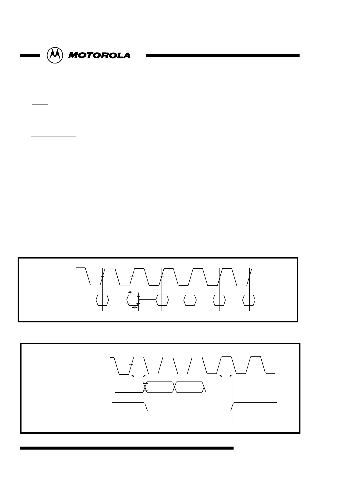
Clock
27.0Mhz is necessary. This signal on the clock pin needs to be active before the reset pin is de-asserted.
( see figures 1 and 2 )
[Function Descriptions]
Fig 1 : DVIN Data Input Timing
Input Clock 27MHz
Input Data
DVIN0~7
50%
Tds
Tdh
Clock 27MHz
Output data
H/VF sync
Output Data
TP0~8
Td
Td
Fig 2 : Sync Data Output Timing
Reset Procedure
RESET is a level sensitive input pin. Driving the RESET pin low causes a DVE reset. The 27Mhz DVE
clock signal must be active before RESET is released. De-asserting reset will latch the status of the PAL/
NTSC, TVIN and SEL pins.
The PAL/NTSC pin determines the default values for the DVE control registers. The default register
values have been chosen so that standard PAL or NTSC video will appear at the DAC outputs immediately
when a valid input digital video data stream is present.
The value on the SEL pins determine the default serial communication mode. If Low, the DVE use I2C bus
operation. If High, the DVE use 4-wired SPI operation.
After reset, the VBI signals (Closed-Caption, CGMS and WSS ) are disabled.
(see page --- for sub-address register descriptions.)
Page 6
MC44724/5 Rev 0.21 03/25/97
No.
This document contains information on a new product. Specifications and information herein are subject to change without notice.
Video Timing / Sync Generator
The DVE outputs PAL-B,D,G,H,I, PAL-N, PAL-M or NTSC-M standard video signals.
The DVE sync generator can be operated in two modes, master or slave.
In master mode, the DVE generates all the correct Horizontal and Vertical or Frame sync signals
internally, or it is output Csync signal through the EXT pin(C/Fsync).
In slave mode, the DVE derives the sync signals from the Bit-Parallel input data stream Start Active
Video (SAV) and End Active Video (EAV) data packet information. Sync signals are output on the
Hsync and F/Vsync or EXT pins and can be programmed for positive or negative polarity. The phase of
Hsync can also be controlled.
Also, the DVE allows more two slave modes. One is H/Vsync slave, and the aother is H/Fsync slave
mode.
Vertical Blanking corresponds to the following lines.
625/50 624-22 311-335 ITU-R line numbering
525/60 1-19 264-282 SMPTE line numbering
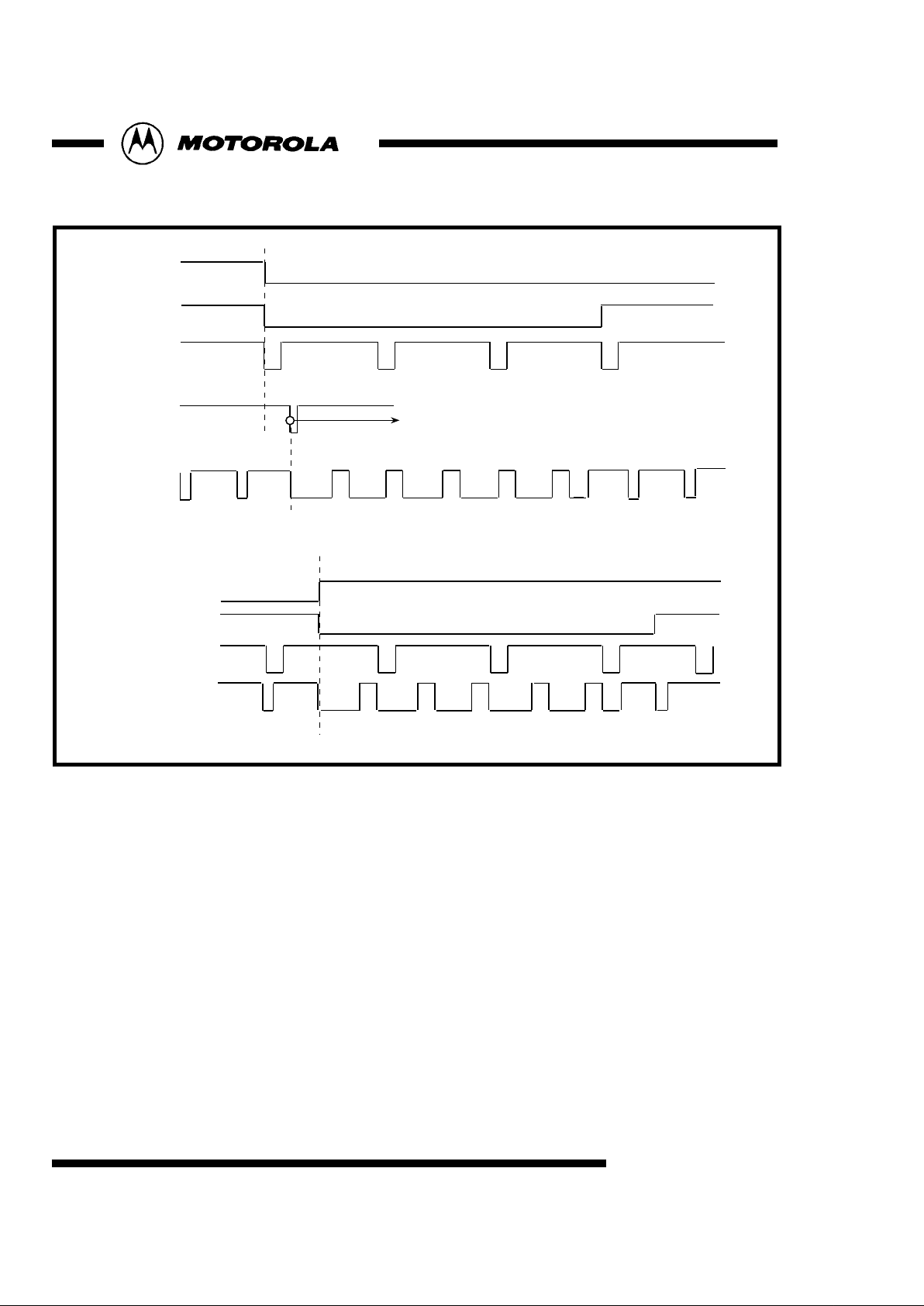
(see figures 3,4,5,6,7,8,9,10, and 11 for sub-address register descriptions.)
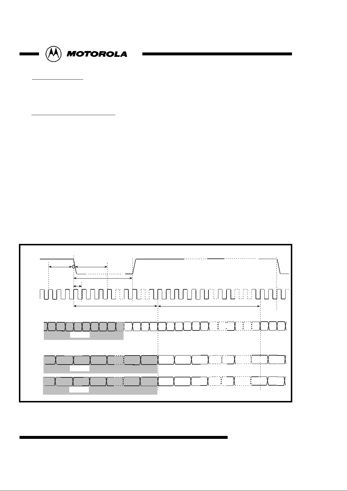
Input Data Format
The input digital video is in accord with the ITU-R Rec.656 and SMPTE 125M standards. It is an two 8-bit
or 16-bit multiplexed 4:2:2 ((CB,Y,CR)Y) data stream. Samples are latched on the rising edge of the clock
signal. Data is input on pins DVIN[ 7 : 0 ] and TP[ 8 : 1 ]
(see figures 3 and 4 for sub-address register descriptions.)
6
Fig 3 : Digital Input Timing(525/60 system) in Master Mode
70(hex){[1:0]=01}
1440T
Hsync phase
sub-address71[2:0]
Hsync
clock
128T
T
244T
Hsync polarity
sub-address71[5]
+4T delay-3T delay
DVIN0~7
Cr718
Cb718
Y718
Y719
00 00
FF
Cb2Cr0
Cb0
Y0 Y1 Y2
INVALID
00 00 XY
FF
Y718 Y719
TP1~8
Cr718Cb718
Cb2
Cr0Cb0
INVALID
DVIN0~7
Y2
Y1Y0
INVALID
16-bit input mode
8-bit input mode
Cb718Cr718
Cr2
Cr0 Cb0
or
Page 7
MC44724/5 Rev 0.21 03/25/97
No.
This document contains information on a new product. Specifications and information herein are subject to change without notice.
7
CSYNC
CSYNC
525524 1 2 3 4 5 6 7 8 9 10 11 21 22 23
262261 263 264 265 266 267 268 269 270 271 272 273 283 284 285
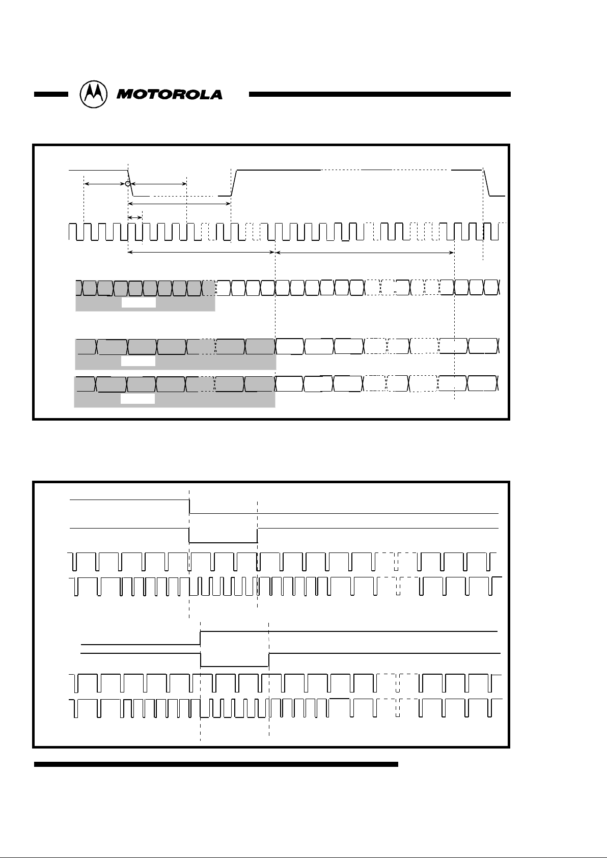
Fig 5 : Sync Timing::525/60 Interlaced System in Master Mode
Vsync
Hsync
Vsync
Hsync
sub-address71[7] =0
Fsync
Fsync polarity
sub-address71[3]
Vsync polarity
sub-address71[4]
Fsync
Fig 4 : Digital Input Timing(625/50 system) in Master Mode
70(hex){[1:0]=01}
1440T
Hsync phase
sub-address71[2:0]
Hsync
clock
128T
T
264T
Hsync polarity
sub-address71[5]
+4T delay-3T delay
DVIN0~7
Cr718
Cb718
Y718
Y719
00 00
FF
Cb2Cr0
Cb0
Y0 Y1 Y2
INVALID
00 00 XY
FF
Y718 Y719
TP1~8
Cr718Cb718
Cb2
Cr0Cb0
INVALID
DVIN0~7
Y2
Y1Y0
INVALID
16-bit input mode
8-bit input mode
Cb718Cr718
Cr2
Cr0 Cb0
or
Page 8
MC44724/5 Rev 0.21 03/25/97
No.
This document contains information on a new product. Specifications and information herein are subject to change without notice.
8
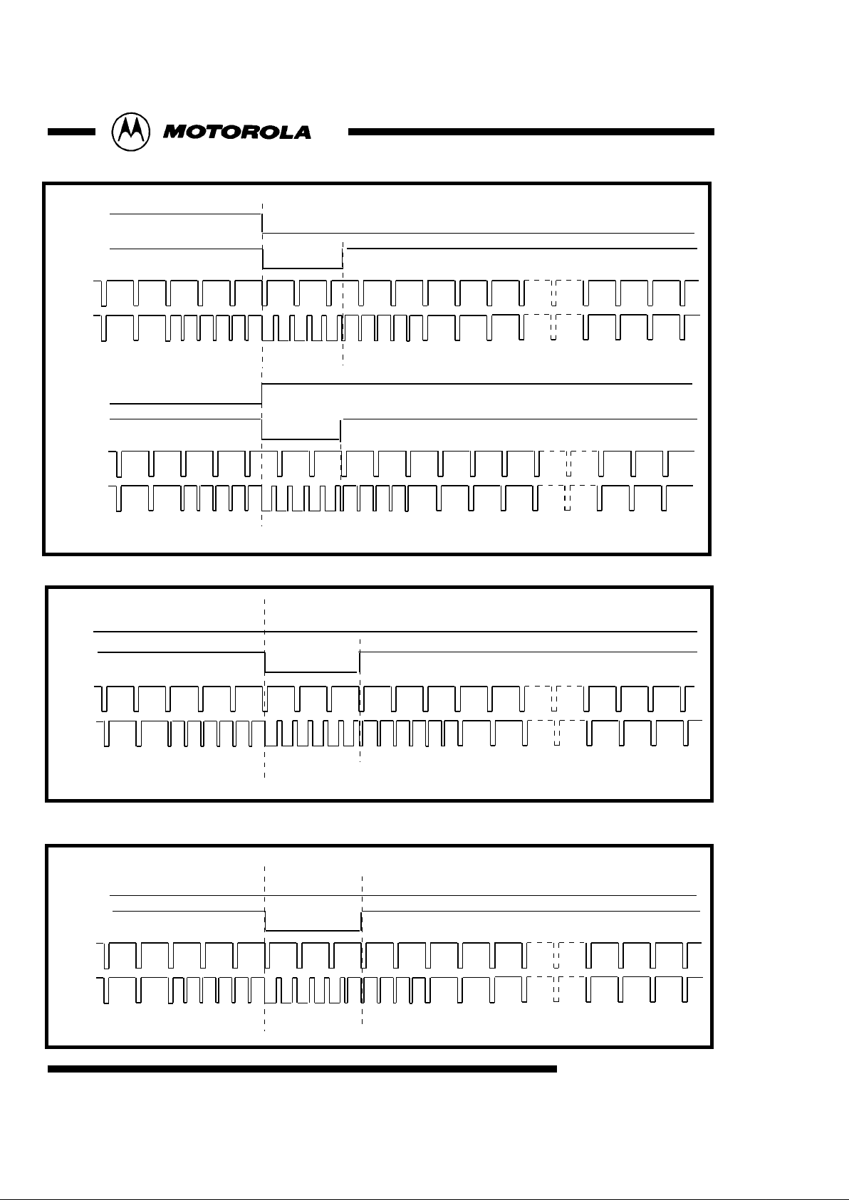
CSYNC
262261 1 2 3 4 5 6 7 8 9 10 11 21 22 23
Fig 7 : Sync Timing::525/60 Non-interlaced System in Master Mode
CSYNC
310 311 312 1 2 3 4 6 7 8
21 22 23
5309308
Vsync
Hsync
Vsync
Hsync
Fig 8 : Sync Timing::625/50 Non-interlaced System in Master Mode
9
sub-address71[7] =1
Fsync polarity
sub-address71[3]
Vsync polarity
sub-address71[4]
Fsync
Fsync polarity
sub-address71[3]
Vsync polarity
sub-address71[4]
Fsync
sub-address71[7] =1
CSYNC
623 624 625 1 2 3 4 6 7 8
21 22 23
CSYNC
311 312 313 314 315 316 317 318 319 320 321
334 335
5622621
310309
Vsync
Hsync
Vsync
Hsync
Fig 6 : Sync Timing::625/50 Interlaced System in Master Mode
9
Fsync
Fsync polarity
sub-address71[3]
Vsync polarity
sub-address71[4]
Fsync
sub-address71[7] =0
Page 9
MC44724/5 Rev 0.21 03/25/97
No.
This document contains information on a new product. Specifications and information herein are subject to change without notice.
Fig 10 : Sync Timing::525/60 Interlaced System in Slave Mode
Vsync
Hsync
Fsync
Vsync polarity
sub-address71[5]
CSYNC
3 4 5 6 7
Fsync polarity
sub-address71[4]
Odd field
CSYNC
Vsync
Hsync
Fsync
266 267 268 269
Even field
sub-address71[1:0] =10, 11
Hsync Delay
sub-address 7A[7:0], 71[3:0]
Internal Hsync
reset counter
9
Fig 9 : Analog Sync Timing::Rise and fall
2.37uS 29.41uS 27.04uS
4.74uS
0.148uS 0.148uS
63.56uS
NTSC
PAL
0.222uS
0.222uS
2.37uS
29.63uS 27.26uS
4.74uS
64.00uS
Page 10
MC44724/5 Rev 0.21 03/25/97
No.
This document contains information on a new product. Specifications and information herein are subject to change without notice.
10
Fig 11 : Sync Timing::625/50 Interlaced System in Slave Mode
Vsync
Hsync
Fsync
Vsync polarity
sub-address71[5]
Fsync polarity
sub-address71[4]
Odd field
CSYNC
625 1 2 3 4
CSYNC
Vsync
Hsync
Fsync
313 314 315 316
Even field
sub-address71[1:0] =10, 11
Hsync Delay
sub-address 7A[7:0], 71[3:0]
Internal Hsync
reset counter
Page 11

MC44724/5 Rev 0.21 03/25/97
No.
This document contains information on a new product. Specifications and information herein are subject to change without notice.
Chroma / Luma Encoding
The DVE de-multiplexes the 4:2:2 digital video data stream.
The de-multiplexed Y or Luma samples are interpolated (2X oversampled) at the clock rate. Offset
compensation is then added, next any VBI signals consisting of Closed-Caption, CGMS and WSS are
added to the appropriate lines, then finally composite sync pulses are added to the Luma signal.
(see figure 12.)
De-multiplexed component color CB and CR samples are interpolated (4X oversampled) at the clock rate.
Interpolating simplifies the output filter and allows more accurate encoding. The DVE generates the
necessary subcarrier color frequency for PAL or NTSC encoding from the 27Mhz system clock. This
color subcarrier is then modulated by the base band component color CB and CR signals to create the
video Chroma signal. (see figure 13.)
A 7.5 IRE pedestal is added for the 60Hz field rate. This can be added for the 50Hz field rate through
serial bus control. (see sub-address register descriptions)
11
CVBS and S-VIDEO or YCbCr or RGB Outputs
The internal digital video signals drive 10-bit D/A converters. Converter outputs are bi-directional current
sources where the current is proportional to the digital data with reference to the IBIAS reference current. The
pins CVBS/Cb/B, Y/G and C/Cr/R are the respective composite, Luma and Chroma or Y/Cb/Cr or R/G/B signal
current source pins. Also, each DACs can drive 75ohm load register.
User can select 2 sets of signals within above 3 sets.
(see "Application Diagram" and "sub-address register descriptions".)
Bias Current Gain
DACs can be switched off through serial bus control to reduce power consumption. Both outputs of unused
DACs should be connected to ground through a resister to avoid charge buildup.
Page 12
MC44724/5 Rev 0.21 03/25/97
No.
This document contains information on a new product. Specifications and information herein are subject to change without notice.
Fig 12 : Luminance Output Range
12
212
32
470
420
340
290
162
82
32
Digital Y input code(16~235)
525/60 and 625/50 system
100%amplitude,100%saturation color bar
0
7.5
30
41
59
70
89
100
-40
IRE
670
620
540
490
412
362
282
232
12
232
Analog Y output level(525/60 system)
100%amplitude,100%saturation color bar
0
code
1023
200
0
11
30
41
59
70
89
100
-43
IRE
670
620
540
490
412
362
282
232
44
232
Analog Y output level(625/50 system)
100%amplitude,100%saturation color bar
0
code
1023
11
Page 13

MC44724/5 Rev 0.21 03/25/97
No.
This document contains information on a new product. Specifications and information herein are subject to change without notice.
13
Fig 13 : Chrominance Output Range
-59
-45
-20
20
45
59
63
IRE
Analog C output level(525/60 system)
100%amplitude,100%saturation color bar
-63
0
Å }2
2
Å }3
2
Å }3
0
Å }3
2
Å }2
2
Å }1
1
292
256
32
68
444
480
220
256
Digital Cr-input code(16~240)
525/60 and 625/50 system
100%amplitude,100%saturation color bar
32
332
108
404
180
480
256
Digital Cb-input code(16~240)
525/60 and 625/50 system
100%amplitude,100%saturation color bar
256
Å }3
0
code
511
0
1023
-63
-48
-21.5
21.5
48
63
67
IRE
Analog C output level(625/50 system)
100%amplitude,100%saturation color bar
-67
0
Å }2
2
Å }3
2
Å }3
0
Å }3
2
Å }2
2
Å }1
1
Å }3
0
code
511
0
1023
Page 14

MC44724/5 Rev 0.21 03/25/97
No.
This document contains information on a new product. Specifications and information herein are subject to change without notice.
Fig 14 : RGB Output Range for 525/60 system
0
7.5
100
-40
IRE
12
Analog B output level(525/60 system)
100%amplitude,100%saturation color bar
0
code
1023
232
200
670
0
7.5
100
-40
IRE
Analog R output level(525/60 system)
100%amplitude,100%saturation color bar
0
code
1023
232
200
670
0
7.5
100
-40
IRE
Analog G output level(525/60 system)
100%amplitude,100%saturation color bar
0
code
1023
232
200
670
Transformation
a) R = Y + 1.371 (Cr-128)
b) G = Y - 0.698 (Cr - 128) - 0.336 (Cb - 128)
c) B = Y +1.732 (Cb - 128)
14
12
12
Page 15

MC44724/5 Rev 0.21 03/25/97
No.
This document contains information on a new product. Specifications and information herein are subject to change without notice.
Fig 15 : RGB Output Range for 625/50 system
0
100
-43
IRE
44
Analog B output level(625/50 system)
100%amplitude,100%saturation color bar
0
code
1023
232
670
0
100
-43
IRE
Analog R output level(625/50 system)
100%amplitude,100%saturation color bar
0
code
1023
232
670
0
100
-43
IRE
Analog G output level(625/50 system)
100%amplitude,100%saturation color bar
0
code
1023
232
670
Transformation
a) R = Y + 1.371 (Cr-128)
b) G = Y - 0.698 (Cr - 128) - 0.336 (Cb - 128)
c) B = Y +1.732 (Cb - 128)
15
44
44
Page 16

MC44724/5 Rev 0.21 03/25/97
No.
This document contains information on a new product. Specifications and information herein are subject to change without notice.
Closed-Caption Encoding
Closed-Captioned or Extended Data Service signals can be encoded by the DVE onto output video line 21/284
(NTSC) and line 22/335 (PAL). The CC data is input through the serial bus interface. Two 8-bit byte data pairs
are encoded for each field. There are four registers for holding the data - two bytes per field. The serial data is
7bit US-ASCII MSB first, proceeded by an odd parity bit. Total 8-bits. (P-7-6-5-4-3-2-1-0)
The DVE automatically generates the required clock run in and start bit for CC encoding. (see figure 16.)
When Closed-Captioning is enabled, the system micro processor (uP) should update the CC data once each
frame. The system uP should also write NULL characters when there is no CC data to encode. It is also
recommended to write CC data only to the inactive frame. Field1 and Field2 data are double-buffered by the
Frame sync falling edge of previous Frame, updating Frame 2 data during Frame1 display and Frame1 data
during Frame2 display.
(see figures 20 for sub-address register descriptions.)
Copy Generation Managment System (CGMS) Encoding
CGMS signals can be encoded by the DVE onto output video line 20 (525 / 60 for Japan).
CGMS identification signals also identify and control the TV screen presentation mode - wide screen,
letterbox and or normal -16:9 or 4:3.
(see figures 18 for sub-address register descriptions.)
16
Wide Screen Signalling (WSS) Encoding
WSS signals can be encoded by the DVE onto output video line 23 (625 / 50 for Europe).
WSS identification signals also identify and control the TV screen presentation mode - wide screen,
letterbox and or normal -16:9 or 4:3.
(see figures19 for sub-address register descriptions.)
Page 17

MC44724/5 Rev 0.21 03/25/97
No.
This document contains information on a new product. Specifications and information herein are subject to change without notice.
Serial Control Bus
Control of the DVE device is accomplished through the I2C-Bus or SPI serial bus.
In I2C mode, pins SDA and SCL are the respective data and clock signals. Device address can be
40(hex)/41(hex) or 1E(hex)/1F(hex) . Slave address is chosen at reset by the state of the ChipA pin
signal { 0 : 40(hex)/41(hex), 1 : 1E(hex)/1F(hex) }
Sub-address register read and write operations are documented in the following section.
In SPI mode, pins SO, SI, SCK and SEL are the respective data input, output, serial clock and chip
select signals. Register read and write operations are documented in the following section.
17
MACROVISIONTM Copy Protection
When enabled, the Luma and Chroma signals are modified according to the MACROVISIONTM copy
protection process for Pay Per View (PPV) applications revision 7.01 dated Sep 6th , 1996.
Enabling and control is through the serial control bus.
No parts will be sent to the customer until the customer provides MOTOROLA with written confirmation of
a license, non-disclosure or waiver from MACROVISIONTM.
If your customer would NOT like to use this feature or customer do NOT have an agreement of the copy
protection with MACROVISION, and then you should recommend the MC44723FT (no copy guard part).
Page 18

MC44724/5 Rev 0.21 03/25/97
No.
This document contains information on a new product. Specifications and information herein are subject to change without notice.
18
Fig 16-a : I2C-BUS Interface Write operation Timing
MSB
D7 D6 D5 D4 D3 D2 D1 D0
LSB
SCL
SDA
MSB
D7 D6 D5 D4 D3 D2 D1 D0
LSB
MSB
D7 D6 D5 D4 D3 D2 D1 D0
LSB
SCL
SDA
MSB
D7 D6 D5 D4 D3 D2 D1 D0
LSB
Start
chip address(write)
ACK
Sub-address
Data 1 Data N
ACK
ACK
ACK
Stop
MSB
D7 D6 D5 D4 D3 D2 D1 D0
LSB
SCL
SDA
MSB
D7 D6 D5 D4 D3 D2 D1 D0
LSB
MSB
D7 D6 D5 D4 D3 D2 D1 D0
LSB MSB
D7 D6 D5 D4 D3 D2 D1 D0
LSB
Start
chip address(write)
ACK
Sub-address
Data 1
ACK
ACK by MCU
ACK
Stop
SCL
SDA
Start
chip address(Read)
MSB
D7 D6 D5 D4 D3 D2 D1 D0
LSB MSB
D7 D6 D5 D4 D3 D2 D1 D0
LSB
Data N
ACK by MCU
ACK by MCU
Stop
SCL
SDA
Data 2
Fig 16-b : I2C-BUS Interface Read operation Timing
Page 19

MC44724/5 Rev 0.21 03/25/97
No.
This document contains information on a new product. Specifications and information herein are subject to change without notice.
19
Fig 17-a : SPI-BUS Interface Write operation Timing
MSB
D7 D6 D5 D4 D3 D2 D1 D0
LSB
SCK
SI
MSB
D7 D6 D5 D4 D3 D2 D1 D0
LSB
MSB
D7 D6 D5 D4 D3 D2 D1 D0
LSB
SCK
SI
MSB
D7 D6 D5 D4 D3 D2 D1 D0
LSB
Start
Write Command Sub-address
Data 1 Data N
SEL
x
SEL
MSB
x x x x x x x x
LSB
SO
(Don't
care)
MSB
x x x x x x x x
LSB
x
MSB
D7 x x x x x x x
LSB
SO
(Don't
care)
MSB
x x x x x x x x
LSB
Page 20

MC44724/5 Rev 0.21 03/25/97
No.
This document contains information on a new product. Specifications and information herein are subject to change without notice.
MSB
D7 D6 D5 D4 D3 D2 D1 D0
LSB
SCK
SI
MSB
D7 D6 D5 D4 D3 D2 D1 D0
LSB
MSB
D7 D6 D5 D4 D3 D2 D1 D0
LSB MSB
x x x x x x x x
LSB
Start
Write Command Sub-address
Data 1
Stop
SCK
SI
Start
Read Command
MSB
x x x x x x x x
LSB MSB
x x x x x x x x
LSB
Data N
Stop
SCK
SI
Data 2
Fig 17-b : SPI-BUS Interface Read operation Timing
SEL
x
MSB
x x x x x x x x
LSB
SO
(Don't
care)
MSB
x x x x x x x x
LSB
x
SEL
x
MSB
x x x x x x x x
LSB MSB
D7 D6 D5 D4 D3 D2 D1 D0
LSB
SO
x
SEL
MSB
D7 D6 D5 D4 D3 D2 D1 D0
LSB MSB
D7 D6 D5 D4 D3 D2 D1 D0
LSB
SO
20
Page 21

MC44724/5 Rev 0.21 03/25/97
No.
This document contains information on a new product. Specifications and information herein are subject to change without notice.
21
[Specifications]
Maximum Ratings
DC Supply Voltage Vdd -0.5 ~ +7.0 V
Input Voltage, All Inputs Vin -1.5 ~ Vdd+1.5 V
Output Voltage, All Outputs Vout -0.5 ~ Vdd+1.5 V
DC Output Current, per Pin Iout 25 mA
Power Dissipation Pd 750 mW
Storage Temperature Tstg -65 ~ +150 Å é
Electrical Characteristics
Characteristic Symbol Min Typ Max Unit
Power Supply Voltage(Analog Blocks) AVDD 3.1 3.3 3.5 V
DAVDD 4.75 5.0 5.25
Power Supply Voltage(Digital Blocks) DVDD 3.1 3.3 3.5 V
DVDD
Supply Current(Analog Blocks) AIcc - 30 - mA
Supply Current(Digital Blocks) DIcc - 170 - mA
Operating Temperature Ta 0 - 70 Å é
DAC Blocks Characteristics(Power Supply 3.3V,Ta=25 Å é Å }3Å é )
Characteristics Symbol Min Typ Max Unit Other
Resolution - - - 10 Bit
Integral Non-Linearity INL - - Å }4.0 LSB Vref = 1.1V
Differential Non-Linearity DNL - - Å }2.0 LSB Vref = 1.1V
Analog Output Voltage Vyo 0.85 1.00 1.15 Vp-p Vref = 1.5V
Full Scale Output Voltage Vyfs 0.85 1.00 1.15 V
Zero Scale Output Voltage Vyzs - 0.0 0.1 V
External Load Resistance RL 75 120 - É ∂
DAC Blocks Characteristics(Power Supply 5.0V,Ta=25 Å é Å }3Å é )
Characteristics Symbol Min Typ Max Unit Other
Resolution - - - 10 Bit
Integral Non-Linearity INL - - Å }4.0 LSB Vref = 1.5V
Differential Non-Linearity DNL - - Å }2.0 LSB Vref = 1.5V
Analog Output Voltage Vyo - 1.5 2.0 Vp-p Vref = 2V
Full Scale Output Voltage Vyfs - 1.5 2.0 V Vref = 2V
Zero Scale Output Voltage Vyzs - 0.0 0.1 V
External Load Resistance RL 75 240 - É ∂
Page 22

MC44724/5 Rev 0.21 03/25/97
No.
This document contains information on a new product. Specifications and information herein are subject to change without notice.
22
Tds
50
Å
Tdh
Tr
Tf
Clock
Input Data
50
Å
validnot valid not valid
Clock Blocks Characteristics
Characteristic Symbol Min Typ Max Unit
Clock Rate fc - 27.0 - MHz
Clock Duty Cycle Dty 45 50 55 Å ì
Digital Blocks Electrical Characteristics(Power Supply 3.3V,Ta=25 Å é Å }3Å é )
Characteristics Symbol Min Typ Max Unit
Input Voltage HIGH ViH 2.0 - - V
LOW ViL - - 0.8 V
Output Voltage HIGH VoH 2.4 - - V
(2.0mA) LOW VoL - - 0.4 V
Input Leakage Current Iin - Å }2.5 - É A
Hi-Z Leakage Current Ioz - Å }20 - É A
Input Capacitance Cin - - 20 pF
Load Capacitance CL - - 20 pF
Data Setup Time Tds 4 - - nS
Data Hold Time Tdh 5 - - nS
Input Rise Time Tr - - 5 nS
Input Fall Time Tf - - 5 nS
Data delay Td - - 27 nS
[Specifications]
IIC/SPI-BUS Blocks Characteristics(Power Supply 3.3V,Ta=25 Å é Å }3Å é )
Characteristics Symbol Å @Min Typ Max Uni
t
Input Voltage LOW VILM - - 0.8 V
Input Voltage High VIHM 2.3 - - V
Input Current VIM - - Å }10 É A
SDA Output Voltage (IOM=3mA) VOM - - 0.4 V
Output Current (during acknowledge) IOM 3 - - mA
Page 23

MC44724/5 Rev 0.21 03/25/97
No.
This document contains information on a new product. Specifications and information herein are subject to change without notice.
[I2C-BUS Slave Address 40(hex)/41(hex) or 1E(hex)/1F(hex)]
<I2C-Bus Format>
WRITE MODE
DATA N
DATA 0
Sub Address
Slave Address --------S
A A A A P
if more than 1byte DATA is transmitted,
then auto-increment of the Sub Address is performed
S Start condition
Slave Address 40(hex) or 1E(hex)
A Acknowledge, generated by the slave
Sub Address Sub address byte
DATA 0 First data byte
DATA N continued data byte(Sub Address is auto increment)
P Stop condition
READ MODE
Slave Address Sub Address NS A A P
Slave Address
S APDATA NAMDATA N + 1 AM
--------- AM
then
Slave receiver
Slave transmitter
40(hex) or 1E(hex)
41(hex) or 1F(hex)
40(hex) or 1E(hex)
S Start condition
Slave Address Slave receiver is act transmitter is ad
A Acknowledge, generated by the slave
Sub Address N Sub Address byte
DATA N DATA byte of Register N
DATA N + 1 DATA byte of Register N + 1 (address auto-increment)
AM Acknowledge, generated by the micro controller
P Stop condition (When Last AM must be '1' )
23
Page 24

MC44724/5 Rev 0.21 03/25/97
No.
This document contains information on a new product. Specifications and information herein are subject to change without notice.
<SPI-Bus Format>
WRITE MODE
DATA N
DATA 0
Sub Address
Write Command --------
S
P
if more than 1byte DATA is transmitted,
then auto-increment of the Sub Address is performed
S Chip select on ( Hi to Lo)
Write Command 40(hex) or 1E(hex)
Sub Address Sub address byte
DATA 0 First data byte
DATA N continued data byte(Sub Address is auto increment)
P Chip select off (Lo to Hi)
READ MODE
Write Command
Sub Address N
S P
Read Command
S P
DATA N DATA N + 1
---------
then
Slave receiver
Slave transmitter
40(hex) or 1E(hex)
41(hex) or 1F(hex)
40(hex) or 1E(hex)
S Chip select on (Hi to Lo)
Sub Address N Sub Address byte set
Read Command 41(hex) or 1F(hex)
DATA N DATA byte of Register N
DATA N + 1 DATA byte of Register N + 1 (address auto-increment)
P Chip select off (Lo to Hi)
24
[SPI-BUS]
Page 25

MC44724/5 Rev 0.21 03/25/97
No.
This document contains information on a new product. Specifications and information herein are subject to change without notice.
25
[Register Mapping and Description]
Sub-address 70 : Variable I/O Switch (write/read)
MSB LSB
Register 70
bs-off
self-SW
color bar
select
VBLK SW
EXTsync
SW
default : 0000_0001(bin)
F/Vsync SWM/S
mode1
M/S
mode0
bs - off : color burst control switch On/Off
0 : color burst ON (default)
1 : color burst OFF
self - SW : internal self H/V counter reset switch On / Off
0 : self counter reset OFF (default)
1 : self counter reset ON
Note : this mode is ONLY valid at when 70h[1: 0] is "10(bin)" or "11(bin)".
color bar select : color bar select
Luma Chroma
0 : color bar 100% 100%
1 : color bar 100% 75%
VBLK SW : Vertical Blanking Mask Enabale switch On-Off
0 : reject VBI information data in vertical blanking period (default)
1 : through VBI information data in vertical blanking period
EXTsync SW : Composite sync/Flame sync output switch
0 : Frame sync output (default)
1 : compsite sync output
F/Vsync SW : Flame sync /Vertical sync output switch
0 : Vertical sync output (default)
1 : Frame sync output
M/S sync mode1 : Master or Slave sync mode
M/S sync mode0 00 : 656 slave or H/V master mode
01 : 656 slave mode(no H/Vsync output) (defalt)
10 : Fsync/Hsync slave mode
11 : Vsync/Hsync slave mode
Page 26

MC44724/5 Rev 0.21 03/25/97
No.
This document contains information on a new product. Specifications and information herein are subject to change without notice.
Sub-address 71 : Sync control (write/read)
MSB LSB
Register 71
non-inter VBI SW
h-polarity
v-polarity
default : 0000_0100(bin)
f-polarity h- delay2 h-delay1 h-delay0
non-inter : non-interlaced mode select
0 : interlace mode (default)
1 : non-interlace mode
VBI SW : vertical blanking information signal input control switch on EXT pin
0 : VBI input Off (default)
1 : VBI input On
h-polarity : polarity of Hsync
0 : negative (default)
1 : positive
v-polarity : polarity of Vsync
0 : negative (default)
1 : positive
f-polarity : polarity of Fsync
0 : field1 (odd) = low level (default)
1 : field1 (odd) = high level
h-delay2 : delay on Hsync with referance to DVIN data in Master mode
h-delay1 000: + 4 clock delay
h-delay0 001: + 3 clock delay
010: + 2 clock delay
011: + 1 clock delay
100: + 0 clock delay
101: - 1 clock delay
110: - 2 clock delay
111: - 3 clock delay
Note : this h-delay can be also related with 7A[7:0] register and can
delay totally +2023 clock delay in H/V or H/Fsynnc slave mode.
26
Page 27

MC44724/5 Rev 0.21 03/25/97
No.
This document contains information on a new product. Specifications and information herein are subject to change without notice.
Sub-address 72 : PAL/NTSC setup (write / read)
MSB LSB
Register 72
phase-set
EXT I/O
SW
color bar
setup75 625/525
PAL/
NTSC2
PAL/
NTSC1
default : 0000_1000(bin) NTSC (If "PAL/NTSC" pin is LOW level)
0000_0101(bin) PAL
TEST
phase-set : color sub-currier phase syncronization
0 : free running (default)
1 : 1 phase reset/8 field and 1 phase reset/4 flam
TSET : for test, should be "0"
EXT I/O SW : Input/Output switch on EXT pin
0 : VBI input(default)
1 : Csync or Flame sync output
color bar : internal color bar genarator control
0 : nomal operation (default)
1 : color bar genarator On
(need to set color bar mode on sub-address 70[5]. )
setup75 : Setup level for Luminance
0 : setup level for luminunce = 0IRE
1 : setup level for luminunce = 7.5IRE
625/525 : control line mode
0 : 525 lines / 60 Hz mode
1 : 625 lines / 50 Hz mode
PAL/NTSC2 : subcarrier control
PAL/NTSC1 00 : NTSC(M)
01 : PAL (BDGHI)
10 : PAL (M)
11 : PAL (N)
27
Page 28

MC44724/5 Rev 0.21 03/25/97
No.
This document contains information on a new product. Specifications and information herein are subject to change without notice.
28
Sub-address 73: Vertical Blanking Information Luma (Y) Level (write only)
MSB
LSB
Y7 Y6 Y5 Y4 Y3 Y2 Y1 Y0
MSB
LSB
U7 U6 U5 U4 U3 U2 U1 U0
Register 73
Register 74
Sub-address 74: Vertical Blanking Information Chroma (U) Level (write only)
MSB LSB
V3
V2 V1 V0
V6 V5 V4
Register 75
V7
Sub-address 75: Vertical Blanking Information Chroma (V) Level (write only)
default : 1000_0000(bin)
default : 79(dec)
(NTSC)
157(dec) (PAL)
default : 128(dec) (NTSC)
107(dec) (PAL)
Page 29

MC44724/5 Rev 0.21 03/25/97
No.
This document contains information on a new product. Specifications and information herein are subject to change without notice.
Sub-address 76 : signal control 1(write only)
MSB LSB
Register 76
Cr Cb
Luma
CVBS dac
default : 0000_0000(bin)
C dac Y dac
Cr : Cr/Cb signal control
Cb 0 : Cr, Cb On (default)
1 : chrominance Off
Luma : luminance control
0 : luminance On (default)
1 : luminance Off
CVBSdac : D/A converter (1) output On-Off control
Cdac 0 : CVBS/Cb/BDAC1, C/Cr/RDAC1, Y/GDAC1 output On (default)
Ydac 1 : CVBS/Cb/BDAC1, C/Cr/RDAC1, Y/GDAC1 output Off
dac sw1 : 1~9-pin's D/A converter output signal control
dac sw0 01 or 11 : R/G/B output On
10 : Y/Cr/Cb output On
00 : Y/C/CVBS output On
dac sw1 dac sw0
29
Sub-address 77 : signal control 2 (write only )
MSB LSB
Register 77
B R
G
B dac R dac
G dac dac sw4
dac sw3
B : B/R/G signal control
R 0 : B/R/G signal On (default)
G 1 : B/R/G signal Off
Bdac : D/A converter (2) output On-Off control
Rdac 0 : CVBS/Cb/BDAC2, C/Cr/RDAC2, Y/GDAC2 output On (default)
Gdac 1 : CVBS/Cb/BDAC2, C/Cr/RDAC2, Y/GDAC2 output Off
dac sw4 : 17~25-pin's D/A converter (2) output signal control
dac sw3 01 or 11 : R/G/B output On (default)
10 : Y/Cr/Cb output On
00 : Y/C/CVBS output On
default : 0000_0001(bin)
Page 30

MC44724/5 Rev 0.21 03/25/97
No.
This document contains information on a new product. Specifications and information herein are subject to change without notice.
30
h-delay10 : delay on Hsync with reference to DVIN data
h-delay9 0000_0000_000 : Hsync delay 0 delay
h-delay8 to
h-delay7 1111_1111_000 : Hsync delay +255 delay
h-delay6
h-delay5
h-delay4
h-delay3
Note : this h-delay can be also related with 71[3:0] register and can
delay totally +2023 delay(1111_1111_111) in H/V or H/ Fsync
slave mode.
Sub-address 7A : Hsync delay control (write only)
MSB LSB
Register 7A
H-dela10 H-delay9
H-delay8
H-delay7
default : 0000_0000(bin)
H-delay6 H-delay5 H-delay4
H-delay3
Sub-address 78~79 : Sub-carrier phase control (write only)
MSB LSB
Register 78
sc-ph9 sc-ph8
sc-ph7
sc-ph6
default : 0000_0000(bin)
sc-ph5
MSB LSB
Register 79
default : 0000_0000(bin)
sc-ph9 : sub-currier phase control
sc-ph8 0000_0000 : sub-currier phase 0 degree (default)
sc-ph7 to
sc-ph6 1111_1111 : sub-currier phase 359 degree
sc-ph5
sc-ph4
sc-ph3
sc-ph2
sc-ph1
sc-ph0
sc-ph4 sc-ph3
sc-ph2
sc-ph1
sc-ph0
- - - - -
-
Page 31

MC44724/5 Rev 0.21 03/25/97
No.
This document contains information on a new product. Specifications and information herein are subject to change without notice.
31
Sub-address 7B : Digital Video Input Select Control (write only)
MSB LSB
Register 7B
- -
Cr _tmg 2
Cr_tmg1
default : 0000_0000(bin)
Y_tmg
Cr/Cb_tmg2 : Cr/Cb clock timing delay in 16-bit Digital Input Mode
Cr/Cb_tmg1 00 : Cr clock delay 0 clock (default)
01 : Cr clock delay +1 clock
10 : Cr clock delay +2 clock
11 : Cr clock delay +3 clock
Y_tmg : Y clock timing delay in 16-bit Digital Input Mode
0 : Y clock delay 0 clock (default)
1 : Y clock delay +1 clock
16-bit : 16-bit Multiplexed CbYCrY Digital Video Input mode
input mode 0 : 8-bit CbYCrY Digital Video Input mode (default)
1 : 16-bit CbYCrY Digital Video Input mode
16-bit
input mode
Cb _tmg 2 Cb_tmg1
Page 32

MC44724/5 Rev 0.21 03/25/97
No.
This document contains information on a new product. Specifications and information herein are subject to change without notice.
32
Sub-address 7C : signal control 3(write only)
MSB LSB
Register 7C
Ysync
R/B sync
G sync
R/B CGMS
default : 0000_0000(bin)
G CGMS RGB bf
Y sync : Y sync Signal On/Off (Y/Cb/Cr mode only)
0 : Y sync On (default)
1 : Y sync Off
R/B sync : R/B sync signal On/Off
0 : R/B sync Off (default)
1 : R/B sync On
G sync : G sync signal On/Off
0 : G sync Off (default)
1 : G sync On
R/B CGMS : R/B CGMS data Insertion On/Off
0 : CGMS data On
1 : CGMS data off
G CGMS : G CGMS data Insertion On/Off
0 : CGMS data On
1 : CGMS data off
RGB bf : RGB burst level On/Off
0 : RGB bf data On
1 : RGB bf data off
CbCr bf : CbCr burst On/Off
0 : Cb/Cr bf data On
1 : Cb/Cr bf data off
Croma : Croma burst On/Off
0 : Croma bf data On
1 : Croma bf data off
CbCr bf
Sub-address 7D~7E : Vsync delay control (write only)
MSB LSB
Register 7D
V-delay9 V-delay8
V-delay7
V-delay6
default : 0000_0000(bin)
V-delay5 V-delay4 V-delay3
V-delay2
MSB LSB
Register 7E
- -
-
-
default : 0000_0000(bin)
- - V-delay1
V-delay0
croma bf
Page 33

MC44724/5 Rev 0.21 03/25/97
No.
This document contains information on a new product. Specifications and information herein are subject to change without notice.
V-delay9 : delay on Vsync with reference to DVIN data in slave mode
V-delay8 0000_0000_000 : Vsync delay 0 delay
V-delay7 to
V-delay6 1111_1111_111 : Hsync delay +1023 delay
V-delay5
V-delay4
V-delay3
V-delay2
V-delay1
V-delay0
33
Page 34

MC44724/5 Rev 0.21 03/25/97
No.
This document contains information on a new product. Specifications and information herein are subject to change without notice.
MSB LSB
vid134 vid133 vid132 vid131
XX XX XX
Register 82
Sub-address 80~82: CGMS characters for Field1(Line20)/Field2(Line283) (write only)
NTSC only
MSB
LSB
vid118 vid117 vid116 vid115 vid114 vid113 vid112 vid111
MSB
LSB
vid128 vid127 vid126 vid125 vid124 vid123 vid122 vid121
Register 80
Register 81
b8 b7 b6 b5 b4 b3 b2 b1
b16 b15 b14 b13 b12 b11 b10
b9
b20 b19 b18 b17
XX
2.235É
11.2Å }0.6
É
49.1Å }0.5
É
b1Ref b2 b3 b4 b5 b6 b7 b8 b9 b10
b11
b12
b13
b14
b15
b16
b17
b18
b19
b20
70IRE
0IRE
-40IRE
Fig 18 : CGMS wave form
34
10.5É
Fig 19 : WSS wave form
11.0É s+-0.25
É
27.4É
38.4É
44.5É
End of
horizontal
blanking
internal
Sub-address 80~81: WSS characters for Line23 (write only)
PAL only
MSB
LSB
wss7 wss6 wss5 wss4 wss3 wss2 wss1 wss0
MSB
LSB
- -
wss13 wss12 wss11 wss10 wss9 wss8
Register 80
Register 81
b8 b7 b6 b5 b4 b3 b2 b1
b16 b15 b14 b13 b12 b11 b10
b9
500mV+-5%
Page 35

MC44724/5 Rev 0.21 03/25/97
No.
This document contains information on a new product. Specifications and information herein are subject to change without notice.
Sub-address 83~84 :closed caption characters/extended data for Field1(Line21) (write)
First byte to Encode
Register 83
Register 84
Register 85
Register 86
ccp118 ccb117 ccb116 ccb115 ccb114 ccb113 ccb112 ccb111
ccp128
ccb127 ccb126
ccb125
ccb124 ccb123 ccb122 ccb121
ccp218 ccb217 ccb216 ccb215 ccb214 ccb213 ccb212 ccb211
ccp228
ccb227 ccb226
ccb225
ccb224 ccb223 ccb222 ccb221
MSB LSB
MSB
LSB
MSB
LSB
MSB
LSB
Sub-address 85~86 :closed cation character/extended data for Field2(Line284)
Second byte to Encode
First byte to Encode
Second byte to Encode
10.50Å }0.5
É
12.91É
4.15Å }0.1
É
33.764É
b1b2b3b4b5b6b
7
p
a
r
i
t
y
b1b2b3b4b5b6b
7
p
a
r
i
t
y
CHARACTER1 CHARACTER2
parity b7 b6 b5 b4 b3 b2 b1
parity b7 b6 b5 b4 b3 b2 b1
parity b7 b6 b5 b4 b3 b2 b1
parity b7 b6 b5 b4 b3 b2 b1
50IRE
0IRE
50IRE
0IRE
-40IRE
35
Fsync
sub-address 83 & 84 and 85 & 86 (previous frame data)
are double-buffered by Flame sync falling edge
Field 1
Field 2
Fig 20 : Closed caption wave form
Fig 21 : Closed caption data update timing
default 1000_0000
Page 36

MC44724/5 Rev 0.21 03/25/97
No.
This document contains information on a new product. Specifications and information herein are subject to change without notice.
36
Sub-address 87 :Closed caption/CGMS
MSB LSB
Register 87
CC2_flag CC1_flag CC_null
-
WSS
CGMS
CC2 CC1
CC2_flag : Closed Caption Status Flag for field2/field1
CC1_flag : 00 : Automatically set to " 11 " at when 2-byte Closed
Caption data are written, and then will be cleared to "00"
when the data is send to doubled buffer
CC_null : Automatically set the null code when the data is send to doubled
buffer
0 : Keep data registers
1 : Automatically set the null code
WSS : WSS information data insertion On-Off
0 : WSS information data insertion Off
1 : WSS information data insertion On
CGMS : CGMS information data insertion On-Off
0 : CGMS information data insertion Off
1 : CGMS information data insertion On
CC2 : closed caption/extended data for field2 encoding On-Off
0 : closed caption/extended data for field2 encoding Off
1 : closed caption/extended data for field2 encoding On
CC1 : closed caption/extended data for field1 encoding
0 : closed caption/extended data for field1 encoding Off
1 : closed caption/extended data for field1 encoding On
default 00h
Page 37

MC44724/5 Rev 0.21 03/25/97
No.
This document contains information on a new product. Specifications and information herein are subject to change without notice.
37
70h:[7] burst control (default 0:on)
[6] self counter reset switch (default 0:off)
[5] color bar select (defalut 0:Luma 100% Chroma 100%)
[4] vertical blanking switch(default 0:off)
[3] EXT pin output mode select (Csync:1, Flame sync:0)
[2] F/Vsync select(default 0:Vsync)
[1:0] Master/Slave mode select(default 01:656_slave)
71h:[7] interlaced / non-interlaced
(default 0:interlaced)
[6] VBI input control on EXT pin (default 0:off)
[5] horizontal sync polarity (default 0)
[4] vertical sync polarity (default 0)
[3] flame sync polarity (default 0)
[2:0] hsync delay control (default 100:0 clock delay)
(In slave mode can use with 7A[7:0])
72h:[7] sub-currier phase syncronaiation(default 0)
[6] Test mode (default 0:off)
[5] EXT I/O switch(defalt 1:cysnc output)
[4] color bar generate(default 0:off)
[3] setup level control(default 1:7.5IRE)
[2] 625lines50Hz/525Lines60Hz
(default set PAL/NTSC pin)
[1:0] PAL/NTSC (default set PAL/NTSC pin)
00:NTSC/M
01:PAL/BGHL
(10:PAL/M) (11:PAL/N)
73h[7:0] Y_register(default 80h)
74h[7:0] U_register(default 79d:ntsc/157d:PAL)
75h[7:0] V_register(default 128d:ntsc/107d:PAL)
76h[7] Cr on/off (default 0:on)
[6] Cb on/off (default 0:on)
[5] Luma on/off(default 0:on)
(default 0: on)
[4:2] CVBS dac/Cdac/Ydac on/off(default 0: on)
[1:0] D/A converter output signal control
(default 00 : CBVS/Y/C output)
77h[7:5] B/R/G signal control (default 0: On)
[4:2] D/A converter(2) output On/Off control(default 0: On)
[1:0] D/A converter(2) output signal control(default 0X: On)
78h[7:0] sub-currier phase control(default 00h)
79h[1:0] sub-currier phase control(default 00)
79h[7:2] n.a.
7A[7:0] hsync-delay control
(In slave mode, is valid with 71h[2:0] register)
7B[7:6] n.a
[5:2] Cr/Cb clock timing delay in 16-bit digital input mode
(default 00: clock delay 0)
[1] Y clock timing delay in 16-bit digital input mode
(default 0: clock delay 0)
[0] 16-bit multiplexed CbYCrYdigital video input mode
(default 0: 8-bit YCrCb digital video input mode)
7C[7] Ysync signal On/Off(YCrCb mode only)(default 0: On)
[6] R/Bsync signal On/Of(default 0: Off)
[5] Gsync signal On/Of(default 0: Off)
[4] R/B CGMS data insertion On/Of(default 0: On)
[3] G CGMS data insertion On/Of(default 0: On)
[2:1] RGB/CbCr burst On/Off(default 0: On)
[0] Chroma burst On/Off(default 0: On)
7D[7:0] delay on Vsync with reference to DVIN data in slave
mode
7E[7:2] n.a
[1:0] delay on Vsync with reference to DVIN data in slave
mode
80~82h CGMS characters for field1(line20)/field2(line283)
80~81h WSS characters for field1(line23)
83h[7:0] CC character1(line21) (default 'h80)
84h[7:0] CC character2(line21) (default 'h80)
85h[7:0] CC character1(line284) (default 'h80)
86h[7:0] CC character2(line284) (default 'h80)
87h[7:6] Closed Caption Status Flag for field2
[5] Automatic set to null code(Closed Caption data)
[4] n.a.
[3] WSS information data insetion on/off (default 0: off)
[2] CGMS on/off (default 0: off)
[1] CC closed caption/extended data for field2 encoding
(default 0: off)
[0] CC closed caption/extended data for field1 encoding
(default 0: off)
I2C-BUS Slave Receiver Sub-address map
** WRITE MODE **
S | Slave_address(W) | A | Sub_address | A | Data0 | A | ... | DataN | A | P
S Start condition
Slave_address 42(hex) or 1C(hex)
A Acknowledge generated by me
Sub_address Sub_address register
Data0 First data
DataN Continued data(address is auto incremented)
P Stop condition
<<<<<<<< SPI-Bus Format >>>>>>
** WRITE MODE **
S | Write Command | Sub_address | Data0 | ... | DataN | P
S Chip select on (High to Low)
Write Command 42(hex) or 1C(hex)
Sub_address Sub_address byte
Data0 First data
DataN Continued data byte(address is auto incremented)
P Chip select off (Low to High)
<<<<<<<< M-BUS Format >>>>>>
Page 38

MC44724/5 Rev 0.21 03/25/97
No.
This document contains information on a new product. Specifications and information herein are subject to change without notice.
CVBS / Cb / B1
Hsync
EXT
TVIN
DVIN3
DVIN4
DVIN5
DVIN6
DVIN7
DATST
TP8
TP7
TP6
TP5
DLVss
DLVdd
TP4
MC44724
MC44725
1
2
3
4
5
6
7
8
9
12
14
15
16
17
18
19
20
21
VReff1
13
24
22
10
11
36
35
34
33
32
31
30
29
28
25
27
26
23
47
46
45
44
43
42
41
40
48
37
39
38
CVBS / Cb / B1
CVBS / Cb / B1 Vdd
Y / G1
Y / G1
Y / G1 Vdd
C / Cr / R1
C / Cr /R1
C / Cr / R 1Vdd
DAVss
Ibias1
DAVdd
ChipA
TEST
SO
SDA/SI
SCL/SCK
SEL
DVss
clock
DVdd
Reset
PAL/NTSC
DVIN0
DVIN1
DVIN2
F / Vsync
TP3
TP2
TP1
TP0
VReff2
Ibias2
NC
CVBS / Cb / B2
CVBS / Cb / B2
CVBS / Cb / B2 Vdd
Y / G2
Y /2 G
Y / G 2Vdd
C / Cr / R2
C / Cr / R2
C / Cr / R2 Vdd
64
63
62
61
60
57
59
49
50
51
52
53
56
54
55
58
DVss
DVdd
DVss
DVdd
DVd
d
47 u
F
0.01u
F
MPEG
DECODER
75 0
47 u
F
0.01u
0.01
u1k
7
57575
47 u
F
0.01u
47 u
F
0.01u
47 u
F
0.01u
7
5
CVBS
7
5
Y
7
5
C
2
k
0.01
u1k2k
75
0
75
75
75
47 uF
0.01u F
47 uF
0.01u F
47 uF
0.01u F
75
CVBS
75
Y
75
C
cloc
k
10 u
F
10 0
k
I f NTSC syst em =
"
el se PAL system = "
MCU
47 uF
0.01uF
4.7k
4.7k
DLVd
d
47 u
F
0.01u
F
[ Appr ica t ion Dia gr
a
38
Page 39

MC44724/5 Rev 0.21 03/25/97
No.
This document contains information on a new product. Specifications and information herein are subject to change without notice.
Package
A
Detail A
ZD or ZE
min max
A
A1
A2
b
c
D
E
e
HD
HE
L
L1
É
y
ZD
ZE
- 1.70
0.05 0.15
1.40TYP
0.18
0.10
9.90
9.90
11.80
11.80
0.80
0
-
1.25TYP
1.25TYP
0.27
0.20
10.1
10.1
0.50
12.20
12.20
1.20
10
0.10
A1 A2
e
b
HE
E
HD
D
L1
L
c
É ∆
3
9
Det ail
A
0.50TYP
unit :
m
 Loading...