

Page 1
MC44605
Product Preview
High Safety, Latched Mode,
GreenLine
PWM Controller
for (Multi)Synchronized
Applications
The MC44605 is a high performance current mode controller that is
specifically designed for off–line converters. This circuit has several
distinguishing features that make it particularly suitable for
multisynchronized monitor applications.
The MC44605 synchronization arrangement enables operation from
16 kHz up to 130 kHz. This product was optimized to operate with
universal mains voltage, i.e., from 80 V to 280 V, and its high current
totem pole output makes it ideally suited for driving a power MOSFET.
The MC44605 protections enable a well–controlled and safe power
management. Four major faults while detected, activate the analogic
counter of a disabling block designed to perform a latched circuit
output inhibition.
Current Mode Controller
• Current Mode Operation up to 250 kHz Output Switching Frequency
• Inherent Feed Forward Compensation
• Latching PWM for Cycle–by–Cycle Current Limiting
• Oscillator with Precise Frequency Control
• Externally Programmable Reference Current
• Secondary or Primary Sensing (Availability of Error Amplifier Output)
• Synchronization Facility
• High Current Totem Pole Output
• V
Undervoltage Lockout with Hysteresis
cc
• Low Output dV/dT for Low EMI Radiations
• Low Start–Up and Operating Current
Safety/Protection Features
• Soft–Start Feature
• Demagnetization (Zero Current Detection) Protection
• Overvoltage Protection Facility against Open Loop
• EHT Overvoltage Protection (E.H.T.OVP): Detection of too High
Synchronization Pulses
• Winding Short Circuit Detection (W.S.C.D.)
• Limitation of the Maximum Input Power (M.P.L.): Calculation of
Input Power for Overload Protection
• Overheating Detection (O.H.D.): to Prevent the Power Switch from
an Excessive Heating
Latched Disabling Mode
• When one of the following faults is detected: EHT overvoltage,
Winding Short Circuit (WSCD), a too high input power (M.P.L.),
power switch overheating (O.H.D.), an analogic counter is activated
• If the counter is activated for a time that is long enough, the circuit
gets definitively disabled. The latch can only be reset by making
decrease the Vcc down to about 3 V, i.e., practically by unplugging or
turning off the SMPS.
This document contains information on a product under development. ON Semiconductor
reserves the right to change or discontinue this product without notice.
http://onsemi.com
MARKING
DIAGRAM
16
PDIP–16
P SUFFIX
16
1
Max Power Limitation
Overheating
Detection
Current Sense Input
Demagnetization
Detection Input
ORDERING INFORMATION
Device Package Shipping
MC44605P PDIP–16 25 Units/Rail
CASE 648
A = Assembly Location
WL, L = Wafer Lot
YY, Y = Year
WW, W= Work Week
PIN CONNECTIONS
V
CC
116
V
2
C
Output
3
Gnd
4
5
6
7
8
(Top View)
* Winding Short Circuit Detection
MC44605P
AWLYYWW
1
R
ref
WSCD* Program
15
Voltage Feedback Input
14
Error Amp Output
13
Disabling Block (C
12
Soft–Start Input
11
Osc Capacitor (CT)
10
Sync and
9
EHTOVP Input
)
ext
Semiconductor Components Industries, LLC, 2000
May, 2000 – Rev. 2
1 Publication Order Number:
MC44605/D
Page 2
MC44605
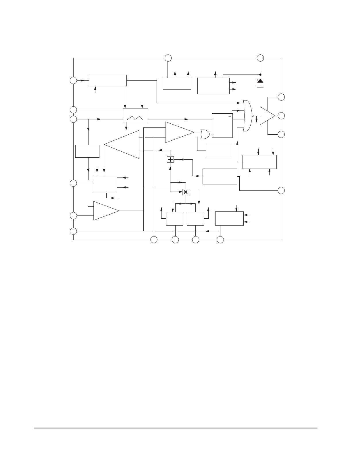
Block Diagram
Demagnetization
Detection Input
Synchronization
and EHTOVP
Input
Voltage
Feedback
Input
E/A Output
*W.S.C.D. = Winding Short Circuit Detection
8
C
T
10
9
C
12
ext
14
13
Demagnetization
Output
E.H.T.OVP
Block
V
V
ref
Management
CC
V
WSCD
Disabling
Block
+
Error
AMP
–
V
V
DT
Oscillator
Sf
W.S.C.D*
Comparator
dis
MPL
dis
OHD
Dis
out
demag out
I
ref
I
sense
I
Sense
Input
R
ref
16
i
V
ref
ref
Reference
Block
V
S
V
cs
Current
Sense
V
shift
V
cs
Sf
dis
MPL
sense
7 6
V
MPL
block
Maximum
Power
Limitation
2
cs
O.H.D.
block
Heating
Detection
Vccenable
Supply
Initialization
Block
Dis
out
Set
PWM
Latch
Reset
Thermal
Shutdown
V
Level
shift
Programmation
dis
OHD
Soft–Start
115
OverCurrent Soft–Start
Input
Q
UVLO1
UVLO2
I
ref
UVLO2
V
CC
1
18 V
Buffer
V
ref
Over Voltage
Management
V
CC
enable
UVLO1
VCCenable
MC44605
V
CC
15
V
2
C
Output
3
4
Gnd
WSCD
Programmation
http://onsemi.com
2
Page 3

MC44605
gg
OL
V
I
A
V
CC
I
Sink
mA
0.1
1.0
MAXIMUM RATINGS
Rating Pin # Symbol Value Unit
Total Power Supply and Zener Current (ICC + IZ) 40 mA
Output Supply Voltage with Respect to Ground 2
Output Current* 3 mA
Source I
Sink I
Output Energy (Capacitive Load per Cycle) W 5.0 µJ
Soft–Start V
Current Sense, Voltage Feedback, E/A Output, CT, R
WSCD
E.H.T.OVP, Sync Input Current mA
Source 9
Sink 9
Demagnetization Detection Input Current 8 mA
Source I
Sink I
Error Amplifier Output Sink Current 13 I
Power Dissipation and Thermal Characteristics
Maximum Power Dissipation at TA = 85°C P
Thermal Resistance, Junction–to–Air R
Operating Junction Temperature T
Operating Ambient Temperature T
*Maximum package power dissipation must be observed.
, MPL, OHD, C
ref
ext
,
1
6
6
V
C
V
CC
O(Source)
O(Sink)
SS
V
in
I
sync (Source)
I
(Source)
EHT
I
sync (Sink)
I
EHT (Sink)
demag–ib (Source)
demag–ib (Sink)
E/A (Sink)
D
θJA
J
A
18 V
–750
750
–0.3 to 2.2 V V
–0.3 to 5.5 V V
–4.0
10
–4.0
10
20 mA
0.6 W
100 °C/W
150 °C
–25 to +85 °C
ELECTRICAL CHARACTERISTICS (V
values TA = –25° to +85°C unless otherwise noted.) (Note 1.)
Characteristic
OUTPUT SECTION (Note 2.)
Output Voltage* 3 V
Low Level Drop Voltage (I
High Level Drop Voltage(I
Output Voltage During Initialization Phase 3 V
VCC = 0 to 1.0 V, I
= 1.0 to 5.0 V,
CC
= 5.0 to 13 V,
Output Voltage Rising Edge Slew–Rate (CL = 1.0 nF, TJ = 25°C) dVo/dT – 300 – V/µs
Output Voltage Falling Edge Slew–Rate (CL = 1.0 nF, TJ = 25°C) dVo/dT – –300 – V/µs
*VC must be greater than 5.0 V .
1. Adjust VCC above the start–up threshold before setting to 12 V . Low duty cycle pulse techniques are used during test to maintain junction
temperature as close to ambient as possible.
2. No output signal when the Error Amplifier output is in Low State, i.e., when for instance, VFB = 2.7 V.
Sink
Sink
Sink
(I
Sink
Source
(I
Source
= 10 µA
= 100 µ
= 1.0
= 100 mA)
= 500 mA)
= 200 mA)
= 500 mA)
and VC = 12 V, R
CC
= 10 kΩ, CT = 2.2 nF, for typical values TA = 25°C, for min/max
ref
Pin # Symbol Min Typ Max Unit
V
OL
V
OH
OL
–
–
–
–
– –
–
–
1.0
1.4
1.5
2.0
0.1
1.2
2.0
2.0
2.7
1.0
1.0
V
http://onsemi.com
3
Page 4

MC44605
ELECTRICAL CHARACTERISTICS (V
values TA = –25° to +85°C unless otherwise noted.) (Note 1.)
Characteristic
ERROR AMPLIFIER SECTION
Voltage Feedback Input (V
Input Bias Current (VFB = 2.5 V) 14 I
Open Loop Voltage Gain (V
Unity Gain Bandwidth BW MHz
TJ = 25°C – – –
TA = –25° to +85°C – – 5.5
Voltage Feedback Input Line Regulation (VCC = 10 V to 15 V) V
Output Current 13 mA
Sink (V
TA = –25° to +85°C
Source (V
TA = –25° to +85°C
Output Voltage Swing 13 V
High State (I
Low State (I
CURRENT SENSE SECTION
Maximum Current Sense Input Threshold
(V
Feedback (pin14)
Input Bias Current 7 I
Propagation Delay (Current Sense Input to Output at VTH of
MOS transistor = 3.0 V)
OSCILLATOR AND SYNCHRONIZATION SECTION
Frequency (TA = –25° to +85°C)
Frequency Change with Voltage (VCC = 10 V to 15 V) ∆F
Frequency Change with Temperature (TA = –25° to +85°C) ∆F
Ratio Charge Current/Reference Current (TA = –25° to +85°C) I
Free Mode Oscillator Ratio = I
Synchronization Input Threshold Voltage 9 V
Negative Clamp Level (I
UNDERVOLTAGE LOCKOUT SECTION
Start–up Threshold 1 V
Disable Voltage After Threshold T urn–On (UVLO 1)
(TA = –25° to +85°C)
Disable Voltage After Threshold T urn–On (UVLO 2)
(TA = –25° to +85°C)
1. Adjust VCC above the start–up threshold before setting to 12 V . Low duty cycle pulse techniques are used during test to maintain junction
temperature as close to ambient as possible.
= 1.5 V, VFB = 2.7 V)
E/A out
= 5.0 V, VFB = 2.3 V)
E/A out
E/A out (source)
E/A out (sink)
= 2.3 V and V
syncth–in
= 2.5 V) 14 V
E/A out
= 2.0 V to 4.0 V) A
E/A out
= 0.5 mA, VFB = 2.3 V) V
= 0.33 mA, VFB = 2.7 V) V
Soft–Start (pin11)
discharge
= 2.0 mA) NEG–SYNC –0.65 –0.5 –0.34 V
and VC = 12 V, R
CC
/(I
discharge
= 1.2 V)
+ I
charge
= 10 kΩ, CT = 2.2 nF, for typical values TA = 25°C, for min/max
ref
Pin # Symbol Min Typ Max Unit
FB
FB–ib
VOL
FBline–reg
I
Sink
I
Source
OH
OL
7 V
) D 72 75 78 %
1 V
1 V
cs–th
cs–ib
t
PLH(In/Out)
F
OSC
/∆V – 0.05 – %/V
OSC
/∆T – 0.05 – %/°C
OSC
charge/Iref
syncth
stup–th
disable1
disable2
2.4 2.5 2.6 V
–2.0 –0.6 – µA
65 70 – dB
–10 – 10 mV
2.0 12 –
–2.0 – –0.2
5.5 6.5 7.5
– 1.0 1.1
0.96 1.0 1.04 V
–10 –2.0 – µA
– 120 200 ns
16 – 20 kHz
0.39 – 0.48 –
–250 –200 –150 mV
13.6 14.5 15.4 V
8.3 – 9.6 V
7.0 7.5 8.0 V
http://onsemi.com
4
Page 5

MC44605
ELECTRICAL CHARACTERISTICS (V
values TA = –25° to +85°C unless otherwise noted.) (Note 1.)
Characteristic
REFERENCE SECTION
Reference Output Voltage (VCC = 10 V to 15 V) 16 V
Reference Current Range (I
Reference Voltage Over I
DEMAGNETIZATION DETECTION SECTION (Note 2.)
Demagnetization Detect Input 8
Demagnetization Comparator Threshold (V
Propagation Delay (Input to Output, Low to High) t
Input Bias Current (V
Minimum Off–Time when the pin 8 is grounded T
Negative Clamp Level (I
Positive Clamp Level (I
SOFT–START SECTION (Note 3.)
Ratio Charge Current/I
Discharge Current (V
Clamp Level V
Circuit Inhibition Threshold* V
VCS Soft–Start Clamp Level (R
*The circuit is shutdown if the Soft–Start pin voltage is lower than this level.
1. Adjust VCC above the start–up threshold before setting to 12 V . Low duty cycle pulse techniques are used during test to maintain junction
temperature as close to ambient as possible.
2. This function can be inhibited by connecting pin 8 to GND. In this case, there is a minimum off–time equal to T
3. The MC44605 can be shut down by connecting Soft–Start pin (pin 11) to Ground.
soft–start
= V
ref
ref/Rref
Range ∆V
ref
= 65 mV) I
demag
= –2.0 mA) CLVL–neg –0.50 –0.38 –0.25 V
demag
= +2.0 mA) CLVL–pos 0.50 0.72 0.85 V
demag
(TA = –25° to +85°C) I
ref
= 1.0 V) I
soft–start
and VC = 12 V, R
CC
, R = 5.0 k to 25 kΩ) 16 I
Decreasing) V
pin9
= 5 kΩ) V
= 10 kΩ, CT = 2.2 nF, for typical values TA = 25°C, for min/max
ref
Pin # Symbol Min Typ Max Unit
PLH(In/Out)
ref
ref
ref
demag–th
demag–lb
DEM–GND
ss–ch/Iref
discharge
SS–CLVL
SSinhi
CSsoft–start
2.4 2.5 2.6 V
–500 – –100 µA
–40 – 40 mV
50 65 80 mV
– 0.5 – µs
–0.5 – – µA
1.5 3.0 4.5 µs
0.37 – 0.43 –
1.5 5.0 – mA
2.2 2.4 2.6 V
30 – 150 mV
0.45 0.5 0.55 V
DEM–GND
.
http://onsemi.com
5
Page 6
MC44605
ELECTRICAL CHARACTERISTICS (V
values TA = –25° to +85°C unless otherwise noted.) (Note 1.)
Characteristic
OVERVOLTAGE SECTION
Propagation Delay (VCC > 18.1 V to V
Protection Level on VCC (TA = –25° to +85°C) VCC
EHT OVP SECTION (Note 2.)
Negative Clamp Level (I
EHT OVP Input Threshold V
EHT OVP Input Bias Current (V
WINDING SHORT CIRCUIT DETECTION SECTION
WSCD Threshold with I
MPL & OHD SECTION
MPL Parameter* Γ
MPL Comparator Threshold** V
OHD Parameter*** Γ
OHD Comparator Threshold**** V
*This parameter is defined in the MPL §. This parameter is obtained by measuring the MPL pin average current and dividing this result by the
corresponding squared VCS, the measured frequency value and the CT value deducted from the measured frequency value.
Measurement conditions: V
is typically equal to 18 kHz – R
**The MPL comparator output is Dis
***This parameter is defined in the OHD §. This parameter is obtained by measuring the OHD pin average current and dividing this result by
the corresponding squared VCS value and multiplying it by the R
Measurement conditions: V
is typically equal to 18 kHz – R
****The OHD comparator output is Dis
DISABLING BLOCK SECTION
Delay Pulse Width
Ratio (EHTOVP and WSCD Disabling Capacitor Charge
Current)I
Ratio (MPL and OHD Disabling Capacitor Charge Current)I
Minimum VCC Value Enabling the Disabling Block Latch* V
*Once a fault detection activated it, the Disabling Block Latch gets reset when the VCC becomes lower than this threshold.
TOTAL DEVICE
Power Supply Current
Power Supply Zener Voltage (ICC = 35 mA) V
Thermal Shutdown – – 155 – °C
*Refer to Note 1.
**This consumption is measured while the circuit is inhibited by the Definitive Latch.
1. Adjust VCC above the start–up threshold before setting to 12 V . Low duty cycle pulse techniques are used during test to maintain junction
temperature as close to ambient as possible.
2. This function can be inhibited by connecting pin 9 to GND. In this case, the synchronization block is inhibited too and the MC44605 works
in free mode.
ref
Startup–Up (VCC = 5.0 V with VCC increasing) – 0.35 0.55
Startup–Up (VCC = 9.0 V with VCC increasing) – 0.35 0.55
Startup–Up (VCC = 12 V with VCC increasing) – 0.35 0.55
Operating TA = –25°C to +85°C* – 20 25
Disabling Mode (VCC = 6.0 V)** – – 0.55
synch–in
= 200 µA Vshift 70 100 120 mV
pin15
Feedback(pin 14)
Feedback(pin 14)
out
= –2.0 mA) NEG–SYNC –0.65 –0.5 –0.35 V
EHT OVP(pin 9)
= 10 kΩ "1%, CT = 2.2 nF).
ref
MPL
= 10 kΩ "1%, CT = 2.2 nF).
ref
OHD
and VC = 12 V, R
CC
Low)
= 0 V) 9 I
= 2.3 V , V
.
= 2.3 V , V
.
soft–start(pin 11)
soft–start(pin 11)
ref
= 10 kΩ, CT = 2.2 nF, for typical values TA = 25°C, for min/max
ref
Pin # Symbol Min Typ Max Unit
T
PHL(In/Out)
prot
ref
EHTOVP
MPL
MPL–th
OHD
OHD–th
= 0.5 V and pins 7, 8, and 9 connected to GND (the working frequency
value.
ref
= 0.5 V and pins 7, 8, and 9 connected to GND (the working frequency
T
WSCD
I
Dis–H/Iref
I
Dis–L/Iref
CCDis
I
CC
Z
1.0 – 4.0 µs
15.9 – 18.1 V
7.0 7.4 7.8 V
–5.0 – 0 µA
0.185 0.240 0.295 V
2.4 2.5 2.6 V
1.15 1.50 1.85 V
2.4 2.5 2.6 V
– 4.0 – µs
90 100 110 %
2.7 3.1 3.5 %
1.0 – 5.0 V
18.5 – – V
–1
–1
mA
http://onsemi.com
6
Page 7

MC44605
Pin Name Pin Description
1 V
2 V
3 Output The output current capability is suited for driving a power MOSFET.
4 GND The ground pin is a single return typically connected back to the power
5 Maximum Power Limitation This block enables to estimate the input power. When this calculated power
6 Over–Heating Detection This block estimates the MOSFET heating. When this calculated heating is
7 Current Sense Input A voltage proportional to the current flowing into the power switch is
8 Demagnetization Detection A voltage delivered by an auxiliary transformer winding provides to the
9 Synchronization and E.H.T.OVP Input Activating the synchronization input pin with a pulse higher or equal to the
10 Oscillator Capacitor C
11 Soft–Start A capacitor connected to this pin can temporary reduce the maximum
12 C
13 E/A Output The error amplifier output is made available for loop compensation.
14 Voltage Feedback This is the inverting input of the Error Amplifier. It can be connected to the
15 Winding Short Circuit Detection
16 R
CC
C
T
(Disabling Block) When a too high synchronization pulse voltage (E.H.T.OVP) or a winding
ext
Programmation
ref
This pin is the positive supply of the IC.
The output high state, VOH, is set by the voltage applied to this pin. With a
separate connection to the power source, it gives the possibility to set by
means of an external resistor the output source current at a different value
than the sink current.
source. It is used as control and power ground.
is detected as too high, a fault information is sent to the disabling block in
order to definitively disable the circuit.
too high, the device gets definitively disabled (disabling block action).
connected to this input. The PWM latch uses this information to terminate
the conduction of the output buffer. A maximum level of 1 V allows to limit
the inductor current.
demagnetization pin an indication of the magnetization state of the flyback
energy reservoir. A zero voltage detection corresponds to a complete core
demagnetization. The demagnetization detection prevents the oscillator
from a re–start and so the circuit from a new conduction phase, if the
fly–back is not in a dead–time state. This function can be inhibited by
connecting Pin 8 to GND but in this case, there is a minimum off–time
typically equal to 3 µs.
negative threshold (typically –200 mV) allows the next switching period to
be reinitialized. The oscillator is free when connecting Pin 9 to GND.
When the E.H.T.OVP pin receives a voltage that is greater than 7.5 V, the
disabling block C
disabled if the C
incorporated to detect and disable the device when the synchronization
pulses are too high.
The free mode oscillator frequency is programmed by the capacitor C
choice together with the R
pin 10 and GND, generates the oscillator sawtooth.
inductor peak current. By this way, a soft–start can be performed. By
connecting pin 11 to Ground, the MC44605 is shut down.
short circuit (WSCD) is detected, the capacitor C
a current source I
is charged using I
the circuit is definitively disabled. Then, to restart, the converter must be
switched off in order to make VCC decrease down to about 0 V.
Switching Mode Power Supply output through an optical (or else) feedback
loop or to the subdivided VCC voltage in case of primary sensing technic.
The W.S.C.D. block is incorporated to detect the transformer Winding Short
Circuits. This function is performed by detecting the inductor overcurrents
thanks to a comparator which threshold is programmable to be well
adapted to any application.
The R
perform the precise oscillator waveform. The current range goes from 100
µA up to 500 µA.
value fixes the internal reference current that is particularly used to
ref
capacitor is charged so that the circuit gets definitively
ext
voltage becomes higher than V
ext
resistance value. CT, connected between
ref
. In the case of a MPL or OHD fault detection, C
Dis– H
Dis–L
. If the C
capacitor voltage gets higher than V
ext
. This block is
ref
is charged using
ext
T
ref
ext
,
http://onsemi.com
7
Page 8

MC44605
Summary of the Main Design Equations
The following table consists of equations enabling to dimension a multisynchronized SMPS operating in discontinuous
mode.
Lp
d
Pon
max
(V
DS
(VD)max
max
max
)
max
(ni)
Pin
+
Ipk
max
+
1
+
3
+ǒ2Ǹ
max
AL+
max
2Ǹ·Vac
ƪ
Ǹ
2
2 Pin
+
Ǹ
Ǹ
Pin
max
Rdson
+ǒ2Ǹ
+N
(N n
Pout
+
min
·Vac
min
max
2 Pin
L fsync
Lp
Vac
Vac
max
Vac
n
Vout
L
P
Vout
max
η
min
Ipk
max
N
NVo
)
NVo
fsync
max
min
fsync
max
Ǔ
)(N
Ǔ
Ipk
2
)
ƫ
max
2
)
max
2
max
d
Vout)
Vout
max
Pout
The maximum input power Pin
by the efficiency (η). In this kind of application, the efficiency is generally
taken equal to 80%.
The inductor value Lp must be chosen lower than Lp
this value (to optimize the application design–in).
In effect, if Lp was higher than Lp
working could not be guaranteed (in some cases, the demagnetization
phase would not be finished while a new conduction phase should start to
follow the synchronization).
Ipk
when the power to transfer is maximum at the minimum synchronization
frequency (60 W output, 30 kHz in the proposed application).
d
input voltage when the power demand is maximum while the
synchronization frequency also is maximum.
Pon
Ipk
This conduction losses estimation enables to dimension the power Mosfet.
(V
In fact, this calculation does not take into account the turnings off spikes.
So, it is necessary to take a margin of at least about 50 V.
(VD)max is the maximum voltage the high voltage secondary diode must
be able to face. Because of the turning off spikes, a margin must also be
taken.
(AL) and (ni) are the magnetic parameters.
(ni)
saturated when the peak current is high.
(AL) is the ferrite constant that links the primary inductor value to the
squared number of primary turns: Lp = AL x n
is the maximum power the load may draw in normal working.
max
is easily deducted by dividing Pout
max
or ideally equal to
max
, a synchronized and discontinuous
max
is the maximum inductor peak current. This current is obtained
max
is the maximum duty cycle. The duty cycle is maximum at the lowest
max
is the maximum Mosfet on–time losses that are proportional to
max
, d
max
DS
max
and Rdson (on–time Mosfet resistor).
max
)max is the maximum voltage the power switch must be able to face.
must not exceed the ferrite (ni). Otherwise, the transformer may get
2
.
p
max
Error Amplifier
A fully compensated Error Amplifier with access to the
inverting input and output is provided. It features a typical
DC voltage gain of 70 dB. The non inverting input is
internally biased at 2.5 V and is not pinned out. The
converter output voltage is typically divided down and
monitored by the inverting input. The maximum input bias
current with the inverting input at 2.5 V is –2.0 µA. This can
cause an output voltage error that is equal to the product of
the input bias current and the equivalent input divider source
resistance.
http://onsemi.com
Compensation
R
FB
C
f
R
8
+
1.0 mA
13
R
f
2.5 V
14
Voltage
Feedback
Input
R
1
2
Figure 1. Error Amplifier Compensation
Error
Amplifier
MC44605
From Power Supply Output
2R
R
1.0 V
Gnd
Current
Sense
Comparator
4
Page 9

MC44605
The Error Amp Output (Pin 13) is provided for external
loop compensation. The output voltage is offset by two
diodes drops ([1.4 V) and divided by three before it
connects to the inverting input of the Current Sense
Comparator. This guarantees that no drive pulses appear at
the Source Output (Pin 3) when Pin 13 is at its lowest state
(VOL). This occurs when the power supply is operating and
the load is removed, or at the beginning of a soft–start
interval. The Error Amp minimum feedback resistance is
limited by the amplifier’s minimum source current (0.2 mA)
and the required output voltage (VOH) to reach the current
sense comparator’s 1.0 V clamp level:
R1(min)
(3 1V))1.4 V
+
0.2 mA
+
22 kΩ
Current Sense Comparator and PWM Latch
The MC44605 operates as a current mode controller. The
circuit uses a current sense comparator to compare the
inductor current to the threshold level established by the
Error Amplifier output (Pin 13). When the current reaches
the threshold, the current sense comparator terminates the
output switch conduction that has been initiated by the
oscillator, by resetting the PWM Latch. Thus the error signal
controls the peak inductor current on a cycle–by–cycle
basis. This configuration ensures that only one single pulse
appears at the Source Output during the appropriate
oscillator cycle.
V
in
V
C
14
R
3
Current
Sense
7
2
C
Q1
R
3
R
R
S
V
demag out
Thermal
Protection
UVLO
Dis
out
VS
Current Sense
Comparator
S
Q
R
PWM
Latch
Substrate
Figure 2. Output Totem Pole
The inductor current is converted to a voltage by inserting
the ground referenced sense resistor RS in series with the
power switch Q1.
This voltage is monitored by the Current Sense Input
(Pin 7) and compared to a level derived from the Error Amp
output. The peak inductor current under normal operating
conditions is controlled by the voltage at Pin 13 where:
Ipk[
V
(pin13)
*
3 R
1.4 V
S
The Current Sense Comparator threshold is internally
clamped to 1.0 V. Therefore the maximum peak switch
current is:
I
pk(max)
+
1V
R
S
Undervoltage Lockout Section
As depicted in Figure 3, an undervoltage lockout has been
incorporated to guarantee that the IC is fully functional
before allowing the system working.
In effect, the VCC is connected to the non inverting input
of a comparator that has an upper threshold equal to 14,5 V
(typical V
V
disable 2
) and a lower one equal to 7.5 V (typical
stup–th
). This hysteresis comparator enables or disables
the reference block that generates the voltage and current
sources required by the system.
This block particularly, produces V
I
that is determined by the resistor R
ref
(pin 16 voltage) and
ref
connected between
ref
pin 16 and the ground:
V
+
1
V
7.5 V
C
V
disable1
9.0 V
ref
where V
R
ref
V
ref enable
C
START–UP
0
disable
UVLO1
STAR T–UP
14.5 V
(to SOFTSTAR T)
Figure 3. VCC Management
+
ref
10
UVLO1
2.5 V (typically)
Reference Block:
Voltage and Current
Sources Generator
(V
, I
ref
ref
MC44605
R
ref
Pin 16
, ...)
V
CC
(Pin 1)
I
ref
In addition to this, VCC is compared to a second threshold
level that is nearly equal to 9 V (V
disable1
) so that a signal
UVLO1 is generated to reset the soft start block and so, to
disable the output stage (refer to the Soft–Start §) as soon as
VCC becomes lower than V
disable 1
. In this way, the circuit
is reset and made ready for a next start–up, before the
reference block is disabled (refer to Figure 3). Thus, finally
the upper limit for the minimum normal operating voltage
http://onsemi.com
9
Page 10

MC44605
is 9.4 V (maximum value of V
hysteresis is 4.2 V. [(V
stup–th)min
disable 1
) and so the minimum
= 13.6 V].
The large hysteresis and the low start–up current of the
MC44605 make it ideally suited for off–line converter
applications where efficient bootstrap start–up techniques
are required.
Soft–Start Control Section
The Vcs value is clamped down to the pin 11 voltage.
So, if a capacitor is connected to this pin, its voltage
increases slowly at the start–up (the capacitor is charged by
an internal current source 0.4 I
). So, Vcs is limited during
ref
the start–up and then a soft–start is performed.
This pin can be used to inhibit the circuit by applying a
voltage that is lower than V
(refer to page 4).
SSinhi
Particularly , the MC44605 can be shutdown by connecting
the soft–start pin to ground.
As soon as V
V
disable1
down to V
), a signal UVLO1 is generated until the Vcc falls
dis2
is detected (that is Vcc lower than
dis1
(refer to the undervoltage lockout section §).
During the delay between the disable1 and the disable2,
using a transistor controlled by UVLO1, the pin 11 voltage
is made equal to zero in order to make the soft–start
arrangement ready to work for the next re–start.
V
ref
Vcs
Output
Inhibition
SSlnhi
Pin 11
Soft
Start
Capacitor
0.4 I
2.4 VD
Z
Figure 4. Soft–Start
ref
UVLO1
V
MC44605
Oscillator Section (Figures 5 & 5b)
The oscillator and synchronization behavior is
represented in Figure 5b.
The MC44605 oscillator achieves four functions:
— it fixes the free mode frequency
— it takes into account the synchronization signal
— it does not allow a new power switch conduction if the
flyback is not in a dead–time state when the circuit
works in demagnetization mode (pin 8 connected)
— it builds the Sf pulse required by the MPL block
During the operating mode, the oscillator sawtooth can
vary between a valley value (1.6 V typically) and a peak one
(3.6 V typically) and presents three distinct phases:
— the CT charge
— the CT discharge
— the phase during which the oscillator voltage is
maintained equal to its valley value. This happens at
the end of a discharge cycle when the synchronization
or demagnetization condition does not allow a new C
charge phase. During this sequence, I
compensates the charge current I
REGUL
charge
.
The oscillator has two working modes:
— a free one when there is no synchronization
— a synchronized one.
In the free working, the oscillator grows up from its valley
value to its peak one for the charge phase and when once the
peak value is reached, a discharge sequence makes the C
voltage decrease down to its valley value. When the
decrease phase is finished, a new charge cycle occurs if the
demagnetization condition is achieved (VDT high).
Otherwise there is a REGUL phase until VDT gets high.
In the synchronized mode, the charge cycle is only
allowed when the synchronization signal gets high while a
dead time has been detected (VDT high). This charge phase
is stopped when the synchronization signal has got low and
when the oscillator voltage is higher than V
int
, the
intermediary voltage level used to generate the calibrated
pulse Sf by comparing the CT voltage to this threshold. So,
when these two conditions are performed, a discharge
sequence is set until the oscillator voltage is equal to its
valley value. Then, the CT voltage is maintained constant
thanks to the “REGUL” arrangement until the next
synchronization pulse.
In both cases, during the charge phase, a signal VS is
generated. When Sf becomes high. VS gets high and remains
in this state until the PWN latch is set of Sf is low. Then, V
keeps low until the next Sf high level. This oscillator
behavior is obtained using the process described in
Figure 5b.
T
T
S
http://onsemi.com
10
Page 11

Inductor
current
V
DT
MC44605
a – Free mode
Oscillator
Sf
Output
Synchro
input
V
int
b – Synchronized mode
Inductor
current
V
DT
Oscillator
Sf
Output
V
int
Figure 5b. Oscillator Behavior
http://onsemi.com
11
Page 12

MC44605
In effect, the output of the latch L1 is:
— high during the oscillator capacitor charge and during
the REGUL phase
— low for the oscillator capacitor discharge
Now , the latch L2 is set when the L1 output is high and the
synchronization condition is performed (that is: sync = 1 –
free mode or synchro signal high state) and during the
dead–time (VDT high). So, this latch is set for the CT charge.
On the other hand, this latch is reset by the signal used to
reset L1. Consequently, it is reset at the end of the charge
phase.
So, in any case, QL2 is:
— high during the CT charge cycle
— low in the other cases
Thus, this latch enables to obtain a signal that is high for
the charge phase and low in the other cases, whatever the
mode (synchronized or free) and whatever the
synchronization pulses width (higher than the delay
necessary for the oscillator to reach its intermediary value or
lower than this delay) in the synchronized mode.
That is why:
— the discharge current source must be connected to the
oscillator capacitor when QL1 is low. The condition
(CT voltage higher than the valley value) is added to
stop the discharge phase as soon as the oscillator
voltage is detected as lower than the valley value
(without any delay due to the L1 latch propagation
time).
— the REGUL current source must be connected when:
• QL1 is high (charge or REGUL phase)
• QL2 is low (the oscillator is not in a charge phase)
On the other hand, the oscillator charge is stopped when:
— the oscillator voltage reaches the peak value in the
free mode
— the oscillator voltage is higher than the intermediary
value (V
) and the synchronization signal is negative,
int
in the synchronized mode.
Consequently, in any case, QL2 that is high during the
oscillator charge phase, is high for the delay during which
the oscillator voltage grows from the valley value up to the
intermediary one. That is why the signal Sf (refer to the MPL
block) that must be high when the oscillator voltage is
between the valley value and the intermediary one during
the charge phase (QL2 high), is obtained using an AND gate
with the following inputs:
—QL2 (QL2 high <=> charge phase)
—C
OSCINT
(C
OSCINT
high <=> the CT voltage is lower
than the intermediary value).
So, using the output of this AND gate, Sf is obtained.
This signal Sf is connected to a logic block consisting of
two AND gates and an OR one. This block aims at supplying
a signal VS that:
— gets high as soon as Sf becomes high if the PWM
latch output is low
— gets low as soon as the PWM latch is set and then
remains low until the next cycle.
V
ref
I
charge
C
OSCINT
Vint
3.6 V
1.6 V
10
C
T
01
Synchronization Section (Note 1)
sync
C
OSC HIGH
C
OSCINT
C
OSC LOW
DISCH
C
OSC REGUL
I
regul
Figure 5. Oscillator
&
CT<1.6 V
Q
Q
S
L1
R
&
MC44605
PWM
Latch
Output
Sf
&
Q
L2
VDT (from demag
sync
10
Q
L2
&
block)
&
DISCH
I
DISCH
&
PWM
Latch
VS
Set
S
L2
R
discharge
Q
Q
Q
The synchronization block consists of a protection
arrangement similar to the demagnetization block one (a
diode + a negative active clamping system (Note 2)). In
addition to this, a high value resistor (R – about 50 kΩ) is
incorporated as the pin 9 input is also used by the EHTOVP
section.
The signal obtained at the output of this protection
arrangement, is compared to a negative threshold (–200 mV ,
typically) so that when the synchronization pulse applied to
the pin 9 (through a resistor or a resistors divider to adapt this
input to the EHTOVP function), is higher than this
threshold, the system considers that the synchronization
condition is performed (free mode or synchronization signal
high level).
Note 1. The synchronization can be inhibited by connecting the
pin 9 to the ground. By this means, a free mode is
obtained.
Note 2.This negative active clamping system works even if the
circuit is off. This feature is really useful as
synchronization pulses may be applied while the product
is off.
http://onsemi.com
12
Page 13

MC44605
V
Synchro.
Signal
Pin 9
Figure 6. Synchronization
CC
Negative Active
Clamping System
R
–200 mV
E.H.T. OVP
Block
sync
MC44605
Demagnetization Section
This block is incorporated to detect the complete core
demagnetization in order to prevent the power MOSFET
from switching on if the converter is not in a dead time
phase. That is why this block inhibits any oscillator re–start
as long as the inductor current is not finished (from the
beginning of the on–time to the end of the demagnetization
phase).
In a fly–back, a good means to detect the demagnetization
phase consists in using the VCC winding voltage. In effect,
this voltage is:
— negative during the on–time,
— positive during the off–time,
— equal to zero for the dead–time with generally a
ringing (refer to Figure 7).
Zero
Current
Detection
0.75 V
A diode D is incorporated to clamp the positive applied
voltages while an active clamping system limit the negative
voltages to typically –0.33 V. This negative clamp level is
high enough to avoid the substrate diode switching on.
A latch system is incorporated to keep the
demagnetization block output level low as soon as a voltage
lower than 65 mV is detected and as long as a new restart is
produced (high level on the output (refer to Figure 8). This
process avoids that any ringing on the signal used on the
pin 8, disrupts the demagnetization detection (refer to
Figure 7). Finally, this method results in a very accurate
demagnetization phase detection, and the signal VDT drawn
from this block is high only for the dead time. Therefore, an
oscillator re–start and so, a new power switch conduction is
only allowed during the dead–time.
For a higher safety, the V
demagout
output of the
demagnetization block is also directly connected to the
output, to disable it during the demagnetization phase (refer
to the block diagram).
The demagnetization detection can be inhibited by
connecting pin 8 to the ground but in this case, a timer (about
3 µs) that is incorporated to set the latch when it can not be
set by V
demagout
, results in a minimum off–time (refer to
Figure 8).
Output
Buffer
3 m
V
demag out
s
R
Demag
S
Q
V
Q
CC
Negative Active
Clamping System
V
pin 8
65 mV
–0.33 V
On–Time Off–Time Dead–Time
Figure 7. Demagnetization Detection
That is why, the MC44605 demagnetization detection
consists of a comparator that compares the VCC winding
voltage to a reference that is typically equal to 65 mV.
http://onsemi.com
65 mV
Oscillator
C DEM
V
DT
Figure 8. Demagnetization Block
D
Overvoltage Protection Section
The overvoltage arrangement compares a portion Vcc to
V
(2,5 V) (refer to Figure 9). In fact, this threshold
ref
corresponds to a VCC equal to to 17 V. When the Vcc is
higher than this level, the output is latched off until a new
circuit re–start.
13
Pin 8
Page 14

MC44605
V
Delay
Enable
2.5 V
(V
ref
Out
)
ref
In
C
5.0 µs
τ
In Out
OVLO
(If V
the Output is Disabled)
τ
Delay
2.0 µs
OVP out
V
= 1.0,
OVP out
CC
T
2.5 V
V
0
Figure 9. Overvoltage Protection
A delay (2 µs) is incorporated in order to avoid any
activation due to interferences by only taking into account
the overvoltages that last at least 2 µs.
The VCC is connected when once the circuit has
started–up in order to limit the circuit start–up consumption
(T is switched on when once V
has been generated).
ref
The overvoltage section is enabled 5 µs after the regulator
has started to allow the reference V
to stabilize.
ref
E.H.T. Overvoltage Protection Section
This block uses the synchronization input as this section
is incorporated to detect too high synchronization pulses and
then to activate the device definitive latch in this case.
For instance, if this threshold value is required to be equal
to 30 V, V
must be equal to 7.5 V when the
pin9
synchronization pulse value is 30 V.
So, in this case:
r2
r1)r2
+
7.5
30
Then, the ratio (r1/r2) can be deducted:
r1
+
3
r2
So, as r1 and r2 must be negligible in relation to R (about
50 kΩ), the couple of resistors can be chosen as follows:
r1+3kΩ
and:
r2+1kΩ
Winding Short Circuit Detection Section (WSCD)
The MC44605 being designed to control a Fly–Back
SMPS, this block is incorporated to detect a short circuit on
a transformer winding or on an output diode (refer to
Figure 11).
+
+
AC Line
+
L
L
p
leak
V
Synchro.
Pulses
r1
Pin 9
r2
CC
Negative Active
Clamping System
4 V
2R
R
Synchronization
Block
Disabling
C
EHTOVP
V
ref
MC44605
Block
E.H.T.
OVP
Figure 10. E.H.T. OVP
This block consists of a high impedance resistors bridge
(R is nearly equal to 50 kΩ – refer to Figure 10) so that the
EHTovp threshold is 7.5 V. So, using an external resistors
bridge (r1, r2 <<R), the synchronization pulse level above
which the working must be considered as wrong, can be
adjusted.
MC44605
R
S
Figure 11. Winding Short Circuit Fault
In the case of a Winding Short Circuit, the primary
inductor Lp is short circuited and then the current increase
is only controlled by the leakage inductor L
leak
.
In current mode, the power switch conduction is stopped
when the inductor current is detected as high enough, by the
controller. In fact, when the current sense resistor (Rs)
voltage gets equal to Vcs, the current sense comparator
switches to reset the output.
Now, the circuit has a propagation delay and the power
switch needs some time to turn off. Consequently , there is a
delay δt between the moment at which the Rs voltage gets
equal to Vcs and the actual current increase stop. So, this
results in an overcurrent (refer to Figure 12).
http://onsemi.com
14
Page 15

(VCS + V
shift
)/R
MC44605
Finally, when there is a winding short circuit, an
S
(Vin x dt/L
leak
overcurrent is detected by the WSCD comparator. The
output of this comparator, V
, is connected to the
WSCD
disabling block (refer to the disabling block §).
VCS/R
S
Power Switch Current
d
t
Figure 12. Overcurrent in a WSCD Case
d
t
Vin x dt/L
p
time
Now , in normal working, this overcurrent DIpk is equal to:
Ipk
Vin δt
+
L
P
D
where: Vin is the input voltage (rectified a.c. line)
While in a WSCD case:
(DIpk)
WSCD
Vin δt
+
L
Leak
Consequently, as the leakage inductor value is generally
much lower than the primary one (less than 5% generally),
the overcurrent is much higher in the WSCD case. That is
why this fault can be detected by detecting the high
overcurrents.
So, the WSCD block consists of comparing the sensed
current to a reference equal to: (Vcs + V
shift
), where V
shift
a voltage proportional to the current injected in the pin 15
(refer to Figure 13).
Vin
C
Pin 7
I
sense
Vcs
V
shift
WSCD
V
WSCD
V
shift shift
Figure 13. WSCD
= 500
MC44605
Disabling
Block
3.75 Ω
W
I
shift
R
Pin 15
Now , as the overcurrent level depends on the input voltage
Vin, it is preferable to use a V
voltage instead of a constant V
be connected to Vin through a resistor that fixes V
proportional to this input
shift
. So, the WSCD pin must
shift
shift
by
adjusting the current injected in this pin 15.
Maximum Power Limitation Section (MPL)
The MPL block is designed to calculate this input power
using the following equation:
1
Pin
+
LP
Ipk2
2
f
where: Lp is the inductor value
Ipk is the inductor peak current
f is the switching frequency
As Vcs is proportional to the inductor peak current
(V
= Rs x Ipk), the squared Ipk value is estimated by
cs
building a current source proportional to V
2
. This current
cs
is chopped by a calibrated pulse Sf, generated at each new
oscillator cycle (refer to Figure 14).
Finally, using an external resistor and capacitor network
(R
MPL
, C
) on the MPL pin, a voltage V
MPL
MPL
,
proportional to the input power can be obtained.
In effect,
(Sf)
T
where: k
V
+
MPL
MPL
R
MPL
is the multiplier gain
k
MPL
Vcs2
(Sf) is the width of the calibrated pulse
T is the switching (oscillator) period
Now , as Sf is built comparing the oscillator to a constant
is
level, (Sf) is proportional to R
(Sf)+k1 R
and CT:
ref
ref
C
T
where: k1 is a constant
On the other hand, k
current source I
, is proportional to 1/R
ref
k
MPL
that is depending on the reference
MPL
+k2
1
R
ref
ref
:
where: k2 is a constant
So:
V
+
R
MPL
k1 k2
MPL
Vcs2 f
C
T
where: CT is the oscillator capacitor
Finally:
V
+
R
Γ
where: Γ
MPL
MPL
MPL
MPL
is the MPL parameter as defined in the
Vcs2 f
C
T
specification. This is a constant equal to the product
(k1 x k2).
Now , as:
1
Pin
+
LP
Ipk2
2
f
http://onsemi.com
15
Page 16

MC44605
and:
Vcs+RS
Ipk
So:
to V
2
R
S
, the output
ref
Pin
V
MPL
2 R
+
MPL
Γ
A comparator is used to compare V
of which, Dis
, is connected to the “definitive inhibition
MPL
MPL
L
P
MPL
CT
latch” of the disabling block. So, when the calculated power
is higher than the threshold, the circuit is definitively
disabled (the system considers that there is an overload
condition).
Finally, replacing V
the R
value to be used, can be deducted:
MPL
R
+
MPL
OHD
OHD
C
R
V
MPL
Γ
k
T
by 2.5 V (the threshold value),
MPL
MPL
OHD
OHD
2.5 V
2.5 V
Vcs
Vcs
Output
1.25 L
CT
x
2
V
Dis
Disabling
Block
Dis
R
S
MPL
OHD
MPL
MC44605
P
2
(Pin)
k
MPL
T
MPL
max
2
Vcs
Sf
MPL
C
where: pon are the power switch on–time losses
R
is the conduction MOSFET resistor
dson
d is the duty cycle
As in the MPL section, the squared Ipk term is estimated
by building a current source proportional to Vcs2.
The duty cycle is taken into account thanks to the action
on this current source of a “chopper” controlled by the
circuit output. By this means, the pin 6 average current is
proportional to the squared peak current multiplied to the
duty cycle (refer to Figure 14).
So, using an external resistor and capacitor network
(R
OHD
, C
) on this pin, a voltage V
OHD
OHD
the conduction losses can be obtained.
Like in the MPL block, this voltage V
2.5 V . If V
block is activated by Dis
The external resistor R
calculated V
gets higher than this threshold, the disabling
OHD
(output of the comparator).
OHD
OHD
equal to 2.5 V when the conduction losses
OHD
OHD
choice enables to obtain a
are equal to their maximum value.
In effect,
V
+
R
k
ref
R
Vcs2
:
1
ref
where: k
Now , as k
source I
OHD
OHD
OHD
, is proportional to 1/R
ref
OHD
is the multiplier gain
that is depending on the reference current
k
OHD
OHD
+k2
where: k2 is a constant
So:
2
MPL
R
V
OHD
+
R
OHD
k2
Vcs
R
ref
Finally:
R
Γ
Vcs2
R
ref
where: Γ
+
OHD
V
OHD
is the OHD parameter as defined in the
OHD
OHD
specification. This is a constant equal to k2.
Now , as:
Vcs+RS
Ipk
, proportional to
, is compared to
d
d
d
Figure 14. OHD and MPL
Overheating Detection Section (O.H.D.)
In the MPL block, the converter input power is calculated.
In the O.H.D. block, that is the power MOSFET heating
which is calculated, using the following equation:
1
pon+
R
dson
3
Ipk2
d
http://onsemi.com
So, replacing Vcs and using the pon equation:
2
R
S
, the heating
V
OHD
3 R
+
OHD
R
ref
So, by choosing the value of R
corresponding to V
is determined. If the MOSFET
ref
Γ
R
OHD
dson
OHD
dissipation is such that the heating is higher than this
threshold, the “definitive inhibition latch” of the Disabling
Block is activated and so, the output gets definitively
disabled.
16
p
on
Page 17

MC44605
Consequently, by replacing V
value) in the last equation, the value R
by 2.5 V (threshold
OHD
to use, can be
OHD
deducted:
R
OHD
where: (pon)
acceptable.
+
max
2.5 R
3 Γ
OHD
are the maximum on time losses that are
ref
R
dson
2
R
(pon)
S
max
Disabling Block Section
This section consists of a “definitive inhibition latch”
(directly supplied by the Vcc) that disables the output (the
output is forced to zero).
In effect, this block aims at definitively disabling the
circuit when one of the following faults is detected:
— a Winding Short Circuit
— too high synchronization pulses
— a too high input power
— a too high power switch (MOSFET) heating
The signals corresponding to these faults are high when a
fault is detected (for instance, when the input power is
detected as too high, Dis
MPL
is high).
When one (or several) of these four faults is detected, a
current source charges C
when its voltage becomes higher than V
(with a certain duty cycle) and
ext
, the definitive
ref
inhibition latch is activated. Thus, the circuit gets
definitively disabled after a delay depending on C
ext
.
According to the detected fault, the current that charges
C
is not the same:
ext
The typical values are:
— 260 µA for EHTOVP and WSCD
— 8.5 µA for OHD and MPL
when R
is equal to 10 kΩ.
ref
Pin 12
ext
C
V
ref
3.4% I
ref
10
ext
R
Figure 15. Disabling Block
Dis
Dis
2.5 V
V
10
OHD
MPL
V
Definitive
Inhibition
Latch
Output
Buffer
MC44605
ref
104% I
CC
ref
E.H.T.
Q
Delay
4mS
OVP
S
R
V
WSCD
This latch is reset when the Vcc falls down to about 3 V.
In this case, if a new start up is performed, the circuit will
work normally (until this fault or another one is detected).
Practically, to re–start after a fault has shutdown the
circuit, the converter must be turned off for a time long
enough to enable the Vcc capacitor discharge (repair time...).
Note: As V
is generally a really narrow pulse, it is
WSCD
necessary to add a latch and a delay to build a 4 µs width
pulse when V
WSCD
becomes high.
http://onsemi.com
17
Page 18

90 Vac to
264 Vac
MC44605
Application Schematic
1nF / 1KV
10 nF
22 kΩ
22 kΩ
1.2 kΩ
470
kΩ
RFI
Filter
SYNC
2.2 nF
1 mF
1N4148
1 nF
R1
1Ω / 5W
D1 ... D4
1N4007
3.3 kΩ
9
10
11
12
13
14
15
16
10 kΩ
47 kΩ/2W
8
7
6
5
4
MC44605P
3
2
1
C4....C7
1nF/500V
100 mF
25 V
120 pF
1nF
340 KΩ
39 Ω
100 Ω
100 mF
400 V
27 KΩ
220 nF
4.7mF
V
in
1N4934
1 kΩ
1.8 MΩ
1mF
105
kΩ
MTA4N60E
330 Ω
0.22 Ω
4.7 mF
1 kΩ
47 KΩ
47 nF
1N4937
Laux
1N4937
470 Ω
4.7 MΩ
Lp
470 pF
MR856
100 mF
1N4937
100 mF
1N4937
470 mF
1N4934
1000 mF
1N4934
1000 mF
160 V/0.1 A
2x150 KΩ//
70 V/0.2 A
100 kΩ
40 V/0.5 A
100 kΩ
1305 V/0.65 A
10 kΩ
8 V/0.5 A
2.2 kΩ
V
in
2.2 kΩ
6.8 nF
MOC8103
65 W output SMPS controlled by the MC44605
Mains input range: 90 Vac <–> 264 Vac
Synchronization range: 30 kHz <–> 100 kHz
Orega Transformer ref. G5984–00
(Lp = 195 µH)
http://onsemi.com
18
TL431
10 kΩ
33 nF
270 Ω
226 kΩ
1N4733
100 nF
3.6 kΩ
Page 19

MC44605
30 kHz
y
60 kHz
100 kHz
y
30 kHz
60 kHz
100 kHz
The in ut rms levels at which
Performances
Input Voltage 90–260 Vac
Synchronization Range 30 to 100 kHz
160 V 100 mA
70 V 200 mA
Outputs
Measured Efficiency
(Pout = 64 W)
Standby Losses
(No Load – Pout = 0)
EHTovp Threshold 28 V
Maximum Power
Limitation
Overheating Detection
(Pout = 64 W):
The input rms levels at which
the circuit detects an OHD case.
Winding Short Circuit
Detection
(Tested by short circuiting one output diode or one transformer winding)
40 V 500 mA
13.5 V 650 mA
8 V 500 mA
110 Vac (Input) 80%
110 Vac 2.0 W
220 Vac 3.2 W
110 Vac (Input) 86 W (Input)
30 kHz 85 V
60 kHz 76 V
100 kHz 76 V
Fully Functional
220 Vac 83%
110 Vac 81%
220 Vac 82%
110 Vac 80%
220 Vac 80%
220 Vac 87 W
110 Vac 90 W
220 Vac 95 W
110 Vac 94 W
220 Vac 110 W
http://onsemi.com
19
Page 20

MC44605
P ACKAGE DIMENSIONS
PDIP–16
P SUFFIX
CASE 648–08
ISSUE R
–A–
916
B
18
F
C
S
–T–
H
G
D
16 PL
0.25 (0.010) T
K
M
A
SEATING
PLANE
M
L
J
M
NOTES:
1. DIMENSIONING AND TOLERANCING PER ANSI
Y14.5M, 1982.
2. CONTROLLING DIMENSION: INCH.
3. DIMENSION L TO CENTER OF LEADS WHEN
FORMED PARALLEL.
4. DIMENSION B DOES NOT INCLUDE MOLD FLASH.
5. ROUNDED CORNERS OPTIONAL.
DIM MIN MAX MIN MAX
A 0.740 0.770 18.80 19.55
B 0.250 0.270 6.35 6.85
C 0.145 0.175 3.69 4.44
D 0.015 0.021 0.39 0.53
F 0.040 0.70 1.02 1.77
G 0.100 BSC 2.54 BSC
H 0.050 BSC 1.27 BSC
J 0.008 0.015 0.21 0.38
K 0.110 0.130 2.80 3.30
L 0.295 0.305 7.50 7.74
M 0 10 0 10
S 0.020 0.040 0.51 1.01
MILLIMETERSINCHES
____
GreenLine is a trademark of Motorola, Inc.
ON Semiconductor and are trademarks of Semiconductor Components Industries, LLC (SCILLC). SCILLC reserves the right to make changes
without further notice to any products herein. SCILLC makes no warranty , representation or guarantee regarding the suitability of its products for any particular
purpose, nor does SCILLC assume any liability arising out of the application or use of any product or circuit, and specifically disclaims any and all liability ,
including without limitation special, consequential or incidental damages. “Typical” parameters which may be provided in SCILLC data sheets and/or
specifications can and do vary in different applications and actual performance may vary over time. All operating parameters, including “Typicals” must be
validated for each customer application by customer’s technical experts. SCILLC does not convey any license under its patent rights nor the rights of others.
SCILLC products are not designed, intended, or authorized for use as components in systems intended for surgical implant into the body, or other applications
intended to support or sustain life, or for any other application in which the failure of the SCILLC product could create a situation where personal injury or
death may occur. Should Buyer purchase or use SCILLC products for any such unintended or unauthorized application, Buyer shall indemnify and hold
SCILLC and its officers, employees, subsidiaries, affiliates, and distributors harmless against all claims, costs, damages, and expenses, and reasonable
attorney fees arising out of, directly or indirectly , any claim of personal injury or death associated with such unintended or unauthorized use, even if such claim
alleges that SCILLC was negligent regarding the design or manufacture of the part. SCILLC is an Equal Opportunity/Affirmative Action Employer .
PUBLICATION ORDERING INFORMATION
NORTH AMERICA Literature Fulfillment:
Literature Distribution Center for ON Semiconductor
P.O. Box 5163, Denver, Colorado 80217 USA
Phone: 303–675–2175 or 800–344–3860 Toll Free USA/Canada
Fax: 303–675–2176 or 800–344–3867 Toll Free USA/Canada
Email: ONlit@hibbertco.com
Fax Response Line: 303–675–2167 or 800–344–3810 T oll Free USA/Canada
N. American Technical Support: 800–282–9855 Toll Free USA/Canada
EUROPE: LDC for ON Semiconductor – European Support
German Phone : (+1) 303–308–7140 (M–F 1:00pm to 5:00pm Munich Time)
Email: ONlit–german@hibbertco.com
French Phone: (+1) 303–308–7141 (M–F 1:00pm to 5:00pm Toulouse Time)
Email: ONlit–french@hibbertco.com
English Phone: (+1) 303–308–7142 (M–F 12:00pm to 5:00pm UK Time)
Email: ONlit@hibbertco.com
EUROPEAN TOLL–FREE ACCESS*: 00–800–4422–3781
*Available from Germany, France, Italy, England, Ireland
http://onsemi.com
CENTRAL/SOUTH AMERICA:
Spanish Phone: 303–308–7143 (Mon–Fri 8:00am to 5:00pm MST)
Email: ONlit–spanish@hibbertco.com
ASIA/PACIFIC : LDC for ON Semiconductor – Asia Support
Phone: 303–675–2121 (Tue–Fri 9:00am to 1:00pm, Hong Kong T ime)
T oll Free from Hong Kong & Singapore:
001–800–4422–3781
Email: ONlit–asia@hibbertco.com
JAPAN: ON Semiconductor, Japan Customer Focus Center
4–32–1 Nishi–Gotanda, Shinagawa–ku, T okyo, Japan 141–0031
Phone: 81–3–5740–2745
Email: r14525@onsemi.com
ON Semiconductor Website: http://onsemi.com
For additional information, please contact your local
Sales Representative.
MC44605/D
20
 Loading...