

Page 1
SEMICONDUCTOR
TECHNICAL DATA
REPLAY AND MULTIPLE
PICTURE–IN–PICTURE
(PIP) CONTROLLER
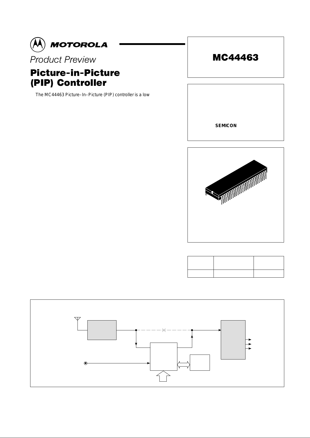
B SUFFIX
PLASTIC PACKAGE
CASE 859
(SDIP)
56
1
Order this document from Analog Marketing
Device
Operating
Temperature Range
Package
ORDERING INFORMATION
MC44463B TJ = –65° to +150°C SDIP
1
MOTOROLA ANALOG IC DEVICE DATA
The MC44463 Picture–In–Picture (PIP) controller is a low cost member of
a family of high performance PIP controllers and video processors for
television. It is a follow–up to the MC44461 PIP, in which two additional
modes of operation have been added. A replay mode is provided, which
captures several seconds of the main picture for replay in four different
speeds. The capture time is programmable in four resolutions (ratio of
captured fields to total fields), which trade the number of fields captured to
the length of replay time. The second additional mode provides for multiple
small picture overlays from a second non–synchronized source. The number
of PIP images is 3 for the 1/9 screen area and 4 for the 1/16 screen area.
Like the MC44461 this is NTSC compatible, I2C bus controlled and available
in the 56–pin shrink dip (SDIP) package.
The main features of the MC44463 are:
• Three PIP Functional Modes: Standard Single Active PIP Mode, Up to 8
Seconds of Capture and Replay Mode, and a 3 or 4 Multiple PIP Mode –
Vertical Stacked with 1 Active at Any One Time
• 4 Capture Resolutions – 1 out of 10, 1:8, 1:6, 1:4. 4 Playback Speeds =
1 Times Acquire Speed; 1/2; 1/4; 1/8
• Full 2 Frame Store for the Single PIP Removes the Rolling
Store/Playback Memory Interference – “Joint Line”
• External Memory for Replay and Multiple Modes: 4 Meg and 16 Meg
• Two NTSC CVBS Inputs – Switchable Main and PIP Video Signals
• Single NTSC CVBS Output Allows Simple TV Chassis Integration
• Two PIP Sizes; 1/16 and 1/9 Screen Area – Freeze Field Feature
• Variable PIP Position in 64–X by 64–Y Steps
• PIP Border with Programmable Color
• Programmable PIP Tint and Saturation Control
• Automatic Main to PIP Contrast Balance
• Vertical Filter
• I
2
C Bus Control – No External Variable Adjustments Needed
• Operates from a Single 5.0 V Supply
• Economical 56–Pin Shrink DIP Package
Composite Video Simplified System Diagram
Video
Processor
CV
1
PIP
MC44463
IIC
Tuner/IF
Back Panel
Composite
Video Input
R
G
B
CV
2
CV CV
in
4
Meg
Memory
This document contains information on a product under development. Motorola reserves the
right to change or discontinue this product without notice.
Motorola, Inc. 1996 Issue 1
Page 2
MC44463
2
MOTOROLA ANALOG IC DEVICE DATA
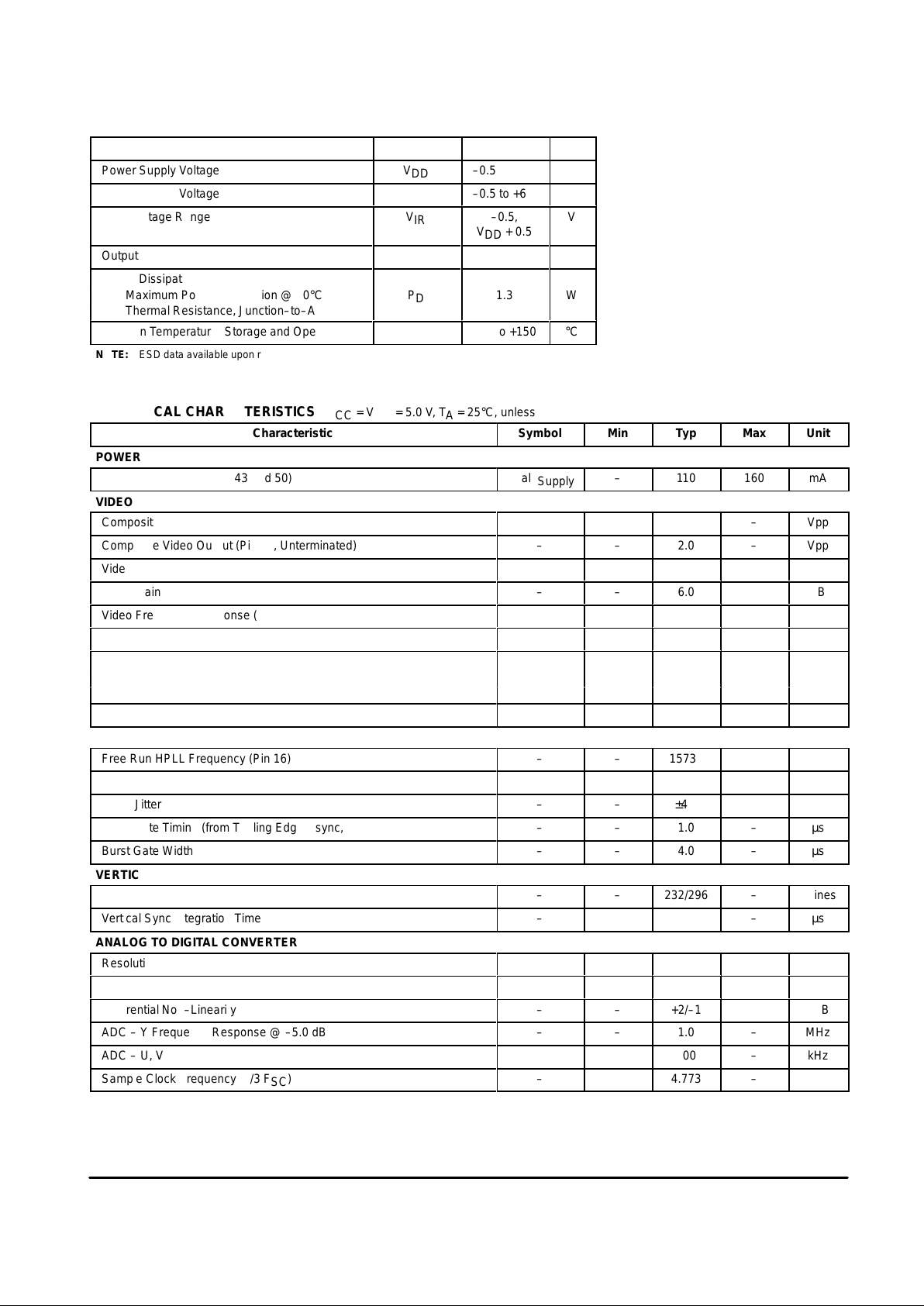
MAXIMUM RATINGS
Rating Symbol Value Unit
Power Supply Voltage
V
DD
–0.5 to +6.0
V
Power Supply Voltage
V
CC
–0.5 to +6.0
V
ББББББББББББ
Á
Input Voltage Range
ÁÁ
Á
V
IR
ÁÁÁ
Á
–0.5,
V
DD
+ 0.5
Á
Á
V
Output Current
I
O
160
mA
Power Dissipation
Maximum Power Dissipation @ 70°C
P
D
1.3
W
Thermal Resistance, Junction–to–Air
R
θJA
59
°C/W
Junction T emperature (Storage and Operating)
T
J
–65 to +150
°C
NOTE: ESD data available upon request.
ELECTRICAL CHARACTERISTICS (V
CC
= VDD = 5.0 V , TA = 25°C, unless otherwise noted.)
Characteristic
Symbol Min Typ Max Unit
POWER SUPPLY
Total Supply (Pins 8, 15, 43 and 50)
Total I
Supply
–
110
160
ÁÁÁ
mA
VIDEO
Composite Video Input (Pin 34 or 36)
CVi
–
1.0
–
ÁÁÁ
Vpp
Composite Video Output (Pin 49, Unterminated)
–
–
2.0
–
ÁÁÁ
Vpp
Video Output DC Level (Sync Tip)
–
–
1.0
–
ÁÁÁ
Vdc
Video Gain
–
–
6.0
–
ÁÁÁ
dB
Video Frequency Response (Main Video to –1.0 dB)
–
–
10
–
ÁÁÁ
MHz
Color Bar Accuracy
–
–
±4.0
–
ÁÁÁ
deg
Video Crosstalk (@ 75% Color Bars)
–
ÁÁÁ
dB
Main to PIP
–
55
–
ÁÁÁ
PIP to Main
–
55
–
БББББББББББББББББ
Output Impedance
ÁÁÁ–ÁÁ–ÁÁ
5.0
ÁÁ
–
ÁÁÁ
ÁÁ
Ω
HORIZONTAL TIMEBASE
Free Run HPLL Frequency (Pin 16)
–
–
15734
–
ÁÁÁ
Hz
HPLL Pull–In Range
–
–
±400
–
ÁÁÁ
Hz
HPLL Jitter
–
–
±4.0
–
ÁÁÁ
ns
Burst Gate Timing (from Trailing Edge Hsync, Pin 24)
–
–
1.0
–
ÁÁÁ
µs
Burst Gate Width
–
–
4.0
–
ÁÁÁ
µs
VERTICAL TIMEBASE
Vertical Countdown Window
–
–
232/296
–
ÁÁÁ
H lines
Vertical Sync Integration T ime
–
–
31
–
ÁÁÁ
µs
ANALOG TO DIGITAL CONVERTER
Resolution
–
–
–
6
ÁÁÁ
Bits
Integral Non–Linearity
–
–
±1
–
ÁÁÁ
LSB
Differential Non–Linearity
–
–
+2/–1
–
ÁÁÁ
LSB
ADC – Y Frequency Response @ –5.0 dB
–
–
1.0
–
ÁÁÁ
MHz
ADC – U, V Frequency Response @ –5.0 dB
–
–
200
–
ÁÁÁ
kHz
Sample Clock Frequency (4/3 FSC)
–
–
4.773
–
ÁÁÁ
MHz
Page 3
MC44463
3
MOTOROLA ANALOG IC DEVICE DATA
ELECTRICAL CHARACTERISTICS (continued) (V
CC
= VDD = 5.0 V , TA = 25°C, unless otherwise noted.)
Characteristic UnitMaxTypMinSymbol
DIGITAL TO ANALOG CONVERTER
Resolution
–
–
–
6
ÁÁÁ
Bits
Integral Non–Linearity
–
–
±1
–
ÁÁÁ
LSB
Differential Non–Linearity
–
–
+2/–1
–
ÁÁÁ
LSB
Tint DAC Control Range (in 64 Steps)
–
–
±10
–
ÁÁÁ
Deg
Saturation DAC Control Range (in 64 steps)
–
–
±6.0
–
ÁÁÁ
dB
NTSC DECODER
Color Kill Threshold
–
–
–24/–16
–
ÁÁÁ
dB
Threshold Hysteresis
–
–
±1.0
–
ÁÁÁ
dB
ACC (Chroma Amplitude Change, +3.0 dB to –12 dB)
–
–
±5.0
–
ÁÁÁ
dB
PIP CHARACTERISTICS
PIP Size
–
ÁÁÁ
1/9 Screen Horizontal
–
114
–
ÁÁÁ
pels
1/9 Screen Vertical
–
71
–
ÁÁÁ
lines
1/16 Screen Horizontal
–
84
–
ÁÁÁ
pels
1/16 Screen Vertical
–
53
–
ÁÁÁ
lines
Border Size Horizontal
–
–
3
–
ÁÁÁ
pels
Border Size Vertical
–
–
2
–
ÁÁÁ
lines
Output PEL Clock (4 FSC)
–
–
14.318
–
ÁÁÁ
MHz
Position Control Range Horizontal (% of Main Picture), 64 Steps
–
–
100
–
ÁÁÁ
%
Position Control Range Vertical (% of Main Picture), 64 Steps
–
–
100
–
ÁÁÁ
%
Figure 1. Representative Block Diagram
This device contains approximately 300,000 active transistors.
Y
V
U
YUV
Clamp
Input
Switch
Low Pass
Filter
Band Pass
Filter
NTSC
Decoder
PIP
Switch
4X S/C
Osc + PLL
16X S/C
Osc + PLL
YUV
Clamp
NTSC
Encoder
4X S/C
Osc + PLL
Filter
Tracking
6–Bit
ADC
H and V
Timebase
Digital
Logic
Tint DAC
Sat DAC
V DAC
Y DAC
3.0 MHz
LPF
3.0 MHz
LPF
3.0 MHz
LPF
33
Y
V
U
40 41 42 51
28
31
1
2
3
4
5
30
5453524746
6
6
6
6
6
3
6
Vert
57.28 MHz
90
°
0
°
14.32 MHz
90
°
0
°
36
34
37
49
38
39
7
44
45
Multiplexer
Video 1
Video 2
Decoder ACC
Main Out
Decoder Xtal
Decoder PLL
16 FSC PLL
Encoder Phase
Encoder ACC
Sync Sep
H PLL
H
in
V
in
SCL
SDA
Reset
Multi T est
Encoder Clamp Caps
Encoder
Xtal
Encoder
PLL
Decoder Clamp Caps
ADC Mid–RefFilter PLL
U DAC
Memory
Control
Logic
6
T est Clock
10 to 27
Memory
Page 4

MC44463
4
MOTOROLA ANALOG IC DEVICE DATA
A0
Figure 2. Application Circuit
X1 – 503 kHz – Murata Erie CSB503F2 or equivalent
X2 – 14.31818 MHz – Fox 143–20 or equivalent
X3 – 14.31818 MHz – Fox 143–20 or equivalent
MCM54400A–C
0.01
40
39
38
37
36
35
34
33
46
45
44
43
42
41
32
31
30
29
48
47
56
55
54
53
52
51
50
49
1
2
3
4
5
6
9
10
11
12
13
14
15
16
7
8
17
18
19
20
21
22
23
24
25
26
27
28
RASB
A9
A0
A1
A2
A3
A4
A5
VSS (dig)
OEB
CASB
DQ2
DQ3
DQ0
DQ1
RWB
H
in
V
in
SCL
SDA
Reset
Test Clock
16 FSC Filter
VDD (dig)
A6
A7
A8
Sync Sep
Decoder PLL
Decoder Y Cap
Decoder Xtal
Decoder ACC
Video In 1
Analog Gnd
Video In 2
Filter PLL
Analog Gnd
Encoder Xtal
Encoder PLL
Encoder ACC
Encoder Phase
Analog V
CC
Decoder V Cap
Decoder U Cap
N/C
N/C
Encoder V Cap
Encoder U Cap
Endoder Y Cap
ADC Mid Ref
Video Out V
CC
Video Out
503 kHz Resonator
H PLL
Multi Test
Sync In
0.01
0.01
0.01
0.1
0.1
0.01
0.01
0.01
0.01
1000
100 k
75
X3
12
5.0 V
Video Out
5.0 V
2700
0.068
68 k
0.22
0.1
0.1
Video 1
Video 2
75 75
0.01
0.01
2.2 k
4.7
µ
F
1001000
100
2.2 µF
470 k
Horiz In
Vert In
I2C Ser Cl
I2C Ser Data
5.0 V
MC44463
5.0 V
0.1 µF
X2
12
47 k
1.0 k
1.0 k
1.0 k
1.0 k
5.0 V 5.0 V
X1
1000
4.7
µ
F330
62 k
2200
12
11
20
19
18
17
16
15
14
13
1
2
3
4
5
6
9
10
7
8
RASN
A9
GN
CASN
DQ2
DQ3
Y
SS
DQ0
DQ1
WN
A1
A0
A8
A7
A6
A5
A4
V
CC
A3
A2
5.0 V
A0
A1
A2
A3
A4
A5
A6
A7
A8
A8
A7
A6
A5
A4
A3
A2
A1
Page 5

MC44463
5
MOTOROLA ANALOG IC DEVICE DATA
I2C REGISTER DESCRIPTIONS
Base write address = 26h
Base read address = 27h
Read Register
There are two active bits in the single read byte available
from the MC44463 as follows:
Write Vertical Indicator (WVI0) – D7
When 0 indicates that the write operation specified by the
last I2C command has been completed.
PIP Sync Detect Bit (PSD0) – D1
When 0 indicates that the PIP video H pulses are present
and the horizontal timebase oscillator is within acceptable
limits.
Write Registers
Read Start Position/Write Start Position Registers
Sub–address = 00h
Write Raster Position Start Bits (WPS0–2) – D0–D2
Establishes the horizontal beginning of the PIP and its
black level measurement gate. This beginning may be varied
by approximately 3.0 µs. The position of this pulse may be
observed through the Multi Test Pin 30 (See Test Mode
Register Sub–address 03h).
Read Raster Position Bits (RPS0–3) – D4–D7
Establishes the clamp gate position for the black level
reference for the main picture. This position may be varied by
approximately 5.0 µs. The position of this pulse may be
observed through the Multi Test Pin 30 (See Test Mode
Register Sub–address 03h).
Pip Switch Delay/Vertical Filter Register
Sub–address = 01h
PIP Switch Delay Bits (PSD0–3) – D0–D3
Delays the start of PIP on time relative to the PIP picture.
These bits are used to center the PIP border and PIP picture
in the horizontal direction.
Vertical Filter Bit (VFON) – D4
When the filter is activated (VFON = 1) a three line
weighted average is taken to provide the data stored in the
field memory.
Border Color Register
Sub–address = 02h
Border Color Bits (BC0–2) – D0–D2
These Bits control the color of the border. Note that when
using one of the saturated border colors it is possible to get
objectionable dot crawl at the edge of the border in some TVs
unless appropriate comb filtering is used in the TV circuitry.
BC (2:0)
Border Color
000
Black
001
White 70%
010
No Border (clear)
011
No Border (clear)
100
Blue
101
Green
110
Red
111
White
Test Mode/Main Vertical and Horizontal Polarity Register
Sub–address = 03h
Internal Test Mode Register (ITM0–2) – D0–D2
Sets the Multi Test Pin output to provide one of several
internal signals for test and production alignment. Also
controls the test memory address counter.
ББББББ
ITM (2:0)
Multi–Test I/O and Function
ББББББ
000
Input – Analog Test mode
ББББББ
001
Input – Digital Test mode
ББББББ
010
Output – Sync Detect
ББББББ
011
Output – PIP Switch
ББББББ
100
Output – PIP H Detect
ББББББ
101
Output – PIP V Detect
ББББББ
110
Output – PIP Clamp
ББББББ
111
Output – Main Clamp
Main vertical polarity select bit (MVP0) – D6
Selects polarity of active level of vertical reference input.
0 = positive going, 1 = negative going.
Main horizontal polarity select bit (MHP0) – D7
Selects polarity of active level of horizontal reference
input. 0 = positive going, 1 = negative going.
PIP Freeze/PIP Size/Main and PIP Video Source Register
Sub–address = 04h
LIVE PIP Select Bits (LIVE_P0–1) – D0–D1
Selects which of the mutliple PIP pictures is the active
“live” one.
ÁÁÁÁ
ÁÁÁ
Á
LIVE_P (1:0)
БББББ
Á
1/16 Size
БББББ
Á
1/9 Size
ÁÁÁÁ
ÁÁÁ
Á
00
БББББ
Á
Top = LIVE
БББББ
Á
Top = LIVE
ÁÁÁÁ
ÁÁÁ
Á
01
БББББ
Á
2nd from Top = LIVE
БББББ
Á
2nd from Top = LIVE
ÁÁÁÁ
ÁÁÁ
Á
10
БББББ
Á
3rd from Top = LIVE
БББББ
Á
3rd from Top = LIVE
ÁÁÁÁ
ÁÁÁ
Á
11
БББББ
Á
4th from Top = LIVE
БББББ
Á
3rd from Top = LIVE
PIP Freeze Bit (STIL0) – D4
When set to one, the most recently received field is
continuously displayed until the freeze bit is cleared.
PIP Size Bit (PSI90) – D5
Switches the PIP size between 1/16 main size (when 0)
and 1/9 main size (when 1).
Main Video Source Select Bit (MSEL0) – D6
Selects which video input will be applied to the PIP switch
as the main video out.
PIP Video Source Select Bit (PSEL0) – D7
Selects which video input will be applied to the video
decoder to provide the PIP video.
ББББББ
MSEL/PSEL
Function
ББББББ
0
Video 1 Input to Main/
Video 1 Input to PIP
ББББББ
БББББ
Á
1
БББББББББ
Á
Video 2 Input to Main/
Video 2 Input to PIP
Page 6

MC44463
6
MOTOROLA ANALOG IC DEVICE DATA
PIP On/PIP Blank Register
Sub–address = 05h
PIP On Bits (PON0–3) – D4–D3
When on (1) turns the corresponding PIP display on.
PON (3:0)
1/16 Size
1/9 Size
0000
No PIP
No PIP
0001
Top = On
Top = On
0010
2nd from Top = On
2nd from Top = On
0100
3rd from Top = On
3rd from Top = On
1000
4th from Top = On
3rd from Top = On
PIP Blanking Bits (PBL0–3) – D4–D7
When on (1) sets the corresponding PIP to black. If the
individual PIP is off, then it will be black when it is turned on.
PBL (7:4)
Function
0000
PIP Picture Normal
0001
Top = Blanked (Set to Black)
0010
2nd from Top = Blanked (Set to Black)
0100
3rd from Top = Blanked (Set to Black)
1000
4th from Top = Blanked (Set to Black)
PIP X Position Register
Sub–address = 06h
X Position Bits (XPS0–5) – D0–D5
Moves the PIP start position from the left to the right
edge of the display in 64 steps. There is protection circuitry
to prevent the PIP from interfering with the main picture
sync pulses.
PIP Y Position Register
Sub–address = 07h
Y Position Bits (YPS0–5) – D0–D5
Moves the PIP start position from the top to the bottom
edge of the display in 64 steps. There is protection circuitry to
prevent the PIP from interfering with the main picture sync
pulses.
PIP Chroma Level Register
Sub–address = 08h
Chroma (C0–5) – D0–D5
The color of the PIP can be adjusted to suit viewer
preference by setting the value stored in these bits. A total of
64 steps varies the color from no color to maximum. This
control acts in conjunction with the auto phase control.
PIP Tint Level Register
Sub–address = 09h
Tint (T0–5) – D0–D5
An auto phase control compares the main color burst to
the internally generated pseudo color burst so that the tints
are matched. In addition to this, the tint of the PIP can be
varied ±10° in a total of 64 steps by changing the value of
these bits to suit viewer preference.
PIP Luma Delay Register
Sub–address = 0Ah
Y Delay (YDL0–2) – D0–D2
Since the Chroma passes through a bandpass filter and
the color decoder, it is delayed with respect to the Luma
signal. Therefore, to time match the Luma and Chroma these
bits are set to a single value determined to be correct in the
application.
PIP Acquire/Playback Register
Sub–address = 0Bh
PIP Acquire Speed Bits (ACQ_SP0–1) – D0–D1
These select the speed of the video acquisition. This is
only active when RE_AQ = 1.
ББББББ
ACQ_SP (1:0)
Function
ББББББ
00
Acquire 1 Out of Every 4 Fields
ББББББ
01
Acquire 1 Out of Every 6 Fields
ББББББ
10
Acquire 1 Out of Every 8 Fields
ББББББ
11
Acquire 1 Out of Every 10 Fields
PIP Save/Clear Bit (RE_AQ) –D2
This bit controls the save and clear function for the instant
replay . The bit value 1 is only effective when PON0–3 = 0000.
(No PIP display.)
ББББББ
RE_AQ (2:2)
Function
ББББББ
0
Save Memory
ББББББ
1
Clear Reacquire
PIP Playback Speed Bits (PB_SP0–1) – D4–D5
These bits control the relative playback speed, to the
acquired speed.
ББББББ
БББББ
Á
PB_SP (5:4)
БББББББББ
Á
Function
ББББББ
БББББ
Á
00
БББББББББ
Á
Playback at 1 x ACQ_SP Speed
ББББББ
БББББ
Á
01
БББББББББ
Á
Playback at 1/2 x ACQ_SP Speed
ББББББ
БББББ
Á
10
БББББББББ
Á
Playback at 1/4 x ACQ_SP Speed
ББББББ
БББББ
Á
11
БББББББББ
Á
Playback at 1/8 x ACQ_SP Speed
PIP Playback Control Bit (PB) – D6
This bit controls the start/stop of the instant replay
function.
ББББББ
PB (6:6)
Function
ББББББ
0
No Action
ББББББ
1
Instant Replay Activated
PIP Fill/Background/Free Run/Test Register
Sub–address = 0Ch
PIP Fill Bits (PIPFILL0–1) – D0–D1
May be used to fill the PIP with one of three selectable
solid colors
ББББББ
PIPFILL (1:0)
Function
ББББББ
00
Normal
ББББББ
01
Red
ББББББ
10
Green
ББББББ
11
Blue
Test Register Bits (INTC0 and MACR0) – D6–D7
When the FRUN is set to 1 the circuitry provides a
generated sync and displays a flat field that can be either
dark blue or gray determined by the BGND bit.
ББББББ
БББББ
Á
BGND (2:2)
БББББББББ
Á
Function
ББББББ
БББББ
Á
0
БББББББББ
Á
Blue
ББББББ
БББББ1БББББББББ
50% White
Page 7

MC44463
7
MOTOROLA ANALOG IC DEVICE DATA
I2C REGISTER TABLE
–
Data Bit
Sub
–
address
D7
D6
D5
D4
D3
D2
D1
D0
00
RPS3
RPS2
RPS1
RPS0
–
WPS2
WPS1
WPS0
01
–
–
–
VFON
PSD3
PSD2
PSD1
PSD0
02
–
–
–
–
–
BC2
BC1
BC0
03
MHP0
MVP0
–
–
–
ITM2
ITM1
ITM0
04
PSEL0
MSEL0
PSI90
STIL0
–
–
LIVE_P1
LIVE_P0
05
PBL3
PBL2
PBL1
PBL0
PON3
PON2
PON1
PON0
06
–
–
XPS5
XPS4
XPS3
XPS2
XPS1
XPS0
07
–
–
YPS5
YPS4
YPS3
YPS2
YPS1
YPS0
08
–
–
C5
C4
C3
C2
C1
C0
09
–
–
T5
T4
T3
T2
T1
T0
0A
–
–
–
–
–
YDL2
YDL1
YDL0
0B
–
PB
PB_SP1
PB_SP0
–
RE_AQ
ACQ_SP1
ACQ_SP0
0C
INTC
MACR
FRUN
–
–
BGND
PIPFILL1
PIPFILL0
Function Control of the MC44463
There are three modes of operation; Single PIP, Multiple
PIP and Replay. These are enabled by setting specific
register bits in the I2C register set.
Single PIP (SPIP) Operation
Register 0Bh : D6 –> 0
Register 05h : D0–D7 –> 01h
Multiple PIP (MPIP) Operation
Register 05h : D0–D3 –> 07h or 0Fh
Register 04h : D0–D1 –> 0 to 3
Register 0Bh : D6 –> 0
Register 0Ch : D5 –> 1, D2 –> 0 or 1 (Optional)
Replay PIP (RPIP) Operation
In sequence, the Capture Ready mode must be first
activated, allowing up to 8 seconds of fill memory with the
desired video stream. Then the Capture mode must be set,
disabling further write to memory. The Capture data may be
re–displayed at any time afterword.
Capture Ready
Register 05h : D0–D3 –> 0
Register 0Bh : D6 –> 0, D2 –> 1, D0–D1 –> 0 to 3
Capture
Register 0Bh : D6 –> 1, D2 –> 0, D4–D5 –> 0 to 3
Register 05h: D0 –> 1
Page 8

MC44463
8
MOTOROLA ANALOG IC DEVICE DATA
B SUFFIX
PLASTIC PACKAGE
CASE 859–01
(SDIP)
ISSUE O
OUTLINE DIMENSIONS
51.69
13.72
3.94
0.36
0.81
0.20
2.92
0
°
0.51
52.45
14.22
5.08
0.56
1.17
0.38
3.43
15
°
1.02
MILLIMETERS
2.035
0.540
0.155
0.014
0.032
0.008
0.115
0
°
0.020
2.065
0.560
0.200
0.022
0.046
0.015
0.135
15
°
0.040
-T-
SEATING
PLANE
C
D
56 PL
E
F
J
56 PL
K
M
G
N
128
56 29
NOTES:
1. DIMENSIONS AND TOLERANCING PER ANSI
Y14.5M, 1982.
2. CONTROLLING DIMENSION: INCH.
3. DIMENSION L TO CENTER OF LEAD WHEN
FORMED PARALLEL.
4. DIMENSIONS A AND B DO NOT INCLUDE MOLD
FLASH. MAXIMUM MOLD FLASH 0.25 (0.010).
MIN MINMAX MAX
INCHES
DIM
A
B
C
D
E
F
G
H
J
K
L
M
N
15.24 BSC0.600 BSC
1.778 BSC
7.62 BSC
0.070 BSC
0.300 BSC
0.89 BSC0.035 BSC
L
H
-A-
-B-
0.25 (0.010) T A
M
S
0.25 (0.010) T B
M
S
Motorola reserves the right to make changes without further notice to any products herein. Motorola makes no warranty, representation or guarantee regarding
the suitability of its products for any particular purpose, nor does Motorola assume any liability arising out of the application or use of any product or circuit, and
specifically disclaims any and all liability, including without limitation consequential or incidental damages. “T ypical” parameters which may be provided in Motorola
data sheets and/or specifications can and do vary in different applications and actual performance may vary over time. All operating parameters, including “Typicals”
must be validated for each customer application by customer’s technical experts. Motorola does not convey any license under its patent rights nor the rights of
others. Motorola products are not designed, intended, or authorized for use as components in systems intended for surgical implant into the body, or other
applications intended to support or sustain life, or for any other application in which the failure of the Motorola product could create a situation where personal injury
or death may occur. Should Buyer purchase or use Motorola products for any such unintended or unauthorized application, Buyer shall indemnify and hold Motorola
and its officers, employees, subsidiaries, affiliates, and distributors harmless against all claims, costs, damages, and expenses, and reasonable attorney fees
arising out of, directly or indirectly, any claim of personal injury or death associated with such unintended or unauthorized use, even if such claim alleges that
Motorola was negligent regarding the design or manufacture of the part. Motorola and are registered trademarks of Motorola, Inc. Motorola, Inc. is an Equal
Opportunity/Affirmative Action Employer.
How to reach us:
USA/EUROPE/Locations Not Listed: Motorola Literature Distribution; JAP AN: Nippon Motorola Ltd.; Tatsumi–SPD–JLDC, 6F Seibu–Butsuryu–Center,
P.O. Box 20912; Phoenix, Arizona 85036. 1–800–441–2447 or 602–303–5454 3–14–2 Tatsumi Koto–Ku, T okyo 135, Japan. 03–81–3521–8315
MFAX: RMF AX0@email.sps.mot.com – TOUCHT ONE 602–244–6609 ASIA/PACIFIC: Motorola Semiconductors H.K. Ltd.; 8B Tai Ping Industrial Park,
INTERNET: http://Design–NET .com 51 Ting Ko k Road, Tai Po, N.T., Hong Kong. 852–26629298
MC44463/D
*MC44463/D*
◊
 Loading...