

Page 1
SEMICONDUCTOR
TECHNICAL DATA
PICTURE–IN–PICTURE
(PIP) CONTROLLER
B SUFFIX
PLASTIC PACKAGE
CASE 859
(SDIP)
56
1
Order this document by MC44460/D
Device
Operating
Temperature Range
Package
ORDERING INFORMATION
MC44460B TJ = –65° to +150°C SDIP
1
MOTOROLA ANALOG IC DEVICE DATA
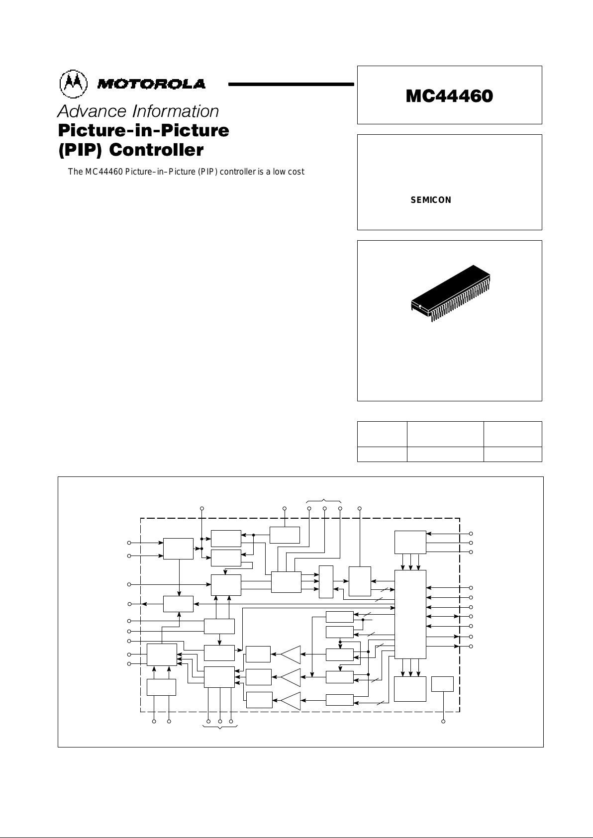
The MC44460 Picture–in–Picture (PIP) controller is a low cost member of
a family of high performance PIP controllers and video signal processors for
television. It is NTSC compatible and contains all the analog signal
processing, control logic and memory necessary to provide for the overlay of
a small picture from a second non synchronized source onto the main picture
of a television. All control and setup of the MC44460 is via a standard two pin
I2C bus interface. The device is fabricated using BICMOS technology. It is
available in a 56–pin shrink dip (SDIP) package.
The main features of the MC44460 are:
• Two NTSC CVBS Inputs
• Switchable Main and PIP Video Signals
• Single NTSC CVBS Output Allows Simple TV Chassis Integration
• Two PIP Sizes; 1/16 and 1/9 Screen Area
• Freeze Field Feature
• Variable PIP Position in 64–X by 64–Y Steps
• PIP Border with Programmable Color
• Programmable PIP Tint and Saturation Control
• Automatic Main to PIP Contrast Balance
• Vertical Filter
• Integrated 64 k Bit DRAM Memory Resulting in Minimal RFI
• Minimal RFI Allows Simple Low Cost Application into TV
• I
2
C Bus Control – No External Variable Adjustments Needed
• Operates from a Single 5.0 V Supply
• Economical 56–Pin Shrink DIP Package
Representative Block Diagram
This device contains 500,000 active transistors.
Y
V
U
Y U V
Clamp
Input
Switch
Low Pass
Filter
Band Pass
Filter
NTSC
Decoder
PIP
Switch
4X S/C
Osc + PLL
16X S/C
Osc + PLL
Y U V
Clamp
NTSC
Encoder
4X S/C
Osc + PLL
Filter
Tracking
6–Bit
ADC
H and V
Timebase
Digital
Logic
I Ref
Memory
8.0 k x 8
DRAM
Tint DAC
Sat DAC
V DAC
Y DAC
3.0 MHz
LPF
3.0 MHz
LPF
3.0 MHz
LPF
33
Y
V
U
40 41 42 51
29
31
32
1
2
3
4
5
10
30
65453524746
6
6
6
6
6
3
6
Vert
57.28 MHz
90
°
0
°
14.32 MHz
90
°
0
°
36
34
37
49
38
39
7
44
45
Multiplexer
Video 1
Video 2
Decoder ACC
Main Out
Decoder Xtal
Decoder PLL
16 FSC PLL
Encoder Phase
Encoder ACC
Sync In
H PLL
503 kHz Res
H
in
V
in
SCL
SDA
Reset
Vid 1/2 Sel
Multi Test
Encoder Clamp Caps
Encoder
Xtal
Encoder
PLL
Cur Ref
Decoder Clamp Caps
ADC Mid–RefFilter PLL
U DAC
28
Sync Out
This document contains information on a new product. Specifications and information herein
are subject to change without notice.
Motorola, Inc. 1996
Page 2
MC44460
2
MOTOROLA ANALOG IC DEVICE DATA
(Top View)
PIN CONNECTIONS
40
39
38
37
36
35
34
33
46
45
44
43
42
41
32
31
30
29
48
47
56
55
54
53
52
51
50
49
1
2
3
4
5
6
9
10
11
12
13
14
15
16
7
8
17
18
19
20
21
22
23
24
25
26
27
28
Decoder PLL
N/C
N/C
N/C
N/C
N/C
N/C
N/C
N/C
Decoder Y Cap
Decoder Xtal
Decoder ACC
Video In 1
Analog Gnd
Video In 2
Filter PLL
VSS (dig)
Video 1/2 Select
N/C
N/C
N/C
VDD (mem)
VSS (mem)
N/C
Analog Gnd
Encoder Xtal
Encoder PLL
Encoder ACC
Encoder Phase
Analog V
CC
Decoder V Cap
Decoder U Cap
H
in
V
in
SCL
SDA
Reset
I
ref
16 FSC Filter
VDD (dig)
N/C
N/C
Encoder V Cap
Encoder U Cap
Endoder Y Cap
ADC Mid Ref
Video Out V
CC
Video Out
N/C
N/C
N/C
Sync Out
503 kHz Resonator
H PLL
Multi Test
Sync In
Page 3
MC44460
3
MOTOROLA ANALOG IC DEVICE DATA
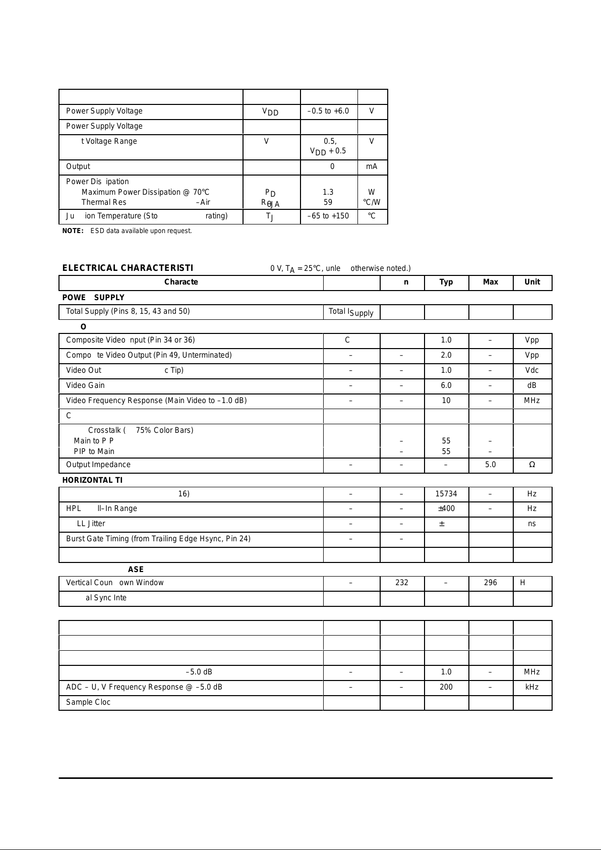
MAXIMUM RATINGS
Rating Symbol Value Unit
Power Supply Voltage
V
DD
–0.5 to +6.0
V
Power Supply Voltage
V
CC
–0.5 to +6.0
V
Input Voltage Range
V
IR
–0.5,
V
DD
+ 0.5
V
Output Current
I
O
160
mA
Power Dissipation
Maximum Power Dissipation @ 70°C
P
D
1.3
W
Thermal Resistance, Junction–to–Air
R
θJA
59
°C/W
Junction Temperature (Storage and Operating)
T
J
–65 to +150
°C
NOTE: ESD data available upon request.
ELECTRICAL CHARACTERISTICS (V
CC
= VDD = 5.0 V, TA = 25°C, unless otherwise noted.)
Characteristic
Symbol Min Typ Max Unit
POWER SUPPLY
Total Supply (Pins 8, 15, 43 and 50)
Total I
Supply
95
124
160
ÁÁÁ
ÁÁÁ
ÁÁÁ
mA
VIDEO
Composite Video Input (Pin 34 or 36)
CVi
–
1.0
–
ÁÁÁ
ÁÁÁ
ÁÁÁ
Vpp
Composite Video Output (Pin 49, Unterminated)
–
–
2.0
–
ÁÁÁ
ÁÁÁ
ÁÁÁ
Vpp
Video Output DC Level (Sync Tip)
–
–
1.0
–
ÁÁÁ
ÁÁÁ
ÁÁÁ
Vdc
Video Gain
–
–
6.0
–
ÁÁÁ
ÁÁÁ
ÁÁÁ
dB
Video Frequency Response (Main Video to –1.0 dB)
–
–
10
–
ÁÁÁ
ÁÁÁ
ÁÁÁ
MHz
Color Bar Accuracy
–
–
±4.0
–
ÁÁÁ
ÁÁÁ
ÁÁÁ
deg
Video Crosstalk (@ 75% Color Bars)
–
ÁÁÁ
ÁÁÁ
ÁÁÁ
dB
Main to PIP
–
55
–
ÁÁÁ
ÁÁÁ
ÁÁÁ
PIP to Main
–
55
–
ÁÁÁ
ÁÁÁ
Output Impedance
–
–
–
5.0
ÁÁÁ
ÁÁÁ
ÁÁÁ
Ω
HORIZONTAL TIMEBASE
Free Run HPLL Frequency (Pin 16)
–
–
15734
–
ÁÁÁ
ÁÁÁ
ÁÁÁ
Hz
HPLL Pull–In Range
–
–
±400
–
ÁÁÁ
ÁÁÁ
ÁÁÁ
Hz
HPLL Jitter
–
–
±4.0
–
ÁÁÁ
ÁÁÁ
ÁÁÁ
ns
Burst Gate Timing (from Trailing Edge Hsync, Pin 24)
–
–
1.0
–
ÁÁÁ
ÁÁÁ
ÁÁÁ
µs
Burst Gate Width
–
–
4.0
–
ÁÁÁ
ÁÁÁ
ÁÁÁ
µs
VERTICAL TIMEBASE
Vertical Countdown Window
–
232
–
296
ÁÁÁ
ÁÁÁ
ÁÁÁ
H lines
Vertical Sync Integration Time
–
–
–
31
ÁÁÁ
ÁÁÁ
ÁÁÁ
µs
ANALOG TO DIGITAL CONVERTER
Resolution
–
–
–
6.0
ÁÁÁ
ÁÁÁ
ÁÁÁ
Bits
Integral Non–Linearity
–
–
±1.0
–
ÁÁÁ
ÁÁÁ
ÁÁÁ
LSB
Differential Non–Linearity
–
–
+2.0/–1.0
–
ÁÁÁ
ÁÁÁ
ÁÁÁ
LSB
ADC – Y Frequency Response @ –5.0 dB
–
–
1.0
–
ÁÁÁ
ÁÁÁ
ÁÁÁ
MHz
ADC – U, V Frequency Response @ –5.0 dB
–
–
200
–
ÁÁÁ
ÁÁÁ
ÁÁÁ
kHz
Sample Clock Frequency (4/3 FSC)
–
–
4.773
–
ÁÁÁ
ÁÁÁ
ÁÁÁ
MHz
Page 4
MC44460
4
MOTOROLA ANALOG IC DEVICE DATA
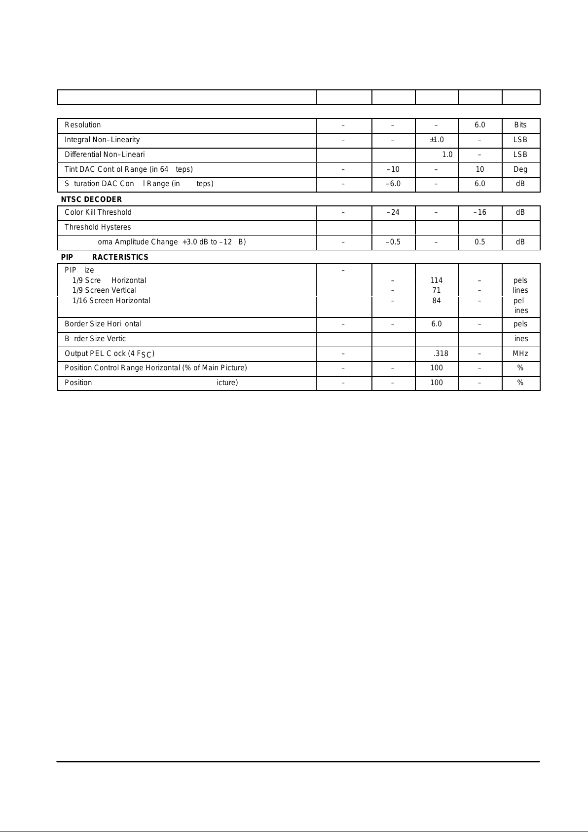
ELECTRICAL CHARACTERISTICS (continued)
(VCC = VDD = 5.0 V, TA = 25°C, unless otherwise noted.)
Characteristic UnitMaxTypMinSymbol
DIGITAL TO ANALOG CONVERTER
Resolution
–
–
–
6.0
ÁÁÁ
ÁÁÁ
ÁÁÁ
Bits
Integral Non–Linearity
–
–
±1.0
–
ÁÁÁ
ÁÁÁ
ÁÁÁ
LSB
Differential Non–Linearity
–
–
+2.0/–1.0
–
ÁÁÁ
ÁÁÁ
ÁÁÁ
LSB
Tint DAC Control Range (in 64 Steps)
–
–10
–
10
ÁÁÁ
ÁÁÁ
ÁÁÁ
Deg
Saturation DAC Control Range (in 64 steps)
–
–6.0
–
6.0
ÁÁÁ
ÁÁÁ
ÁÁÁ
dB
NTSC DECODER
Color Kill Threshold
–
–24
–
–16
ÁÁÁ
ÁÁÁ
ÁÁÁ
dB
Threshold Hysteresis
–
2.0
3.0
4.0
ÁÁÁ
ÁÁÁ
ÁÁÁ
dB
ACC (Chroma Amplitude Change, +3.0 dB to –12 dB)
–
–0.5
–
0.5
ÁÁÁ
ÁÁÁ
ÁÁÁ
dB
PIP CHARACTERISTICS
PIP Size
–
ÁÁÁ
ÁÁÁ
ÁÁÁ
1/9 Screen Horizontal
–
114
–
ÁÁÁ
ÁÁÁ
ÁÁÁ
pels
1/9 Screen Vertical
–
71
–
ÁÁÁ
ÁÁÁ
lines
1/16 Screen Horizontal
–
84
–
ÁÁÁ
ÁÁÁ
ÁÁÁ
pels
1/16 Screen Vertical
–
54
–
ÁÁÁ
ÁÁÁ
ÁÁÁ
lines
Border Size Horizontal
–
–
6.0
–
ÁÁÁ
ÁÁÁ
ÁÁÁ
pels
Border Size Vertical
–
–
2.0
–
ÁÁÁ
ÁÁÁ
ÁÁÁ
lines
Output PEL Clock (4 FSC)
–
–
14.318
–
ÁÁÁ
ÁÁÁ
ÁÁÁ
MHz
Position Control Range Horizontal (% of Main Picture)
–
–
100
–
ÁÁÁ
ÁÁÁ
ÁÁÁ
%
Position Control Range Vertical (% of Main Picture)
–
–
100
–
ÁÁÁ
ÁÁÁ
ÁÁÁ
%
Page 5
MC44460
5
MOTOROLA ANALOG IC DEVICE DATA
PIN FUNCTION DESCRIPTION
Pin Equivalent Internal Circuit Description
1
БББББББББББББ
БББББББББББББ
БББББББББББББ
БББББББББББББ
БББББББББББББ
БББББББББББББ
БББББББББББББ
БББББББББББББ
1
1.0 k
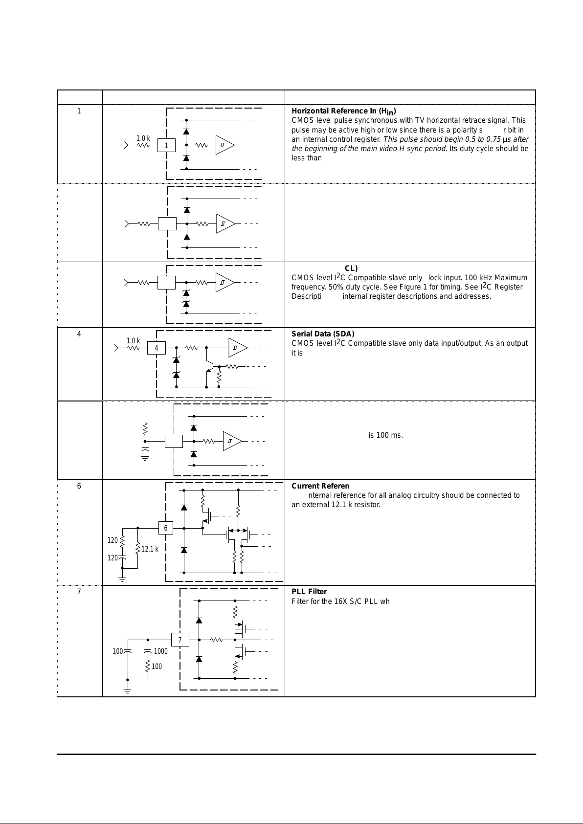
Horizontal Reference In (Hin)
CMOS level pulse synchronous with TV horizontal retrace signal. This
pulse may be active high or low since there is a polarity selector bit in
an internal control register.
This pulse should begin 0.5 to 0.75 µs after
the beginning of the main video H sync period.
Its duty cycle should be
less than 50%.
2
БББББББББББББ
БББББББББББББ
БББББББББББББ
БББББББББББББ
БББББББББББББ
БББББББББББББ
БББББББББББББ
2
1.0 k
Vertical Reference In (Vin)
CMOS level pulse synchronous with TV vertical retrace signal. This
pulse may be active high or low since there is a polarity selector bit in
an internal control register. This pulse should begin during the main
video vertical interval and have a duration of at least .5H.
3
3
1.0 k
Serial Clock (SCL)
CMOS level I2C Compatible slave only clock input. 100 kHz Maximum
frequency. 50% duty cycle. See Figure 1 for timing. See I2C Register
Description for internal register descriptions and addresses.
4
4
1.0 k
Serial Data (SDA)
CMOS level I2C Compatible slave only data input/output. As an output
it is open collector. See Figure 1 for timing. See I2C Register
Description for internal register descriptions and addresses.
5
БББББББББББББ
БББББББББББББ
БББББББББББББ
БББББББББББББ
БББББББББББББ
БББББББББББББ
БББББББББББББ
5
22 k
0.22
5.0
Reset
The active low, Power On Reset initializes all internal registers to zero
and resets the I2C interface. Minimum active low time required for
Power On Reset reset is 100 ms.
6
БББББББББББББ
БББББББББББББ
БББББББББББББ
БББББББББББББ
БББББББББББББ
БББББББББББББ
БББББББББББББ
БББББББББББББ
БББББББББББББ
6
120
12.1 k
120
Current Reference
The internal reference for all analog circuitry should be connected to
an external 12.1 k resistor.
7
БББББББББББББ
БББББББББББББ
БББББББББББББ
БББББББББББББ
БББББББББББББ
БББББББББББББ
БББББББББББББ
БББББББББББББ
БББББББББББББ
БББББББББББББ
7
100 1000
100
PLL Filter
Filter for the 16X S/C PLL which is phase locked to the 4X S/C
oscillator.
Pins 11 to 13, 16 to 27, 55 and 56 are test pins configured as outputs in a high impedance state. In an application, no connection should be made to these pins.
Page 6

MC44460
6
MOTOROLA ANALOG IC DEVICE DATA
PIN FUNCTION DESCRIPTION (continued)
Pin DescriptionEquivalent Internal Circuit
8
14, 43, 50
9
15, 35, 48
БББББББББББББ
БББББББББББББ
БББББББББББББ
БББББББББББББ
БББББББББББББ
БББББББББББББ
БББББББББББББ
БББББББББББББ
БББББББББББББ
БББББББББББББ
БББББББББББББ
БББББББББББББ
9 8 14, 43, 50 15, 35, 48
V
SS
V
DD
M V
DD
An V
CC
Vid V
CC
M V
SS
An Gnd
An Gnd
VDD, V
SS
The four VDD pins must be externally connected to a 5.0 V (±5%)
supply. The four VSS lines must externally connect to their respective
VDD bypass return(s) to ensure that no ground disturbances occur in
operation. All supplies must be properly bypassed and isolated for the
application. Bypass capacitors of 10 µF in parallel with 0.1 µF for each
supply are recommended as a general guideline. The 0.1 µF, high
frequency bypass capacitors should be placed as close to the power
pins as practical.
10
БББББББББББББ
БББББББББББББ
БББББББББББББ
БББББББББББББ
БББББББББББББ
БББББББББББББ
БББББББББББББ
10
Video 1/2 Select Output
High output level indicates that Video 1 is selected to be the main
picture video. Low output level indicates Video 2 is selected to be the
main picture video.
28
БББББББББББББ
БББББББББББББ
БББББББББББББ
БББББББББББББ
БББББББББББББ
БББББББББББББ
БББББББББББББ
БББББББББББББ
БББББББББББББ
28
Sync Out
Outputs the video signal selected as the PIP to be filtered and applied
to the H and V timebase through the Sync In pin.
29
БББББББББББББ
БББББББББББББ
БББББББББББББ
БББББББББББББ
БББББББББББББ
БББББББББББББ
БББББББББББББ
БББББББББББББ
БББББББББББББ
БББББББББББББ
29
Sync In
PIP sync pulses are externally filtered and applied to the H and V
timebase to allow H and V synchronization.
30
БББББББББББББ
БББББББББББББ
БББББББББББББ
БББББББББББББ
БББББББББББББ
БББББББББББББ
БББББББББББББ
30
10 k
Multi Test
Under control of I2C bus output signals for test and adjustment are
provided through this pin.
31
БББББББББББББ
БББББББББББББ
БББББББББББББ
БББББББББББББ
БББББББББББББ
БББББББББББББ
БББББББББББББ
БББББББББББББ
БББББББББББББ
БББББББББББББ
31
0.1 4.7 µF
2.2 k
H PLL
Connection for horizontal timebase PLL filter. See separate discussion
for filter values.
Pins 11 to 13, 16 to 27, 55 and 56 are test pins configured as outputs in a high impedance state. In an application, no connection should be made to these pins.
Page 7

MC44460
7
MOTOROLA ANALOG IC DEVICE DATA
PIN FUNCTION DESCRIPTION (continued)
Pin DescriptionEquivalent Internal Circuit
32
БББББББББББББ
БББББББББББББ
БББББББББББББ
БББББББББББББ
БББББББББББББ
БББББББББББББ
БББББББББББББ
БББББББББББББ
БББББББББББББ
32
503 kHz
1000
503 kHz Resonator
Single pin oscillator is used as the main timebase reference. It is phase
locked to the PIP H sync pulses. This oscillator provides the reference
to the system logic, PIP decoder and vertical timebase circuitry.
33
БББББББББББББ
БББББББББББББ
БББББББББББББ
БББББББББББББ
БББББББББББББ
БББББББББББББ
БББББББББББББ
БББББББББББББ
БББББББББББББ
БББББББББББББ
33
0.1
Filter PLL
The on board reference filter produces a phase shift which is
measured and applied to an internal filter PLL. This capacitor
connected to this pin stores the phase correction voltage for the PLL
which sets the 90° phase correction reference for the rest of the on
chip filters.
36 and 34
БББББББББББББ
БББББББББББББ
БББББББББББББ
БББББББББББББ
БББББББББББББ
БББББББББББББ
БББББББББББББ
БББББББББББББ
БББББББББББББ
БББББББББББББ
19 k
2.0 k
0.1
Composite
Video
R
Video Input 1 and 2
Accepts ac coupled 1.0 Vpp composite video input usually from a
source generated inside the TV and an external video source.
The series coupling capacitor also functions as the storage capacitor
for the clamp voltage for the input circuit. It is necessary to return the
input of this capacitor to ground through a dc low impedance to enable
this clamp function. R = 50 to 100 Ω is acceptable.
37
БББББББББББББ
БББББББББББББ
БББББББББББББ
БББББББББББББ
БББББББББББББ
БББББББББББББ
БББББББББББББ
БББББББББББББ
БББББББББББББ
БББББББББББББ
37
0.22
Decoder ACC
The Decoder ACC pin provides access to the internal chroma decoder
automatic gain control amplifier. The ACC capacitor filters the feedback
loop of this amplifier.
During PIP burst gate time a voltage proportional to the burst gate
magnitude is stored on the capacitor connected to this pin to
compensate for input chroma level variation and provide a constant
U and V output level to the A/D conversion stage.
38
БББББББББББББ
БББББББББББББ
БББББББББББББ
БББББББББББББ
БББББББББББББ
БББББББББББББ
БББББББББББББ
БББББББББББББ
БББББББББББББ
38
14.3 MHz
18
Decoder Crystal
4X Sub–Carrier crystal used to synchronize the decoding of the PIP
UV information prior to A/D conversion, sub–sampling and storage in
the field memory.
The crystal frequency is 14.31818 MHz.
Pins 11 to 13, 16 to 27, 55 and 56 are test pins configured as outputs in a high impedance state. In an application, no connection should be made to these pins.
Page 8

MC44460
8
MOTOROLA ANALOG IC DEVICE DATA
PIN FUNCTION DESCRIPTION (continued)
Pin DescriptionEquivalent Internal Circuit
39
БББББББББББББ
БББББББББББББ
БББББББББББББ
БББББББББББББ
БББББББББББББ
БББББББББББББ
БББББББББББББ
БББББББББББББ
БББББББББББББ
БББББББББББББ
39
2700 0.068
68 k
Decoder PLL
Connection for Decoder PLL filter. See separate discussion for filter
values.
44
БББББББББББББ
БББББББББББББ
БББББББББББББ
БББББББББББББ
БББББББББББББ
БББББББББББББ
БББББББББББББ
БББББББББББББ
БББББББББББББ
2.0 k
0.01
44
Encoder Phase
Phase difference of the main to encoded burst is sampled and applied
to the capacitor connected to this pin to shift the phase of the
re–encoded chrominance to match the main.
45
БББББББББББББ
БББББББББББББ
БББББББББББББ
БББББББББББББ
БББББББББББББ
БББББББББББББ
БББББББББББББ
БББББББББББББ
БББББББББББББ
БББББББББББББ
45
0.01
Encoder ACC
The Encoder ACC pin provides access to the internal chroma
reference sample and hold circuit, which stores the sampled value of
the main channel chroma burst amplitude on this external ACC
capacitor. The ACC amplifier matches the chroma amplitude of the
insert picture to that of the main picture.
46
БББББББББББББ
БББББББББББББ
БББББББББББББ
БББББББББББББ
БББББББББББББ
БББББББББББББ
БББББББББББББ
БББББББББББББ
БББББББББББББ
46
1000 1.0 µF
18 k
Encoder PLL
Connection for Encoder PLL filter. See separate discussion for filter
values.
47
БББББББББББББ
БББББББББББББ
БББББББББББББ
БББББББББББББ
БББББББББББББ
БББББББББББББ
БББББББББББББ
БББББББББББББ
БББББББББББББ
38
14.3 MHz
18
Encoder Crystal
4X Sub–Carrier crystal used to synchronize the encoding of the PIP
YUV from the field memory with the main video. The output from this
PLL is phase corrected to match the PIP video signal to the main video
at the PIP switch.
The crystal frequency is 14.31818 MHz.
Pins 11 to 13, 16 to 27, 55 and 56 are test pins configured as outputs in a high impedance state. In an application, no connection should be made to these pins.
Page 9

MC44460
9
MOTOROLA ANALOG IC DEVICE DATA
PIN FUNCTION DESCRIPTION (continued)
Pin DescriptionEquivalent Internal Circuit
49
БББББББББББББ
БББББББББББББ
БББББББББББББ
БББББББББББББ
БББББББББББББ
БББББББББББББ
БББББББББББББ
БББББББББББББ
БББББББББББББ
4.8 k
49
75
Composite
Video
Video Out
The selected Video 1/2 input is available at the Video Out mixed with
the PIP overlay when selected. This signal is a nominal 2.0 V
peak–to–peak signal unterminated. This connection is intended to
drive an external series 75 Ω load into a 75 Ω termination to ground to
provide a 1.0 Vpp signal at the termination.
51
БББББББББББББ
БББББББББББББ
БББББББББББББ
БББББББББББББ
БББББББББББББ
БББББББББББББ
БББББББББББББ
БББББББББББББ
БББББББББББББ
0.1
51
ADC Mid Reference
The mid–point of the A/D converter reference divider network is
brought out on this pin in order to add a filter capacitor to remove any
noise in the network.
54, 53, 52,
42, 41, 40
БББББББББББББ
БББББББББББББ
БББББББББББББ
БББББББББББББ
БББББББББББББ
БББББББББББББ
БББББББББББББ
БББББББББББББ
БББББББББББББ
45
0.01
Encoder and Decoder YUV Caps
During the internal H rate clamping time the YUV reference levels are
set by the charge on the capacitors attached to these pins. The
nominal value of these capacitors should be 0.01 µF.
Pins 11 to 13, 16 to 27, 55 and 56 are test pins configured as outputs in a high impedance state. In an application, no connection should be made to these pins.
Figure 1. I2C Data Transfer
MSB MSB
ACK ACK
1 2 7 8 9 1 2 7 8 9
S Slave Address R/
W
A Data A Data A P
Data Transferred
(n Bytes + Acknowledge)
A = Acknowledge
S = Start
P = Stop
Start
Condition
Stop
Condition
Page 10

MC44460
10
MOTOROLA ANALOG IC DEVICE DATA
I2C REGISTER DESCRIPTIONS
Base read address = 24h
Base write address = 25h
Read Register
There are two active bits in the single read byte available
from the MC44460 as follows:
Write Vertical Indicator (WVI0) – D7
When 0 indicates that the write operation specified by the
last I2C command has been completed.
PIP Sync Detect Bit (PSD0) – D1
When 0 indicates that the PIP video H pulses are present
and the horizontal timebase oscillator is within acceptable
limits.
Write Registers
Read Start Position/Write Start Position Registers
Sub–address = 00h
Write Raster Position Start Bits (WPS0–2) – D0–D2
Establishes the horizontal beginning of the PIP and its
black level measurement gate. This beginning may be varied
by approximately 3.0 µs. The position of this pulse may be
observed through the Multi Test Pin 30 (See Test Mode
Register Sub–address 03h).
Read Raster Position Bits (RPS0–3) – D4–D7
Establishes the clamp gate position for the black level
reference for the main picture. This position may be varied by
approximately 5.0 µs. The position of this pulse may be
observed through the Multi Test Pin 30 (See Test Mode
Register Sub–address 03h).
Pip Switch Delay/Vertical Filter Register
Sub–address = 01h
PIP Switch Delay Bits (PSD0–3) – D0–D3
Delays the start of PIP on time relative to the PIP picture.
These bits are used to center the PIP border and PIP picture
in the horizontal direction.
Vertical Filter Bit (VFON) – D4
When the filter is activated (VFON = 1) a three line
weighted average is taken to provide the data stored in the
field memory.
Border Color Register
Sub–address = 02h
Border Color Bits (BC0–2) – D0–D2
These Bits control the color of the border. Note that when
using one of the saturated border colors it is possible to get
objectionable dot crawl at the edge of the border in some TVs
unless appropriate comb filtering is used in the TV circuitry.
BC (2:0)
Border Color
000
Black
001
White 70%
010
No Border (clear)
011
No Border (clear)
100
Blue
101
Green
110
Red
111
White
Test Mode/Main Vertical and Horizontal Polarity Register
Sub–address = 03h
Internal Test Mode Register (ITM0–2) – D0–D2
Sets the Multi Test Pin output to provide one of several
internal signals for test and production alignment. Also
controls the test memory address counter.
ББББББ
ББББББ
ББББББ
ITM (2:0)
Multi–Test I/O and Function
ББББББ
ББББББ
ББББББ
000
Input – Analog Test mode
ББББББ
ББББББ
ББББББ
001
Input – Digital Test mode
ББББББ
ББББББ
ББББББ
010
Output – Multi Sync Detect
ББББББ
ББББББ
ББББББ
011
Output – Multi PIP Switch
ББББББ
ББББББ
ББББББ
100
Output – Multi PIP H Detect
ББББББ
ББББББ
ББББББ
101
Output – Multi PIP V Detect
ББББББ
ББББББ
ББББББ
110
Output – Multi PIP Clamp
ББББББ
ББББББ
ББББББ
111
Output – Multi Main Clamp
Main vertical polarity select bit (MVP0) – D6
Selects polarity of active level of vertical reference input.
0 = positive going, 1 = negative going.
Main horizontal polarity select bit (MHP0) – D7
Selects polarity of active level of horizontal reference
input. 0 = positive going, 1 = negative going.
PIP Freeze/PIP Size/Main and PIP Video Source Register
Sub–address = 04h
PIP Freeze Bit (STIL0) – D4
When set to one, the most recently received field is
continuously displayed until the freeze bit is cleared.
PIP Size Bit (PSI90) – D5
Switches the PIP size between 1/16 main size (when 0)
and 1/9 main size (when 1).
Main Video Source Select Bit (MSEL0) – D6
Selects which video input will be applied to the PIP switch
as the main video out.
PIP Video Source Select Bit (PSEL0) – D7
Selects which video input will be applied to the video
decoder to provide the PIP video.
ББББББ
ББББББ
ББББББ
MSEL/PSEL
Function
ББББББ
ББББББ
ББББББ
0
Video 1 Input to Main/
Video 1 Input to PIP
ББББББ
ББББББ
ББББББ
ББББББ
1
Video 2 Input to Main/
Video 2 Input to PIP
PIP On/PIP Blank Register
Sub–address = 05h
PIP On Bit (PON0) – D0
When on (1) turns the PIP on.
PIP Blanking Bit (PBL0) – D4
When on (1) sets the PIP to black. If the PIP is off, then it
will be black if it is turned on. Overrides all other settings of
the PIP control.
PIP X Position Register
Sub–address = 06h
X Position Bits (XPS0–5) – D0–D5
Moves the PIP start p osition from the l eft to the r ight
edge of the display in 64 steps. There is protection circuitry
Page 11

MC44460
11
MOTOROLA ANALOG IC DEVICE DATA
to prevent the P IP from i nterfering with the m ain picture
sync pulses.
PIP Y Position Register
Sub–address = 07h
Y Position Bits (YPS0–5) – D0–D5
Moves the PIP start position from the top to the bottom
edge of the display in 64 steps. There is protection circuitry to
prevent the PIP from interfering with the main picture sync
pulses.
PIP Chroma Level Register
Sub–address = 08h
Chroma (C0–5) – D0–D5
The color of the PIP can be adjusted to suit viewer
preference by setting the value stored in these bits. A total of
64 steps varies the color from no color to maximum. This
control acts in conjunction with the auto phase control.
PIP Tint Level Register
Sub–address = 09h
Tint (T0–5) – D0–D5
An auto phase control compares the main color burst to
the internally generated pseudo color burst so that the tints
are matched. In addition to this, the tint of the PIP can be
varied ±10° in a total of 64 steps by changing the value of
these bits to suit viewer preference.
PIP Luma Delay Register
Sub–address = 0Ah
Y Delay (YDL0–2) – D0–D2
Since the Chroma passes through a bandpass filter and
the color decoder, it is delayed with respect to the Luma
signal. Therefore, to time match the Luma and Chroma these
bits are set to a single value determined to be correct in the
application.
Pip Fill/Test Register
Sub–address = 0Ch
PIP Fill Bits (PIPFILL0–1) – D0–D1
May be used to fill the PIP with one of three selectable
solid colors
Test Register Bits (INTC0 and MACR0) – D6–D7
Used for production test only.
I2C REGISTER TABLE
Data Bit
Sub–
address
D7
D6
D5
D4
D3
D2
D1
D0
00
RPS3
RPS2
RPS1
RPS0
–
WPS2
WPS1
WPS0
01
–
–
–
VFON
PSD3
PSD2
PSD1
PSD0
02
–
–
–
–
–
BC2
BC1
BC0
03
MHP0
MVP0
–
–
–
ITM2
ITM1
ITM0
04
PSEL0
MSEL0
PSI90
STIL0
–
–
–
–
05
–
–
–
PBL0
–
–
–
PON0
06
–
–
XPS5
XPS4
XPS3
XPS2
XPS1
XPS0
07
–
–
YPS5
YPS4
YPS3
YPS2
YPS1
YPS0
08
–
–
C5
C4
C3
C2
C1
C0
09
–
–
T5
T4
T3
T2
T1
T0
0A
–
–
–
–
–
YDL2
YDL1
YDL0
0B
–
–
–
–
–
–
–
–
0C
–
–
–
–
–
–
–
–
Page 12

MC44460
12
MOTOROLA ANALOG IC DEVICE DATA
CIRCUIT DESCRIPTION
The MC44460 Picture–in–Picture (PIP) controller is
composed of an analog section, logic section and an
8.0 k x 8–bit DRAM array. A block diagram showing details of
all of these sections is shown in the Representative Block
Diagram.
The analog section includes an Input Switch, Sync
Processor, Filters, PLLs, NTSC Decoder , ADC, DACs, NTSC
Encoder and Output Switch. All necessary controls are
provided by registers in the logic section. These registers are
set by external control through the I2C Bus.
In operation, the MC44460 overlays a single PIP on the
main video in either a 1/9th or 1/16th size. In 1/9th, the PIP is
152 samples (114 Y, 19 V, 19 U) by 70 lines and occupies
8094 bytes of the 8192 byte DRAM. The 1/16 size is 112
samples (84 Y, 14 V, 14 U) by 52 lines and occupies 4452
bytes of the DRAM. An extra line of data is stored for each
PIP size to allow for interlace disorder correction. The 6:1:1
samples are formatted by the logic section as follows in order
to efficiently utilize memory:
Byte 1: Y0(5:0), V(1:0)
Byte 2: Y1(5:0), V(3:2)
Byte 3: Y2(5:0), V(5:4)
Byte 4: Y3(5:0), U(1:0)
Byte 5: Y4(5:0), U(3:2)
Byte 6: Y5(5:0), U(5:4)
Refer to the block diagram. Both the video inputs are
applied to an input switch which is controlled by the I2C bus
interface. Either of the inputs is applied to the PIP processing
circuitry and either to the main video signal path of the output
switch. The signal applied to the PIP processor also provides
the vertical sync reference to the PIP processor.
The PIP output from the switch is applied to a 1.0 MHz
cutoff low pass GmC biquad filter to extract the luminance
signal and a similar bandpass filter to pass chroma to the
decoder section. These filters are tracked to a master GmC
cell using subcarrier as a reference. A single–ended
transconductance stage with relatively large signal handling
ability (>2.5 Vpp @ 4.5 V VCC) is used to avoid potential
noise problems.
Figure 2. NTSC Decoder
Color
Killer
In
90
°
ACC
Switching
PLL
Filter
XVCO/
Divide
Mult 1 Mult 2
BG H
U V
0
°
The NTSC Decoder (Figure 2) consists of two multipliers,
a voltage controlled 4 X S/C crystal oscillator/divider,
Automatic Color Control (ACC) block, Color Kill circuit and
necessary switching. During Burst Gate time, the ACC block
in the NTSC Decoder is calibrated with respect to burst
magnitude by applying the output of multiplier 1 to the
reference input of the ACC block. The result is U and V
outputs which are 0.6 V ± 0.5 dB for burst amplitudes varying
from –12 dB to 3.0 dB. The second multiplier serves as a
phase detector during color burst to match the 90 degree
output from the XVCO to the 180 degree color burst and feed
a correction current to the PLL filter. The phase is correct
when the two signals are 90 degrees out of phase.
During the H drive time, the output of the multipliers is fed
to the YUV clamp, filtered to 200 KHz and input along with the
Y signal to the multiplexer.
The YUV samples are fed through a multiplexer to a single
six bit A/D converter. The A/D is a flash type architecture and
is capable of digitizing at a 20 MHz sample rate. It is
comprised of an internal bandgap source voltage reference,
a 64 tap resistor ladder comparator array, a binary encoder
and output latches. Once the multiplexer has switched,
sufficient time is provided to allow the A/D converter to settle
before the reading is latched. The encoder code is
determined from the values of any comparators which are not
metastable.
The multiplexer and A/D converter receive and convert the
YUV data at a 4FSC/3 rate for a 1/9th size picture or FSC for
a 1/16th size picture. The samples are taken in the following
way to simplify the control logic:
Y,V,Y,U,Y,V,Y,U
To provide a 6:1:1 format, one of three U and V samples is
saved to memory giving a luminance sample rate of 2FSC/3
for a 1/9th picture and FSC/2 for a 1/16 picture. In the vertical
direction, one line of every 3 (1/9th picture) or 4 (1/16th
picture) are saved. In order to avoid objectionable artifacts, a
piece–wise vertical filter is used to take a weighted average
on the luminance samples. For three lines (1/9th size) the
weight is 1/4 + 1/2 + 1/4 and for four lines (1/16 size) it is
1/4 + 1/4 + 1/4 + 1/4. This filter also delays the luma samples
correcting for the longer chroma signal path through the
decoder.
Finally the logic incorporates a field generator to
determine the current field in order to correct interlace
disorders arising from a single field memory.
A separate process runs in the logic section to create the
PIP window on the main picture. Control signals are
generated and sent to the memory controller to read data
from the field memory. Data from the eight bit memory are
then de–multiplexed into a six bit YUV format, borders are
added, blanking is generated for the video clamps and sent to
the Y, U and V DACs. Since the PIP display is based on a
data clock, it is important to minimize the main display clock
skew on a line by line basis. Skew is minimized in the
MC44460 by reclocking the display timebase to the nearest
rising or falling edge of a 16FSC clock. This produces a
maximum line to line skew of approximately 8.0 ns which is
not perceptible to the viewer. The PIP write logic also
incorporates a field generator for use by the memory
controller for interlace disorder correction. Interlace disorder
can occur when the line order of the two fields of the PIP
image is swapped due to a mismatch with the main picture
field or due to an incomplete field being displayed from
memory. The main and PIP field generators, along with
monitoring, when the PIP read address passes the PIP write
Page 13

MC44460
13
MOTOROLA ANALOG IC DEVICE DATA
address, allows the read address to the memory to be
modified to correct for interlace disorder.
The read logic can provide various border colors: black,
75% white (light gray), 50% white (medium gray), red, green,
blue or transparent (no border). In a system without an
adaptive comb filter, borders which contain no chroma give
the best results. Also built into the read logic is a PIP fill mode
which allows the PIP window to be filled with either a solid
green, blue or red color as an aid in aligning the PIP analog
color circuitry.
Because the DAC output video will be referenced during
back porch time, the read processor zeroes the luminance
value and sets the bipolar U and V values to mid–range
during periods outside the PIP window to ensure clamping at
correct levels. Since the PIP window is positioned relative to
the main picture’s vertical and horizontal sync, a safety
feature turns off the window if the window encroaches upon
the sync period, thus preventing erroneous clamping.
The Y, U and V DACs are all three of the same design. A
binary weighted current source is used, split into two, three
bit levels. In the three most significant bits, the current
sources are cascaded to improve the matching to the three
least significant current sources. Analog transmission gates,
switched by the bi–phase outputs of the data latches, feed
the binary currents to the single ended current mirror. The
output current is subsequently clamped and filtered for
processing buy the NTSC Encoder.
The outputs of the U and V DACS are buffered and burst
flag pulses added to both signals. The U burst flag is fixed to
generate a –180° color burst at the modulator output. The V
burst flag is variable under the control of an internal register
set through the I2C bus to provide a variable tint. Saturation is
controlled by varying a register which sets the reference
voltage to the U and V DACs. This is also under I2C bus
control. By oversampling the U and V DACs, it was possible
to use identical post–DAC filtering for Y, U and V, thereby
reducing the delay inequalities between Y and UV and also
simplifying the design. After filtering, the U and V signals are
clamped to an internal reference voltage during horizontal
blanking periods and fed to the U and V modulators. In the
NTSC Decoder, the Y, U and V signals were scaled to use the
entire A/D range. Gain through the NTSC Encoder is set to
properly match these amplitudes.
The phase of the re–encoded chrominance must match
that of the incoming main video signal at the input to the PIP
switch, so a separate first order PLL is placed within the loop
of the main video signal burst PLL. The first order PLL
compares the phase of the main burst with that of the
encoded burst and moves the oscillator phase so that they
match. A special phase shift circuit allowing a continuous
range of 180° was developed to do this.
The amplitude of the re–encoded chrominance signal
must also match that of the main video signal. To do this, a
synchronous amplitude comparator looks at both burst
signals and adjusts the chrominance amplitude in the
modulator section of the NTSC encoder. The Y signal from
the YDAC is compared to the main video signal at black level
during back porch time and clamped to this same black level
voltage. The PIP chrominance and luminance are then
added together and fed to the PIP output switch through a
buffered output.
Page 14

MC44460
14
MOTOROLA ANALOG IC DEVICE DATA
0.1
Figure 3. Application Circuit
40
39
38
37
36
35
34
33
46
45
44
43
42
41
32
31
30
29
48
47
56
55
54
53
52
51
50
49
1
2
3
4
5
6
9
10
11
12
13
14
15
16
7
8
17
18
19
20
21
22
23
24
25
26
27
28
N/C
N/C
N/C
N/C
N/C
N/C
N/C
N/C
VSS (dig)
Video 1/2 Select
N/C
N/C
N/C
VDD (mem)
VSS (mem)
N/C
H
in
V
in
SCL
SDA
Reset
I
ref
16 FSC Filter
VDD (dig)
N/C
N/C
N/C
Sync Out
Decoder PLL
Decoder Y Cap
Decoder Xtal
Decoder ACC
Video In 1
Analog Gnd
Video In 2
Filter PLL
Analog Gnd
Encoder Xtal
Encoder PLL
Encoder ACC
Encoder Phase
Analog V
CC
Decoder V Cap
Decoder U Cap
N/C
N/C
Encoder V Cap
Encoder U Cap
Endoder Y Cap
ADC Mid Ref
Video Out V
CC
Video Out
503 kHz Resonator
H PLL
Multi Test
Sync In
0.01
0.01
0.01
0.01
1.0
µ
F
0.01
0.01
0.01
0.01
0.01
1000
18 k
75
X3
18
5.0 V
Video Out
5.0 V
2700
0.068
68 k
18
X2
0.22
0.1
0.1
Video 1
Video 2
75 75
1000
0.01
X1
0.1
2.2 k
4.7
µ
F
62 k
4.7 µF
2200
330
5.0 V
Video 1/2
Select Out
1001000
100
12.1 k
120
120
0.22
22.8 k
Horiz In
Vert In
I2C Ser Cl
I2C Ser Data
5.0 V
X1 – 503 kHz– Murata Erie CSB503F2 or equivalent
X2 – 14.31818 MHz – Fox 143–20 or equivalent
X3 – 14.31818 MHz – Fox 143–20 or equivalent
MC44460
NOTE: For proper noise isolation, Power Supply Pins 8, 14, 43 and 50 should be bypassed by both high and low
frequency capacitors. As a guideline, a 10 µF in parallel with a 0.1 µF at each supply pin is recommended.
0.0110 µF
5.0 V
0.0110 µF
0.01 10 µF
10 µF
Page 15

MC44460
15
MOTOROLA ANALOG IC DEVICE DATA
B SUFFIX
PLASTIC PACKAGE
CASE 859–01
(SDIP)
ISSUE O
OUTLINE DIMENSIONS
51.69
13.72
3.94
0.36
0.81
0.20
2.92
0
°
0.51
52.45
14.22
5.08
0.56
1.17
0.38
3.43
15
°
1.02
MILLIMETERS
2.035
0.540
0.155
0.014
0.032
0.008
0.115
0
°
0.020
2.065
0.560
0.200
0.022
0.046
0.015
0.135
15
°
0.040
-T-
SEATING
PLANE
C
D
56 PL
E
F
J
56 PL
K
M
G
N
1 28
56 29
NOTES:
1. DIMENSIONS AND TOLERANCING PER ANSI
Y14.5M, 1982.
2. CONTROLLING DIMENSION: INCH.
3. DIMENSION L TO CENTER OF LEAD WHEN
FORMED PARALLEL.
4. DIMENSIONS A AND B DO NOT INCLUDE MOLD
FLASH. MAXIMUM MOLD FLASH 0.25 (0.010).
MIN MINMAX MAX
INCHES
DIM
A
B
C
D
E
F
G
H
J
K
L
M
N
15.24 BSC0.600 BSC
1.778 BSC
7.62 BSC
0.070 BSC
0.300 BSC
0.89 BSC0.035 BSC
L
H
-A-
-B-
0.25 (0.010) T A
M
S
0.25 (0.010) T B
M
S
Page 16

MC44460
16
MOTOROLA ANALOG IC DEVICE DATA
Motorola reserves the right to make changes without further notice to any products herein. Motorola makes no warranty , representation or guarantee regarding
the suitability of its products for any particular purpose, nor does Motorola assume any liability arising out of the application or use of any product or circuit,
and specifically disclaims any and all liability, including without limitation consequential or incidental damages. “T ypical” parameters can and do vary in different
applications. All operating parameters, including “T ypicals” must be validated for each customer application by customer’s technical experts. Motorola does
not convey any license under its patent rights nor the rights of others. Motorola products are not designed, intended, or authorized for use as components in
systems intended for surgical implant into the body, or other applications intended to support or sustain life, or for any other application in which the failure of
the Motorola product could create a situation where personal injury or death may occur. Should Buyer purchase or use Motorola products for any such
unintended or unauthorized application, Buyer shall indemnify and hold Motorola and its officers, employees, subsidiaries, affiliates, and distributors harmless
against all claims, costs, damages, and expenses, and reasonable attorney fees arising out of, directly or indirectly, any claim of personal injury or death
associated with such unintended or unauthorized use, even if such claim alleges that Motorola was negligent regarding the design or manufacture of the part.
Motorola and are registered trademarks of Motorola, Inc. Motorola, Inc. is an Equal Opportunity/Affirmative Action Employer.
How to reach us:
USA /EUROPE: Motorola Literature Distribution; JAPAN: Nippon Motorola Ltd.; Tatsumi–SPD–JLDC, Toshikatsu Otsuki,
P.O. Box 20912; Phoenix, Arizona 85036. 1–800–441–2447 6F Seibu–Butsuryu–Center, 3–14–2 Tatsumi Koto–Ku, Tokyo 135, Japan. 03–3521–8315
MFAX: RMFAX0@email.sps.mot.com – TOUCHTONE (602) 244–6609 HONG KONG: Motorola Semiconductors H.K. Ltd.; 8B Tai Ping Industrial Park,
INTERNET: http://Design–NET.com 51 Ting Kok Road, Tai Po, N.T., Hong Kong. 852–26629298
MC44460/D
*MC44460/D*
◊
 Loading...