

Page 1
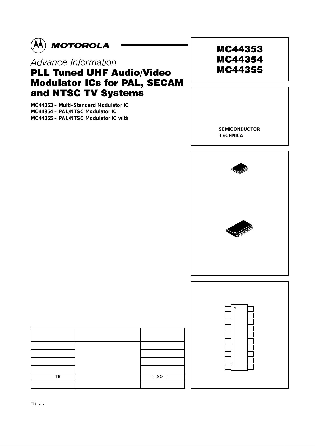
SEMICONDUCTOR
TECHNICAL DATA
MULTI–STANDARD
AND PAL/NTSC
MODULATOR ICs
DW SUFFIX
PLASTIC PACKAGE
CASE 751D
(SO–20L)
20
1
PIN CONNECTIONS
Order this document by MC44353/D
DTB SUFFIX
PLASTIC PACKAGE
CASE 948E
(TSSOP–20)
20
1
3
11
4
5
8
9
10
(Top View)
V
CCD
Osc Gnd
Osc
Snd Fil
Snd Tun
Pre–Em
Audio In
12
V
CCA
13
Video In
14
Mod Gnd
15
RF Out
16
VCC Mod
17
Mod Gnd
6Osc
7Osc Gnd
18
SCL
120
2
Amp In
Op Out
Xtal
19
SDA
1
MOTOROLA ANALOG IC DEVICE DATA
! !
!
"
MC44353 – Multi–Standard Modulator IC
MC44354 – PAL/NTSC Modulator IC
MC44355 – PAL/NTSC Modulator IC with
MC44355 – Fixed Video Modulation Index
These modulator circuits are intended for use in VCRs, satellite receivers,
set–top boxes, video games, etc. An on–chip high speed I2C compatible bus
receiver is included and is used to set the channel, tuned by a PLL over the
full range in the UHF bands. The modulator incorporates a sound subcarrier
oscillator, using a second PLL to derive 4.5, 5.5, 6.0 and 6.5 MHz carrier
frequencies, selectable by the bus.
For the sound, either frequency modulation with pre–emphasis or
amplitude modulation (MC44353 only) is possible. A control bit (MC44353
only) is used to select AM sound with positive RF modulation (system L). The
level of the sound carrier with respect to the vision carrier and the modulation
depth of both sound and vision may be adjusted by means of the bus. In
addition, an on–chip video test pattern generator may be switched in with a
1.0 kHz audio test signal.
• Channel 21 through 69 UHF Operation (471 MHz to 855 MHz)
• On–Chip Low Power Operational Amplifier for Direct Tuning Varactor
Voltage
• Single–Ended Output for Low Cost and Ease of Interface
• Low External Component Count
• High Speed I
2
C Bus Compatible
• Programmable Video Modulation Depth (8 Steps of 2.5%)
• Programmable Picture/Sound Carriers Ratio and Audio Sensitivity
(8 Steps of 1.0 dB)
• On–Chip Programmable Sound Subcarrier Oscillator (4.5 MHz to
6.5 MHz)
• On–Chip Video Test Pattern Generator with Sound Test Signal (1.0 kHz)
• V
CC
Standby Mode (Typ 500 µA)
• Transient Output Inhibit During PLL Lock–Up at Power–On
ORDERING INFORMATION
Device
Operating
Temperature Range
Package
MC44353DTB
TSSOP–20
MC44353DW
SO–20L
MC44354DTB
–
°
°
TSSOP–20
MC44354DW
T
A
= –
20° to +80°C
SO–20L
MC44355DTB TSSOP–20
MC44355DW SO–20L
This document contains information on a new product. Specifications and information herein
are subject to change without notice.
Motorola, Inc. 1998 Rev 0
Page 2
MC44353 MC44354 MC44355
2
MOTOROLA ANALOG IC DEVICE DATA
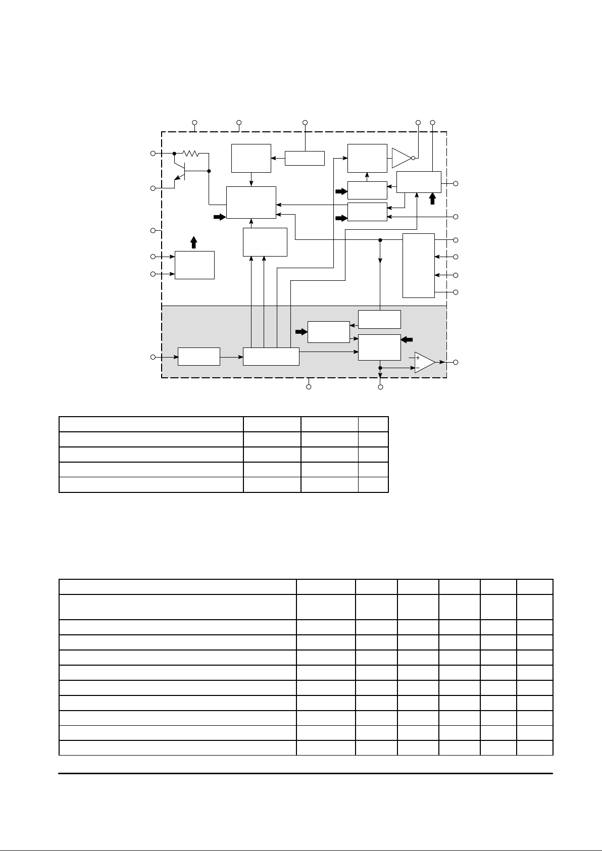
Figure 1. MC44353 Simplified Block Diagram
Modulator
Section
PLL
Section
10
11
7
6
5
4
2
13
98131412
16
15
17
18
19
20
VCC Mod Standby
RF Out
Mod Gnd
SCL
SDA
Xtal
Pre–Em
Audio
Osc Gnd
Osc
Osc
Osc Gnd
Op Out
V
CCA
Mod Gnd Video In Snd Fil Snd Tun
V
CCD
Amp In
MC44353
Peak
White Clip
Clamp
Phase/
Freq Comp
Sound Osc
+ FM Mod
Prog Divider
AM Mod
Video
Modulator
+ Sound Mix
Test Pattern
Generator
High
Speed Bus
UHF
Osc
and
Drives
÷
8
Prescaler
Phase
Comp
Prog
Divider
Ref DividerRef Osc
8
2
3
3
30
12
3
7.8 kHz
976 Hz
TE2TE1
31.25 kHz
Bias
MAXIMUM RATINGS (Note 1)
Rating Symbol Value Unit
Supply Voltage V
CC
7 V
Operational Amplifier Output Voltage 36 V
Operating Ambient Temperature T
A
–20 to 80 °C
Storage Temperature T
stg
–65 to 150 °C
NOTES: 1. Maximum ratings are those values beyond which damage to the device may occur. For
functional operation, voltages should be restricted to the Recommended Operating Conditions.
2.ESD data available upon request.
ELECTRICAL CHARACTERISTICS (Parameter Type: A–100% Tested, B–100% Correlation T ested, C–Characterized on
Samples. D–Design Parameter, VCC = 5.0 V, TA = 25C, Video input 1.0 Vpp, 10 step greyscale. Step 3 [typ. 80%] modulation depth for
PAL; Step 5 [typ 90%] modulation for SECAM L; P/S ration Step 3 [typ 14.5 dB]. RF output into 75 Ω load. Unless otherwise noted.)
(Specifications only valid for envelope demodulation.)
Characteristic
Symbol Min Typ Max Unit Type
Operating Supply Voltage Range V
CCA,VCCD
,
VCC Mod
4.5 5.0 5.5 V D
Analog Section Supply Current (VCC = 5.0 V) I
CCA
26 33 39.5 mA A
Digital Section Supply Current (VCC = 5.0 V) I
CCD
24 32 39 mA A
Modulator O/P Section Supply Current (VCC = 5.0 V) ICC Mod 6.0 9.0 11.5 mA A
Total Supply Current (VCC = 5.0 V) I
CC
56 74 90 mA A
During Standby VCC Mod 4.0 – 5.5 V D
During Standby (with Data Retension: VCC Mod = 5.0V) ICC Mod – 0.5 1.0 mA B
Operational Amplifier Output Voltage (through R
pullup
) – 30 35 V B
Operational Amplifier Output Current (with Rpullup = 560 kΩ – 56 100 µA B
Test Pattern Sync Pulse Width T
E1
4.0 4.7 5.6 µs A
Page 3
MC44353 MC44354 MC44355
3
MOTOROLA ANALOG IC DEVICE DATA
ELECTRICAL CHARACTERISTICS (continued) (Parameter Type: A–100% Tested, B–100% Correlation T ested, C–Characterized on
Samples. D–Design Parameter, VCC = 5.0 V, TA = 25C, Video input 1.0 Vpp, 10 step greyscale. Step 3 [typ. 80%] modulation depth for
PAL; Step 5 [typ 90%] modulation for SECAM L; P/S ration Step 3 [typ 14.5 dB]. RF output into 75 Ω load. Unless otherwise noted.)
(Specifications only valid for envelope demodulation.)
Characteristic TypeUnitMaxTypMinSymbol
UHF Comparator Pump Current (Note 1) 2.0 4.0 6.0 µA A
Sound Comparator Pump Current (Note 2) 2.0 3.8 5.6 µA A
Op–Amp Input Current – – 20 nA A
Oscillator Stability – negative resistance 1.0 – – kΩ D
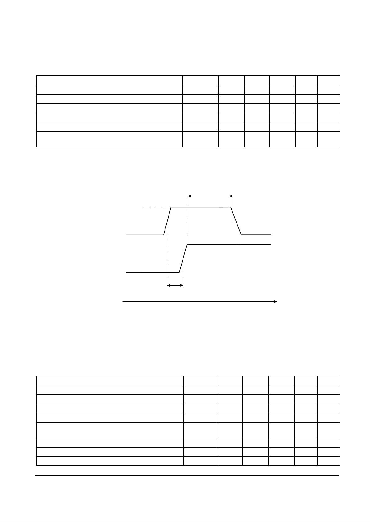
Delay V
CCA/D
to VCC Mod Application (See Figure 2) t_sup_del 0 – – ns D
V
CCA/D
& VCC Mod Duration for Standby Mode Function
(See Figure 2)
t_sup_min 30 – – ms D
NOTES: 1. Current sources driven by the UHF phase comparactor, that are connected to Pin 1.
2.Current sources driven by the phase sound comparator, that are connected to Pin 8.
V
CCA/D
V
CCmod
5.0 V
0 V
0 V
t_sup_min
t_sup_del
time
0 V
5.0 V
Figure 2. Initial Power–On and Standby Mode VCC Timing Diagram
For proper operation of internal reset functions, V
CCA
and
V
CCD
(which must be applied simultaneously) may not be
applied after V
CCmod
.
Normally, all VCC lines will come up at the same time.
However, due to the possibility of a Standby VCC to be
applied to the V
CCmod
pin, care should be ensured that
V
CCmod
is not applied before V
CCA
and V
CCD
(which must be
tied together). See the timing diagram and DATA
RETENTION function description.
Note that V
CCA/D
and V
CCmod
must be activated above 4.5
V for a least 30 msecs before the device can operate
correctly in Standby Mode.
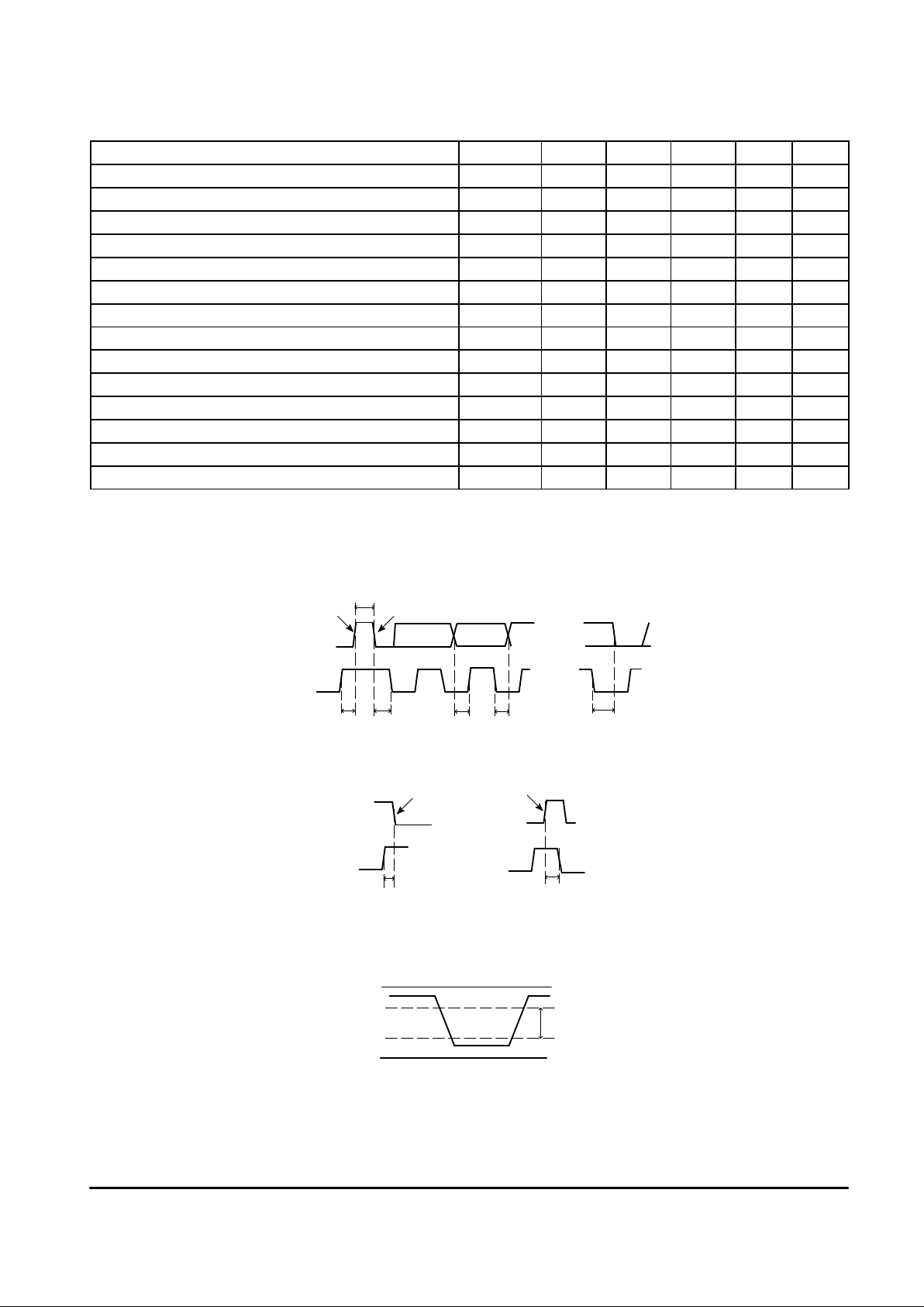
HIGH SPEED I2C COMPATIBLE BUS CHARACTERISTICS
(Over Functional Temperature Range – VCC = 5.0 V)
Characteristic
Symbol Min Typ Max Unit Type
SDA/SCL Output Current at 0 V – – 10 µA A
SDA/SCL Low Input Level V
il
– – 1.5 V B
SDA/SCL High Input Level V
ih
3.0 – – V B
SDA/SCL Input Current for Input Level from 0.4 V to 0.3 V
CC
–5.0 – 5.0 µA C
SDA/SCL Input Level 0 – VCC
+ 0.3
V D
SDA/SCL Capacitance C
i
– – 10 pF C
ACK Low Output Level (sinking 3.0 mA) – 0.3 1.0 V A
ACK Low Output Level (sinking 15 mA) – – 1.5 V C
Page 4
MC44353 MC44354 MC44355
4
MOTOROLA ANALOG IC DEVICE DATA
HIGH SPEED I2C COMPATIBLE BUS CHARACTERISTICS
(continued) (Over Functional T emperature Range – VCC = 5.0 V)
Characteristic TypeUnitMaxTypMinSymbol
Bus Clock Frequency 0 – 800 kHz C
Bus Free Time Between Stop and Start T
buf
200 – – ns C
Setup Time for Start Conditions T
su;sta
500 – – ns C
Hold Time for Start Condition T
hd;sta
500 – – ns C
Data Setup Time T
su;dat
0 – – ns C
Data Hold Time T
hd;dat
0 – – ns C
Setup Time for Stop Condition T
su;sto
500 – – ns C
Hold time for Stop Condition T
hd;sto
500 – – ns C
Acknowledge Propagation Delay T
ack;low
– – 300 ns C
SDA Fall Time at 3.0 mA sink and 130 pF Load – – 50 ns C
SDA Fall Time at 3.0 mA sink and 400 pF Load – – 80 ns C
SDA/SCL Rise Time – – 300 ns C
SCL Fall Time – – 300 ns C
Pulse Width of Spikes Suppressed by the Input Filter T
sp
– – 50 ns C
0 V
V
CC
V
IH
V
IL
Not Defined
T
buf
T
hd;dat
T
su;dat
T
su;stoThd;sta
T
ack:low
Start
Stop
T
su;sta
Chip address
T
hd;sto
Start
Stop
SDA
SCL
SDA
SCL
SDA
SCL
ACK
Figure 3. Timings Definition
Figure 4. Levels Definition
Page 5
MC44353 MC44354 MC44355
5
MOTOROLA ANALOG IC DEVICE DATA
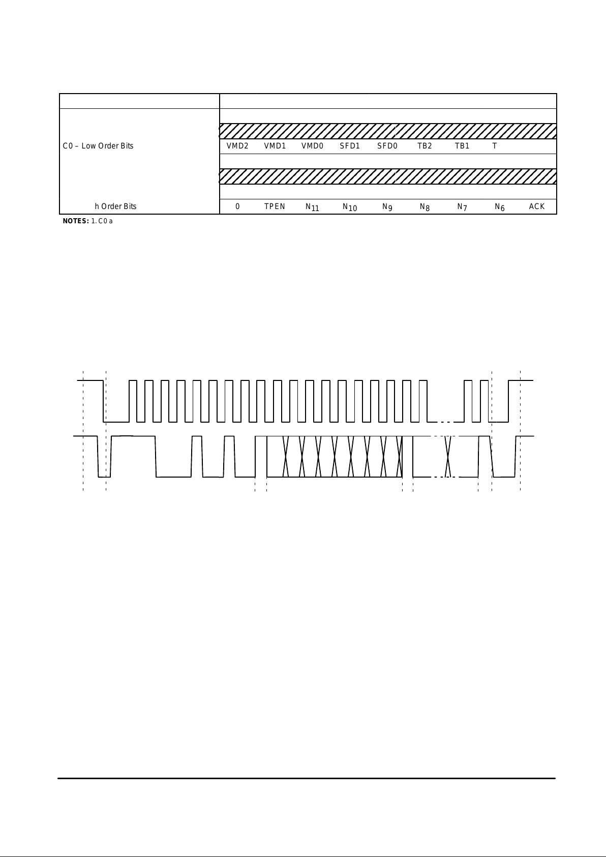
High Speed I2C Compatible Bus Format
Bit 7 Bit 0 ACK
CA – Chip Address 1 1 0 0 1 0 1 0 ACK
C0 – Low Order Bits VMD2 VMD1 VMD0 SFD1 SFD0 TB2 TB1 TB0 ACK
C1 – High Order Bits 1 AMD2 AMD1 AMD0 PSD2 PSD1 PSD0 SysL ACK
FL – Low Order Bits N
5
N
4
N
3
N
2
N
1
N
0
X
1
X
0
ACK
FM – High Order Bits 0 TPEN N
11
N
10
N
9
N
8
N
7
N
6
ACK
NOTES: 1. C0 and FL: Low Order Bits and C1 and FM: High Order Bits.
2.VDM0–2: Video Mod Depth control bits (for MC44355 VMD0–2 are Don’t Care).
3.SFD0–1: Sound subcarrier frequency control bits.
4.TB0–2 and X1, X0: T est modes bits, see table entitled TEST MODES.
5.AMD0–2: Audio Modulation Sensitivity, see table entitled AUDIO MODULATION SENSITIVITY (for MC44355 AMD0–2 are Don’t Care).
6.PSD0–2: Picture to Sound carrier ratio, see table entitled PICTURE to SOUND CARRIER RATIO (for MC44355 PSD0–1 are Don’t Care).
7.SysL: System L enable (selects AM sound and positive video modulation, MC44353 only).
8.TPEN: T est pattern enable (picture and sound).
9.N0 to N11: UHF frequency programming bits, in steps of 250 kHz.
DataFirst Data Byte (C1 or FM)
Figure 5. High Speed I2C Compatible bus data format
Chip Address ($CA)
SCL
STA
SDA
ACK
ACK ACK
12345678910111213141516171819 4445
STO
Page 6
MC44353 MC44354 MC44355
6
MOTOROLA ANALOG IC DEVICE DATA
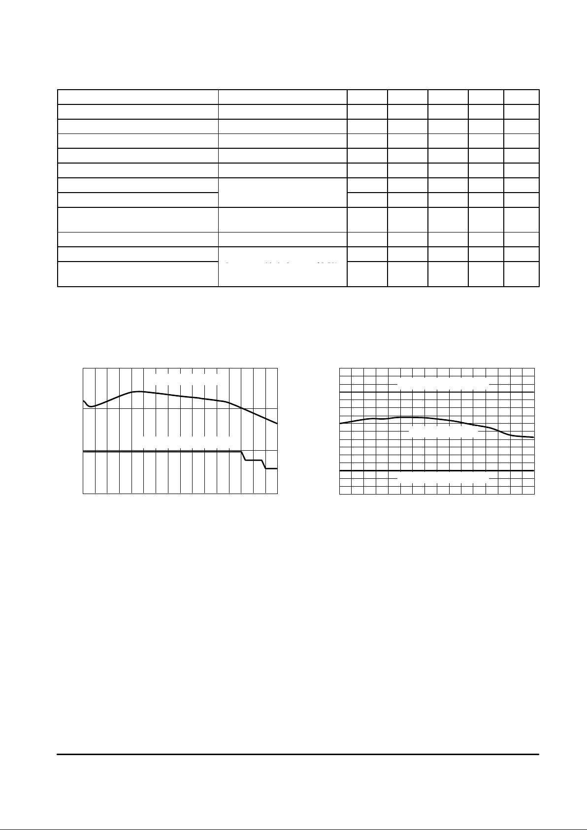
VIDEO CHARACTERISTICS
Characteristic
Test Conditions Min Typ Max Unit Type
Video Bandwidth (0/–1.0 dB; ref 0 dB @ 100 kHz) 5 - – MHz C
Video Input Level – – 1.5 V
CVBS
D
Video Input Current – 50 200 nA A
Peak White Clip (Note 1) 108 112 116 % B
Video Input Impedance Measured at 1.0 kHz (at Pin 13) – 500/4 – kΩ/pF D
Video S/N
– Figure 6 Figure 6 dB C
Differential Phase
See Note 2
Figure 7 Figure 7 Figure 7 ° C
Differentical Gain On line CCIR 310, worst from the
first 4 steps out of 5
– 1.0 5 % C
Luma/Sync ratio Input ratio 7.0:3.0 6.8/3.2 – 7.2/2.8 B
PAL V ideo Modulation Depth Step 3
76 82 88 % B
SECAM Video Modulation Depth
Step 5 (MC44353 Only)
Programmable in 8 steps of 2.5%
84.5 90.5 96.5 % B
NOTES: 1. The circuit is equipped with a ’soft clip’ function. The Video Modulation depth is measured for a 1.0 V
CVBS
input level, giving modulation depth
MDA; then the same measurement is carried out for an input level of 1.5 V
CVBS
, giving modulation depth MDB. The Peak White Clip is defined as
100*(MDB)/(MBA).
2.The frequency dependent specifications are greatly influenced by the PCB layout in the application. These specifications have all been measured
using a Motorola application layout and circuit similarly as shown in Figures 19 and 21. The reference number for ordering this evaluation board
is MC44350EVK.
–6.0
60
21
dB
Channel Number
24 27 30 33 36 39 42 45 48 51 54 57 60 63 66 69
55
50
45
Typical Performance
Maximum Specification Limit
21
Degrees
Channel Number
24 27 30 33 36 39 42 45 48 51 54 57 60 63 66 69
–8.0
Typical Performance
Maximum Specification Limit
–4.0
–2.0
0
2.0
4.0
6.0
8.0
Minimum Specification Limit
Figure 6. Video Signal to Noise Figure 7. Differential Phase
Page 7

MC44353 MC44354 MC44355
7
MOTOROLA ANALOG IC DEVICE DATA
AUDIO CHARACTERISTICS
Characteristic
Test Conditions Min Typ Max Unit Type
Audio input level AM Step 3, (SECAM)
for 85% AM modulation of sound
240 290 340 mVrms B @
fs = 6.5 MHz, (for 8 steps see Table 4 –
MC44353 Only)
subcarrier
6.5
MHz
Audio input level FM Step 3
240 305 370 mVrms B @
fs = 5.5, 6.0 or 6.5 MHz, (for 8 steps see
table 4 – MC44353/4 Only
for +/– 40 kHz deviation using
5.5
MHz
Audio input Level FM
spec
ified
pre–emphasis circuit
(FM)
, Audio frequency= 1.0 kHz
155 195 235 mVrms B @
fs = 5.5, 6.0 or 6.5 MHz (MC44355 Only)
(FM), Audio frequency= 1.0 kHz
5.5
MHz
Audio input level FM Step 3
240 305 370 mVrms D
fs = 4.5 MHz (NTSC), (for 8 steps see
table 4 – MC44353/4 Only
for ±20 kHz deviation using
specified pre–emphasis circuit
Audio input Level FM
ppp
(FM), Audio frequency= 1.0 kHz
155 195 235 mVrms D
fs = 4.5 MHz (NTSC) (MC44355 Only)
Audio input resistance at 15 kHz 30 50 75 kΩ B
Audio Frequency response
Minimum –3.0 dB; ref 1.0 kHz; using
specified pre–emphasis circuit
– – 40 Hz D
Minimum
–1.5 dB; ref 1.0 kHz; using
– – 60 Hz D
Maximum
;;g
specified pre–emphasis circuit
15 – – kHz D
Audio Distortion FM (THD only) @ 1.0 kHz; 100% mod (±50 kHz
No Video
– 0.4 2 % C
Audio Distortion AM (THD only) @ 1.0 kHz; 85% mod, No Video – 1.5 2.5 % D
Audio S/N with Sync Buzz FM See Figure 8 – Figure 8 Figure 8 dB C
Audio S/N with Sync Buzz AM Ref 1 khz; 85% mod; Video input
EBU color bar 75%; Audio BW 40
Hz to 15 kHz – Weighing filter
CCIR 468–2
45 50 – dB D
Sound/Picture ratio Step 3 (8 steps of 1.0
dB, see table P/S Ratio – MC44353/4
only)
Step 3 (typ 80%) PAL & Step 1
(typ 80%) SECAM Video Mod
depth
11 14.5 18 dB B
Sound/Picture ratio Step 5 (2 settings, see
table P/S Ratio – MC44355 only)
13 16.5 20 dB B
NOTE: 1.The frequency dependent specifications are greatly influenced by the PCB layout in the application. These specifications have all been measured
using a Motorola application layout and circuit similarly as shown in Figures 19 and 21. The reference number for ordering this evaluation board
is MC44350EVK.
60
21
dB
Channel Number
24 27 30 33 36 39 42 45 48 51 54 57 60 63 66 69
55
50
45
Typical Performance
Maximum Specification Limit
Figure 8. Audio Signal to Noise
Page 8

MC44353 MC44354 MC44355
8
MOTOROLA ANALOG IC DEVICE DATA
HIGH FREQUENCY CHARACTERISTICS
Characteristic
Test Conditions Min Typ Max Unit Type
RF Output Level See Note 1 and Figure 9. Figure 9 Figure 9 Figure 9 dbµV B
Output Inhibit Attenuation See Note 1 and Figure 10. Figure 10 Figure 10 Figure 10 dB C
UHF Oscillator Frequency Minimum Using specified circuit – – 450 MHz D
UHF Oscillator Frequency Maximum Using specified circuit 860 – – MHz D
Sound Subcarrier Harmonics (fp + n*fs) Ref Picture carrier – –62 –54 dBc Max: D
Typ: C
Second Harmonic of chroma subcarrier Using red EBU bar – –71 –60 dBc C
Chroma/Sound Intermodualtion: Using red EBU bar – –81 –72 dBc C
fp + (f
snd
– f
chr
)
FO (picture carrier) Spurious See Note 1 and Figure 11. – Figure 11 Figure 11 db µV C
FO (picture carrier) Harmonics See Note 1 and Figure 12. – Figure 12 Figure 12 dbµV C
In band spurious (fo ±5.0 MHz) No video or sound modulation – – –75 dBc C
F0 + F1 Intermodulation Product FO = 599.25 MHz
F1 = 200 MHZ (at 80 dBµV
F0 + F1 = 799.25 MHz
– – –60 dBc D
NOTE: 1.The frequency dependent specifications are greatly influenced by the PCB layout in the application. These specifications have all been measured
using a Motorola application layout and circuit similarly as shown in Figures 19 and 21. The reference number for ordering this evaluation board
is MC44350EVK.
83
70
dB V
µ
65
dB V
µ
50
86
21
dB V
Channel Number
24 27 30 33 36 39 42 45 48 51 54 57 60 63 66 69
84
82
80
Typical Performance
Maximum Specification Limit
Minimum Specification Limit
81
85
Typical Performance
Maximum Specification Limit
65
21
dB
Channel Number
24 27 30 33 36 39 42 45 48 51 54 57 60 63 66 69
55
45
35
40
60
Figure 9. RF Output Level Figure 10. RF Output Inhibit Attenuation
Frequency MHz Frequency MHz
Figure 11. FO (Picture Carrier) Spurious Figure 12. FO (Picture Carrier) Harmonics
90
50
150 250 350 450 550 650 750 850 950 1050 1150 1250
80
70
60
50
40
30
20
10
0
–10
–20
450 650 850 1050 1250 1450 1650 1850 2050 2250 2450 2650
85
80
75
60
55
50
45
40
RF Output Level
RF Output
Level
Typical Performance
Maximum Specification Limit
Maximum Specification Limit
Typical Performance
µ
2F
O
3F
O
Page 9

MC44353 MC44354 MC44355
9
MOTOROLA ANALOG IC DEVICE DATA
MODULA T OR FUNCTIONAL DESCRIPTION
General
The device has two main sections; a PLL section to
synthesize the channel frequency of the UHF output and a
modulator section which accepts audio and video inputs and
modulates the UHF carrier with them.
The channel frequency, sound and picture modulation
index and sound/picture carrier ratio are all programmable by
means of a high speed I2C compatible bus. An on–chip video
test pattern generator with an audio test signal is also
included.
The MC44353 is designed to operate as a multi–standard
modulator and can handle the systems B/G, D/K, H, I, L and
N with the same external circuit components. The basic
elements of the circuit are shown in Figure 1.
The Bus Receiver
The bus receiver operates I2C compatible bus data
format. Additional information on the data format is given on
page 5. The chip address (I2C bus) is: 1 1 0 0 1 0 1 0 (ACK)
= $CA (hex). Each ninth data bit (bits 9, 18, 27, 36 and 45) is
an ACK (acknowledge bit) during which the MCU sends a
logic “1” and the Modulator circuit answers on the data line by
pulling low. Besides the chip address the circuit needs 4 data
bytes for operation. These bytes are defined in the section on
control bits. The following sequences of data bytes are
permitted:
Example 1 CA C1 C0
Example 2 CA FM FL
Example 3 CA C1 C0 FM FL
Example 4 CA FM FL C1 C0
For the significance of the control bits the section on
control and test bit assignments on pages 11 and 12 should
be consulted.
PLL SECTION
The programmable divider
The programmable divider’s division ratio is controlled by
the state of control bits N0 to N11. The division ratio is given
by:
N = 2048*N11+ 1024*N10 + . . . . + 4*N2 + 2*N1 + N0.
Max. ratio = 4095
Min. ratio = 17.
The prescaler
The prescaler is a fixed divide by 8 and is permanently
engaged. It has a pre–amplifier for high sensitivity and good
decoupling from the RF section.
The phase comparator
The phase comparator has a current source/sink
characteristic (charge pump, see Figure 13). The pump
current is 4.0 µA. In normal operation (State 4) the phase
comparator pulls high if the UHF oscillator frequency is too
high. An internal amplifier is provided to generate tuning
voltages greater than 5.0 V while inverting the output.
The phase comparator can also be programmed to work
(in state 0) with the opposite charge pump polarity. In this
case the phase comparator pulls low if the UHF frequency is
too high. In this mode the amplifier is not required. The filter
components may be connected directly to the phase
comparator output pin. The tuning voltage range is then from
just above 0 V to VCC (5.0 V typical) and therefore not all
channels can be synthesised without adjusting the circuit
inductance.
Control bits T0, T1 and T2 are used to control the
operational state of the phase comparator. A truth table is
shown in the control bits section.
STATE 4: Normal operation with
inverted charge polarity.
10 nF
4.7 nF
240 k
Ω
560 k
Ω
Bias
Amp In
330 pF
Op Out
30 V
V
CC
On/Off
On/Off
Gnd
4.0
µ
A
4.0
µ
A
Amp In
Amp In
10 nF
4.7 nF
240 k
Ω
STATE 0: Normal operations with non–inverted
charge polarity.
Figure 13. Output Configuration of
the Phase Comparator
The reference divider
This divider divides by 128 resulting in a reference
frequency of 31.25 kHz with a 4.0 MHz crystal. The UHF
oscillator frequency may be synthesised in steps of 250 kHz.
The 250 kHz steps are due to the presence of a divide by 8
prescaler prior to the programmable divider. The reference
divider also generates the timing signals TE1 and TE2 for the
on-chip test pattern generator and the audio test signal. The
reference divider also provides the 7.8 kHz reference
frequency for the Sound PLL.
Page 10

MC44353 MC44354 MC44355
10
MOTOROLA ANALOG IC DEVICE DATA
Test Pattern Generator
A simple test pattern is generated on the IC which can be
switched in under bus control to permit a TV receiver to easily
tune in to the modulator output. The pattern consists of two
white vertical bars on a black background and a 976 Hz audio
test signal.
30
28
3/10
Figure 14. TPSG Typical Video Waveform
TE2
TE1
7/10
01020
24
40
44
50 60
64
Time in
µ
S
MODULATOR SECTION
Video Input–Clamp and Peak White Clip
The modulator requires a composite video input with
negative going sync pulses and a nominal level of 1.0 Vpp.
This signal is ac coupled to the video input where the sync tip
level is clamped.
The video signal is then passed to a peak white clip circuit
whose function is to soft clip the top of the video waveform if
the amplitude from the sync tip to peak white goes too high.
In this way over-modulation of the carrier by the video is
avoided.
Sound Subcarrier Modulator
The sound modulator system consists of an FM modulator
incorporating the sound subcarrier oscillator, and an AM
modulator. The audio input signal is ac coupled into the
amplifier which then drives the two types of modulator. In
order to provide the accuracy needed for sound subcarrier
frequencies, the sound oscillator consists of a
phase/frequency locked loop. An external LC tank circuit is
required, and the oscillator frequency is controlled by varicap
tuning diodes. The resulting oscillator frequency is divided
down by a divider whose ratio can be controlled via the bus.
A phase/frequency comparator is then used to compare this
frequency with a reference frequency (Fref 2), obtained from
the main PLL Section. The resulting error voltage is used to
control the varicap. To allow all tuning voltage to be derived
from VCC, a hyper–abrupt type of tuning diode is required to
cover the necessary capacitance range. If only a single
sound subcarrier frequency is being used, for example for
PAL only or NTSC, then a less abrupt varicap diode may be
used. The sound phase frequency comparator also requires
an external loop filter.
The oscillator provides subcarrier frequencies of 4.5, 5.5,
6.0 and 6.5 MHz, selectable via the bus. For all applications
except system L, the subcarrier is frequency modulated with
the audio signal. For system L, amplitude modulation is
employed. The level of audio at the input needed to give the
maximum permissible modulation depth (50 kHz FM
deviation, 85% AM depth), may be adjusted under bus
control.
UHF Oscillator
The UHF oscillator is designed to operate over a range of
450 to 860 MHz. The oscillator drives an external LC tank
circuit differentially, and is tuned by a varicap diode. The
varicap tuning voltage, as described in an earlier section, is
provided from an on chip operational amplifier and external
filter arrangement which is controlled by the PLL Section of
the chip. The UHF frequency thus generated is used by the
modulator as the TV channel carrier frequency.
Video Modulator and Sound Mixer
This section of the circuit accepts as inputs:
1. composite video;
2. the selected sound subcarrier I2C frequency;
3. the UHF carrier frequency at the selected channel;
4. the test pattern generator waveform.
Selection is made via the control bus between the
composite video input and the on chip test pattern generator.
The video and sound inter-carrier are used to amplitude
modulate the UHF carrier. Negative modulation is used,
except in the case of System L where positive modulation is
used.In this part of the circuit, the video modulation depth and
the sound to picture carrier ratio may be programmed under
bus control. In system L mode the video modulation depth
has the same range, but may extend to higher percentage
values.
RF O/P Buffer
The TV signal generated in the video modulator and mixer
section is fed to an emitter follower output stage, capable of
driving a terminated line. This output is provided with a
separate VCC pin in order to avoid large circulating currents
on the IC. It can provide at the output typically 84 dBµV of
signal across a 75 Ω load.
Transient Output Inhibit
To minimize the risk of interference to other channels
while the UHF PLL is acquiring lock on the desired frequency
at Power-on, the UHF output stages are turned off for each
power-on from zero and from standby mode. There is a
timeout of 263 ms until the output is enabled. This allows the
PLL to settle on its programmed frequency. Care must be
taken therefore in determining the loop filter components so
that the loop transient does not exceed this delay.
Data Retention
The circuit contains 4 bytes of memory holding the last
frequency and control bits information. The circuit can retain
this information at power down if a suitable VCC is supplied.
The Standby VCC of nominal 5.0 V must be applied to pin
VCC Mod. The 5.0 V current in data retention is approximately
500 µA. Note that the voltage source on this pin must be able
to supply a much higher current in normal operation (typically
12 mA).
The circuit will enter into Data Retention Mode when the
V
CCA
pin voltage drops below approximately 3.0 V.
Page 11

MC44353 MC44354 MC44355
11
MOTOROLA ANALOG IC DEVICE DATA
Test Modes
Various test modes can be enabled, by means of bits
TB0–2 and X0–1. These operate by assigning some internal
signals on the UHF phase comparator output current sources
as outlined in the following 2 tables.
Table 1. Test Mode 1
Test Bits TB0 to TB2 are located in C0, bits 0 to 2:
TB2 TB1 TB0 State Function
0 0 0 0 See Table Test Mode 2
Normal Operation, But Test
001
1
Pattern Geneartor Disabled
Upper Source On, Lower
010
2
Source Off
Lower Source On, Upper
011
3
Source Off
Normal Operation with
100
4
Inverted Charge Polarity
High Impedance
101
5
Test Ref divider on Upper
110
6
Source (F
ref
), Lower Source Off
Test Progr. divider on Lower
111
7
Source (F
out/2
), Upper Source Off
Table 2. Test Mode 2
Bits X0 and X1 are located in FL, bits 0 and 1:
X1 X0
State
Function
Normal Operation with Non–Inverted
000a
Charge Pump Polarity
Normal Inverted Operation (same as
0 1 0b mode 4), but Transient Output Inhibit
Disabled.
Normal Inverted Operation (same as
1 0 0c mode 4), but Transient Output Inhibit
Circuitry Forced (output disabled).
Normal Inverted Operation (same as
1 1 0d mode 4), but Transient Output Inhibit
counter Sped up (64 times).
In normal operation, the phase comparator pulls high if the
UHF frequency is too high, and pulls low when the UHF
frequency is too low. This mode is used when the tuning
voltage is generated by the internal inverting operational
amplifier, so in this case mode 4 (100) must be used.
Switching in mode 0d will reset the transient delay counter,
which will time out at an accelerated rate of 64 times the
normal rate.
Sound Section Test Modes
The Sound PLL is tested in a similar fashion, and
responds to States 6 and 7 by placing the output of the sound
PLL programmable divider on the upper current source.
Table 3. Sound Subcarrier Frequency
SFD1 SFD0 Sound Subcarrier Freq (MHz)
0 0 4.5
0 1 5.5
1 0 6.0
1 1 6.5
NOTE: 1. Bits SFD1–0 are located in C0 bits 4 and 3.
Figure 15. CCIR Test Line 330
*1.0
0.86
0.72
0.58
0.44
**0.3
Step 0
1
234
5
NOTE: Not to scale
*100 IRE
** 1 IRE
VOLTS
40
–16
Approximately Characteristic of Standard
Independent Filter in conformity with CCIR Rec. 567
0
–4
–8
–12
012345
a
f
Decibels
MHz
Figure 16. Noise Measurement/Weighting Filter
Page 12

MC44353 MC44354 MC44355
12
MOTOROLA ANALOG IC DEVICE DATA
Table 4. Audio Modulation Sensitivity (Control Bits)
AMD2 AMD1 AMD0
Audio Input for FM
PAL/NTSC
(MC44353/4)
Audio Input for AM
SECAM
(MC44353 Only)
Audio Input for FM
PAL/NTSC
(MC44355 Only)
0 0 0 420 mVrms 405 mVrms Not Programmable
0 0 1 375 mVrms 365 mVrms Not Programmable
0 1 0 335 mVrms 325 mVrms Not Programmable
0 1 1 300 mVrms 290 mVrms Not Programmable
1 0 0 270 mVrms 260 mVrms Not Programmable
1 0 1 240 mVrms 230 mVrms Not Programmable
1 1 0 215 mVrms 205 mVrms Not Programmable
1 1 1 190 mVrms 185 mVrms 190 mVrms
NOTE: 1. Audio sensitivity bits AMD2–0 are located in C1 bits 6 to 4.
Table 5. Picture to Sound Carrier Ratio (Control Bits)
PSD2 PSD1 PSD0
P/S Carrier Ratio
(MC44353/4)
P/S Carrier Ratio
(MC44355 Only)
0 0 0 11.5 dB Not Programmable
0 0 1 12.5 dB 12.5 dB
0 1 0 13.5 dB Not Programmable
0 1 1 14.5 dB Not Programmable
1 0 0 15.5 dB Not Programmable
1 0 1 16.5 dB 16.5 dB
1 1 0 17.5 dB Not Programmable
1 1 1 18.5 dB Not Programmable
NOTE: 1. Picture to sound carriers ratio bits PSD2–0 are located in C1 bits 3 to 1.
Table 6. Video Modulation Depth (Control Bits)
VMD2 VMD1 VMD0
Video Mod Depth
PAL
(MC44353/4)
Video Mod Depth
SECAM
(MC44353 Only)
Video Mod Depth
PAL
(MC44355 Only)
0 0 0 74.5% 78% Not Programmable
0 0 1 77% 80.5% Not Programmable
0 1 0 79.5% 83% Not Programmable
0 1 1 82% 85.5% 82%
1 0 0 84.5% 88% Not Programmable
1 0 1 87% 90.5% Not Programmable
1 1 0 89.5% 93% Not Programmable
1 1 1 92% 95.5% Not Programmable
NOTES: 1. Video modulation depth bits VMD2–0 are located in C0 bits 7 to 5.
2.SECAM values are approximately 5% higher than PAL values.
Page 13

MC44353 MC44354 MC44355
13
MOTOROLA ANALOG IC DEVICE DATA
16 Amp In
Negative input of operation
amplifier and phase detector
charge pump output
20 Xtal
Crystal oscillator
(4.0 MHz)
18 SCL
Clock input (I2C bus)
19 SDA
Data input/output (I2C bus)
14 Mod Gnd
13 Video In
Input for baseband video. Signal
modulates the RF carrier.
11 Audio In
Input for sound. Signal
modulates the sound carrier.
Snd Fil 8
Phase/Freq. detector
charge pump output
Figure 17. Pin Circuit Schematic
Op Out 1
Operational amplifier
output which provides
the tuning voltage
V
CCD
3
Digital circuit supply
Osc Gnd 7
Oscillator Ground
500
132 k
20 V
V
CC
96 k
96 k
1/2 V
CC
500
132 k
20 V
5.0 V
100
2.0 k 10 k
20 V
20 V
20 V
50
1.5 k
ACK
V
CC
96 k
96 k
1/2 V
CC
Osc Gnd 4
Oscillator Ground
Pre–Em 10
Frequency selective filter to
shape sound modulation depth.
Snd Tun 9
Sound carrier oscillator
L/C tuned circuit
5
6
Bal Osc
Balanced cross coupled oscillator
terminals. L/C resonance circuit
12 V
CCA
Audio supply voltage
15 RF Out
RF output
16 VCC Mod
17 Mod Gnd
V
CCA
72
490
V
CCA
V
CCA
24.5 k 24.5 k
50 k
1.0 p
5.0 V
5.0 V
5.0 V
5.0 V
5.0 V
5.0 V
Audio
Page 14

MC44353 MC44354 MC44355
14
MOTOROLA ANALOG IC DEVICE DATA
Figure 18. Typical Application
R10
240 k
Ω
20
19
18
17
16
15
14
13
12
11
1
2
3
4
5
6
7
8
9
10
Amp In Xtal
Op Out SDA
V
CCD
SCL
Gnd Mod Gnd
Osc1 VCC Mod
Osc2 RF Out
Gnd Mod Gnd
Snd Filt Video
Snd Tun V
CCA
Pre–Em Audio
MC44353
C22
0.1
C21
330 pF
R11
560 k
C19
0.0047
R6
33 k
Ω
C13 0.022
R5
220 k
Ω
C12
0.0022
R4
100 k
HVUR17HVUR17
L2
≈
27 µH
R8
47 k
Ω
C10
0.1
C16
0.001 (Note 2)
C17
0.001 (Note 2)
R9
47 k
Ω
D3
HVU202A
C18
0.1
R7
220 k
Ω
C9
220 pF
C8
100 pF
L1
6.8 nH
(Note 3)
30 V
V
CCT
Cx
(Note 1)
4.0 MHz
SDA
SCL
High
Speed
Bus
C1, 2
0.2
75
Ω ±
1%
C3
0.01
C5
0.001
C6
0.1
5.0 V
TV Out
Video In
Audio In
NOTES: 1. Cx depends on Crystal Load Capacitance, Crystal resistance < 200 Ω.
2.Tubular 0603 1.0 nF capacitors.
3.L1 is a 2 turn air coil.
4.L2 and R3 are non–surface mount components. Note L2 quality factor should be high enough to keep the
sound carrier at the typical level Q min @ 5.5 MHz = 43, Q min @ 6.0 MHz = 40, and Q min @ 6.5 MHz = 37.
5.C11 and L2 are selected to control the sound carrier center frequency and its tuning range.
6.D1 and D2 are hyper–abrupt varactor. Minimum capacitance ratio between 1.0 and 4.5 V is C1/C4.5 = 5.6
to cover the full frequncy range. (C @ 1.0 V = 50 pF min)
C4
0.1
R1
1.0 k
C20
0.01
C14, 15
0.22
C11
C7
10
µ
f
R2
R3
4.7
Ω
(Note 4)
(Note 5)
(Note 4)
D1 D2
Modifications to the application layout (Figures 19 through
21) will have an effect on the overall application
performances. The most sensitive areas are around the UHF
Oscillator and RF Output (Pins 4 to 7 and Pins 14 to 17) so
care must be taken to reproduce a similar PCB layout in the
final application.
Page 15

MC44353 MC44354 MC44355
15
MOTOROLA ANALOG IC DEVICE DATA
Figure 19. PCB Layout for SO–20L (Top Layer)
V
CCT
Gnd
V
CC
V
CC
Gnd
SCL
SDA
Gnd
Scale 2:1
D1
D2
C10
C11
R4
R5
C12 C14 C15
C8
R8
R7
C9
C4
C16
D3
C17
L1
C20
R10
C19
R11
C21
C18
C22
C1
C3
R2
C5
C6
Cx
P1
R1
R9
C7
C2
U1
15 Pin D
Connector
C13R6
Page 16

MC44353 MC44354 MC44355
16
MOTOROLA ANALOG IC DEVICE DATA
Figure 20. PCB Layout for TSSOP–20 (Top Layer)
V
CCT
Gnd
V
CC
V
CC
Gnd
SCL
SDA
Gnd
Scale 2:1
15 Pin D
Connector
D1
D2
C10
C11
R4
R5
C12 C14 C15
C8
R8
R7
C9
C4
C16
D3
C17
L1
C20
R10
C19
R11
C21
C18
C22
C1
C3
R2
C5
C6
Cx
P1
R1
R9
C7
C2
U1
C13R6
Page 17

MC44353 MC44354 MC44355
17
MOTOROLA ANALOG IC DEVICE DATA
Figure 21. PCB Layout for SO–20L and TSSOP–20 used for Characterization (Bottom Layer)
Scale 2:1
Page 18

MC44353 MC44354 MC44355
18
MOTOROLA ANALOG IC DEVICE DATA
DTB SUFFIX
PLASTIC PACKAGE
CASE 948E–02
(TSSOP–20)
ISSUE A
OUTLINE DIMENSION
DIMAMIN MAX MIN MAX
INCHES
6.60 0.260
MILLIMETERS
B 4.30 4.50 0.169 0.177
C 1.20 0.047
D 0.05 0.15 0.002 0.006
F 0.50 0.75 0.020 0.030
G 0.65 BSC 0.026 BSC
H 0.27 0.37 0.011 0.015
J 0.09 0.20 0.004 0.008
J1 0.09 0.16 0.004 0.006
K 0.19 0.30 0.007 0.012
K1 0.19 0.25 0.007 0.010
L 6.40 BSC 0.252 BSC
M 0 8 0 8
____
NOTES:
1 DIMENSIONING AND TOLERANCING PER ANSI
Y14.5M, 1982.
2 CONTROLLING DIMENSION: MILLIMETER.
3 DIMENSION A DOES NOT INCLUDE MOLD FLASH,
PROTRUSIONS OR GATE BURRS. MOLD FLASH
OR GATE BURRS SHALL NOT EXCEED 0.15
(0.006) PER SIDE.
4 DIMENSION B DOES NOT INCLUDE INTERLEAD
FLASH OR PROTRUSION. INTERLEAD FLASH OR
PROTRUSION SHALL NOT EXCEED 0.25 (0.010)
PER SIDE.
5 DIMENSION K DOES NOT INCLUDE DAMBAR
PROTRUSION. ALLOWABLE DAMBAR
PROTRUSION SHALL BE 0.08 (0.003) TOTAL IN
EXCESS OF THE K DIMENSION AT MAXIMUM
MATERIAL CONDITION.
6 TERMINAL NUMBERS ARE SHOWN FOR
REFERENCE ONLY.
7 DIMENSION A AND B ARE TO BE DETERMINED
AT DATUM PLANE –W–.
110
1120
PIN 1
IDENT
A
B
–T–
0.100 (0.004)
C
D
G
H
SECTION N–N
K
K1
JJ1
N
N
M
F
–W–
SEATING
PLANE
–V–
–U–
S
U
M
0.10 (0.004) V
S
T
20X REFK
L
L/2
2X
S
U0.15 (0.006) T
DETAIL E
0.25 (0.010)
DETAIL E
6.40 0.252
––– –––
S
U0.15 (0.006) T
DW SUFFIX
PLASTIC PACKAGE
CASE 751D–04
(SO–20WB)
ISSUE E
NOTES:
1. DIMENSIONING AND TOLERANCING PER
ANSI Y14.5M, 1982.
2. CONTROLLING DIMENSION: MILLIMETER.
3. DIMENSIONS A AND B DO NOT INCLUDE
MOLD PROTRUSION.
4. MAXIMUM MOLD PROTRUSION 0.150
(0.006) PER SIDE.
5. DIMENSION D DOES NOT INCLUDE
DAMBAR PROTRUSION. ALLOWABLE
DAMBAR PROTRUSION SHALL BE 0.13
(0.005) TOTAL IN EXCESS OF D DIMENSION
AT MAXIMUM MATERIAL CONDITION.
–A–
–B–
20
1
11
10
S
A
M
0.010 (0.25) B
S
T
D20X
M
B
M
0.010 (0.25)
P10X
J
F
G
18X
K
C
–T–
SEATING
PLANE
M
R
X 45
_
DIM MIN MAX MIN MAX
INCHESMILLIMETERS
A 12.65 12.95 0.499 0.510
B 7.40 7.60 0.292 0.299
C 2.35 2.65 0.093 0.104
D 0.35 0.49 0.014 0.019
F 0.50 0.90 0.020 0.035
G 1.27 BSC 0.050 BSC
J 0.25 0.32 0.010 0.012
K 0.10 0.25 0.004 0.009
M 0 7 0 7
P 10.05 10.55 0.395 0.415
R 0.25 0.75 0.010 0.029
__
__
Page 19

MC44353 MC44354 MC44355
19
MOTOROLA ANALOG IC DEVICE DATA
Motorola reserves the right to make changes without further notice to any products herein. Motorola makes no warranty , representation or guarantee regarding
the suitability of its products for any particular purpose, nor does Motorola assume any liability arising out of the application or use of any product or circuit, and
specifically disclaims any and all liability, including without limitation consequential or incidental damages. “T ypical” parameters which may be provided in Motorola
data sheets and/or specifications can and do vary in different applications and actual performance may vary over time. All operating parameters, including “Typicals”
must be validated for each customer application by customer’s technical experts. Motorola does not convey any license under its patent rights nor the rights of
others. Motorola products are not designed, intended, or authorized for use as components in systems intended for surgical implant into the body, or other
applications intended to support or sustain life, or for any other application in which the failure of the Motorola product could create a situation where personal injury
or death may occur. Should Buyer purchase or use Motorola products for any such unintended or unauthorized application, Buyer shall indemnify and hold Motorola
and its officers, employees, subsidiaries, affiliates, and distributors harmless against all claims, costs, damages, and expenses, and reasonable attorney fees
arising out of, directly or indirectly, any claim of personal injury or death associated with such unintended or unauthorized use, even if such claim alleges that
Motorola was negligent regarding the design or manufacture of the part. Motorola and are registered trademarks of Motorola, Inc. Motorola, Inc. is an Equal
Opportunity/Affirmative Action Employer.
Page 20

MC44353 MC44354 MC44355
20
MOTOROLA ANALOG IC DEVICE DATA
Mfax is a trademark of Motorola, Inc.
How to reach us:
USA/EUROPE /Locations Not Listed: Motorola Literature Distribution; JAPAN: Nippon Motorola Ltd.: SPD, Strategic Planning Office, 141,
P.O. Box 5405, Denver, Colorado 80217. 1–303–675–2140 or 1–800–441–2447 4–32–1 Nishi–Gotanda, Shagawa–ku, Tokyo, Japan. 03–5487–8488
Customer Focus Center: 1–800–521–6274
Mfax: RMFAX0@email.sps.mot.com – TOUCHTONE 1–602–244–6609 ASIA/PACIFIC: Motorola Semiconductors H.K. Ltd.; 8B Tai Ping Industrial Park,
Moto rola Fax Back System – US & Canada ONLY 1–800–774–1848 51 Ting Kok Road, Tai Po, N.T., Hong Kong. 852–26629298
– http://sps.motorola.com/mfax/
HOME PAGE: http://motorola.com/sps/
MC44353/D
◊
 Loading...