

Page 1
Device
Tested Operating
Temperature Range
Package
SEMICONDUCTOR
TECHNICAL DATA
ADVANCED
MULTI–STANDARD
VIDEO/SOUND IF
ORDERING INFORMATION
MC44302ADW
MC44302AP
TA = 0° to +70°C
SO–28L
Plastic DIP
P SUFFIX
PLASTIC PACKAGE
CASE 710
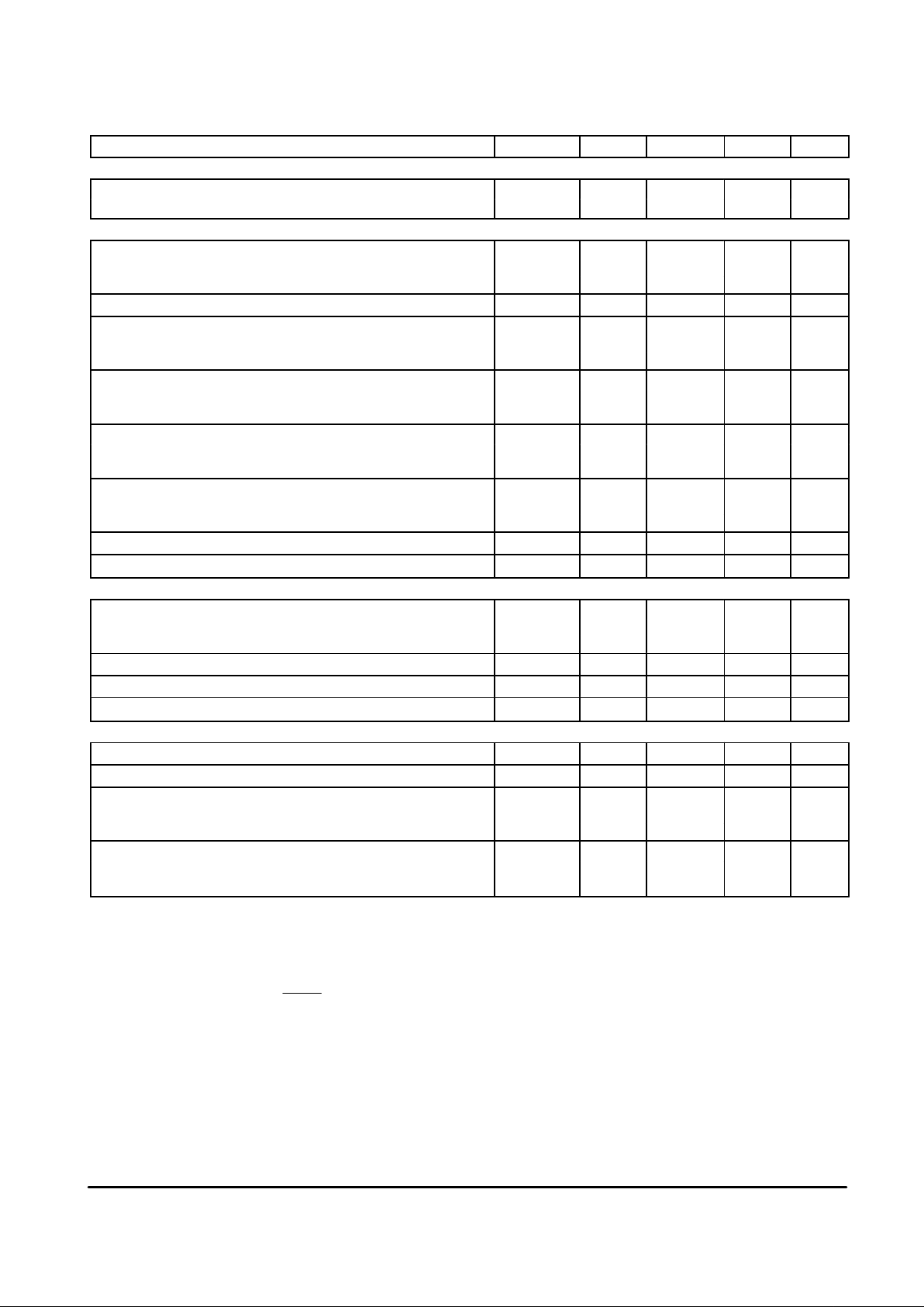
28
1
(Top View)
PIN CONNECTIONS
Order this document by MC44302A/D
28
1
DW SUFFIX
PLASTIC PACKAGE
CASE 751F
(SO–28L)
1
2
3
4
5
6
7
8
9
10
11
12
13
14
28
27
26
25
24
23
22
21
20
19
18
17
16
15
Intercarrier
Sound Output
DC Volume Control
Sound Input (FM)
Audio Input/
Audio–Video Switch
Sound
De–Emphasis (FM)
Negative Video Out
Positive Video Out
Sound AFT Filter/
Peak White Filter
Video IF Input
Video IF Input
Video Mode Switch
AFT Output
AFT Mode Switch
RF AGC Output
Video IF AGC Filter
Audio Output
(Variable)
Sound Quadrature
Coil (FM)
V
CC
Audio Output
(Constant)
Sound Input (AM)
Gnd
VCO Coil
VCO Coil
PLL Filter
(Main VCO Loop)
Lock Detector/Filter
(Acquisition Circuit)
Flyback/Video Input
Horizontal PLL Filter
RF AGC Delay
1
MOTOROLA ANALOG IC DEVICE DATA
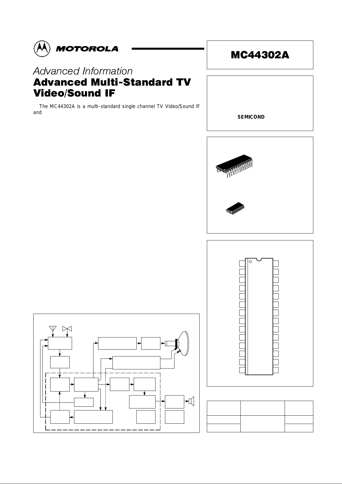
The MC44302A is a multi–standard single channel TV Video/Sound IF
and PLL detector system specifically designed for use with all standard
modulation techniques including NTSC, PAL, and SECAM. This device
enables the designer to produce a high quality IF system with a minimum
number of external components.
The MC44302A contains a high gain video IF with an AGC range of 80 dB,
enhanced phase–locked loop carrier regenerator for low static phase error,
doubly balanced full wave synchronous video demodulator featuring wide
bandwidth positive and negative video outputs with extremely low differential
gain and phase distortion, video AFT amplifier, multistage sound IF limiter
with FM quadrature detector and AFT for self tuning, AM sound detector,
constant and variable audio outputs, dc volume control for reduced hum and
noise pickup, unique signal acquisition circuit that prevents false PLL lockup
and AFT push out, horizontal gating system with sync separator and
phase–locked loop circuitry for self–contained RF/IF AGC operation, RF
AGC delay circuitry, and programmable control logic that allows operation in
NTSC, and PAL SECAM systems. This device is available in wide body 28 pin
dual–in–line and surface mount plastic packages.
• Multi–Standard Detector System for NTSC, PAL, and SECAM
• High Gain Video IF Amplifier with 80 dB AGC Range
• Enhanced PLL Carrier Regenerator for Low Static Phase Error
• Synchronous Video Demodulator with Positive and Negative Video
Outputs
• Sound IF with Self Tuning FM Quadrature Detector
• AM Sound Detector
• DC Volume Control
• Unique Signal Acquisition Circuit Prevents False PLL Lockup
• Horizontal Gating System for Self Contained RF/IF AGC Operation
• RF AGC Delay Circuitry
This document contains information on a new product. Specifications and information herein
are subject to change without notice.
Motorola, Inc. 1997 Rev 0
Simplified Television Block Diagram
DC Volume
Control
MC44302A
Vertical & Horizontal
Scan Circuitry
Power
Supply
VHF/UHF
Tuner
Video
IF
Audio
Amp
Video
Detector
Sound
IF
Sound
Detector
Video
Drivers
Luma & Chroma
Processor
SAW
Filter
Horizontal
Gating System
RF/IF
AGC
Mode
Switch
AFT
Page 2
MC44302A
2
MOTOROLA ANALOG IC DEVICE DATA
MAXIMUM RATINGS
Rating Symbol Value Unit
Power Supply Voltage
V
CC
7.0
V
Input Voltage Range
V
IR
–0.3 to V
CC
V
Video IF (Pins 8, 9)
FM Sound IF (Pin 2)
AM Sound IF (Pin 23)
AFT Switch (Pin 12)
Audio Input/Audio Switch/Video Invert (Pin 3)
Mode Switch (Pin 10)
RF AGC Delay (Pin 15)
Volume Control (Pin 1)
Sound Quadrature Coil Voltage (Pin 26)
V
QC
V
CC
V
VCO Coil Voltage (Pins 20, 21)
V
VCO
V
CC
V
Flyback/Video Input Current (Pin 17)
I
in
±1.0
mA
Output Current
I
O
mA
Positive and Negative Video (Pins 5, 6) 15
Intercarrier Sound (Pin 28) 15
Constant and Variable Audio (Pins 24, 27) 15
RF AGC, Internally Limited (Pin 13) 2.0
AFT Source or Sink (Pin 11) 4.0
Power Dissipation and Thermal Characteristics
DW Suffix, Plastic Package Case 751F
Maximum Power Dissipation @ T
A
= 70°C P
D
800 mW
Thermal Resistance, Junction–to–Air R
θJA
100 °C/W
P Suffix, Plastic Package Case 710
Maximum Power Dissipation @ T
A
= 70°C P
D
1000 mW
Thermal Resistance, Junction–to–Air R
θJA
80 °C/W
Operating Junction Temperature
T
J
+150
°C
Operating Ambient Temperature
T
A
0 to +70
°C
Storage Temperature
T
stg
–65 to +150
°C
NOTE: ESD data available upon request.
ELECTRICAL CHARACTERISTICS (V
CC
= 5.0 V , TA = 25°C.)
Characteristic
Symbol Min Typ Max Unit
VIDEO IF AMPLIFIER
Differential Input Impedance Components
Parallel Resistance R
in(VIF)
– 3.4 – kΩ
Parallel Capacitance C
in(VIF)
– 4.0 – pF
Differential Input V oltage for Full Video Output Swing DV
in(VIF)
– 40 – µVrms
Automatic Gain Control Range AGC
VIF
– 80 – dB
Noise Figure (Vin = 1.0 mV, RS = 300 Ω) NF – 7.0 – dB
Bandwidth, –3.0 dB (RS = 300 Ω) BW
VIF
– 120 – MHz
Sound Intercarrier Output, 4.5 MHz (Vin = 1.0 mV , Note 2) V
O(Snd IC)
– 0.1 – Vrms
VIDEO DETECTOR
Output Voltage Swing (Pin 5 or 6, RL = 2.0 k, Note 1) V
O(VD)
– 2.2 – Vpp
Output Impedance (Pin 5 or 6, 1.0 MHz, 1.0 mA) |ZO| – 100 – Ω
Bandwidth, –3.0 dB, (RL = 2.0 k) BW
VD
MHz
Negative Output (Pin 5) – 8.0 –
Positive Output (Pin 6) – 7.0 –
Output Distortion, Uncorrected (RL = 2.0 k, Note 1)
Differential Gain DG %
Negative Video Output – 2.0 5.0
Positive Video Output – 2.0 5.0
Differential Phase DP Deg
Negative Video Output – 1.0 5.0
Positive Video Output – 1.0 5.0
Page 3
MC44302A
3
MOTOROLA ANALOG IC DEVICE DATA
ELECTRICAL CHARACTERISTICS (continued) (V
CC
= 5.0 V , TA = 25°C.)
Characteristic UnitMaxTypMinSymbol
VIDEO DETECTOR (CONTINUED)
Residual 920 kHz Beat Output, dB Below 100% Modulated Video B
O
– –60 – dB
(Pin 5 or 6, Note 2)
FM SOUND IF AND DETECTOR
Input Impedance Components
Parallel Resistance R
in(FM)
– 2.2 – kΩ
Parallel Capacitance C
in(FM)
– 4.0 – pF
Input Limiting Threshold (f = 4.5 MHz) V
in(Snd)
– 80 – µV
AM Rejection (Vin = 10 mV, Notes 4, 5, 6) AMR dB
f = 4.5 MHz – 50 –
f = 5.5 MHz – 50 –
Recovered Audio Output (Pin 24, Vin = 10 mV , Note 4) V
O(Snd)
Vpp
f = 4.5 MHz – 2.0 –
f = 5.5 MHz – 2.0 –
Output Distortion (Pin 24, Vin = 10 mV , Note 4) THD %
f = 4.5 MHz – 1.0 –
f = 5.5 MHz – 1.0 –
Sound AFT (Note 7) ∆f
AFT(Snd)
MHz
Pull–in Range – ±0.6 –
Hold–in Range – ±0.6 –
Sound De–Emphasis Internal Resistance (Pin 4) R
DE
– 18 – kΩ
AM Detector Crosstalk Ctlk
AM
– –6.0 – dB
AM DETECTOR
Input Impedance Components
Parallel Resistance R
in(AM)
– 5.6 – kΩ
Parallel Capacitance C
in(AM)
– 4.0 – pF
Recovered Audio Output (Pin 24, Vin = 100 mV , Note 5) V
O(Snd)
– 2.0 – Vpp
Output Distortion (Pin 24, Vin = 10 mV , Note 5) THD – 1.0 – %
FM Sound IF and Detector Crosstalk Ctlk
FM
– –60 – dB
DC VOLUME CONTROL
Volume Control Range (Pin 1, Pin 3 = Vin) ∆V
O(Snd)
– +12 to –70 – dB
Output Signal at Minimum Volume Setting (Pin 1 = Gnd, Pin 3 = Vin ) V
O(Snd)
– 1.0 – mV
Video Detector Sync to Audio Channel Crosstalk Ctlk
VD
dB
Fixed Output – –60 –
Variable Output – –60 –
Audio Channel Crosstalk Ctlk
Snd
dB
Fixed Output to Variable Output – –60 –
Variable Output to Fixed Output – –60 –
NOTES: 1. V
in
= 1.0 mVrms signal at 45.75 MHz with 75% modulated staircase at 3.58 MHz.
2.Vin = 100 µVrms signal at 41.25 MHz added to signal in Note 1.
3.Differential carrier level at video IF inputs to cause the negative detector output to go positive by 0.1 V from ground.
4.FM Modulation = ±25 kHz deviation at 1.0 kHz for 4.5 MHz intercarrier.
±50 kHz deviation at 1.0 kHz for 5.5 MHz intercarrier.
5.AM Modulation = 30% depth at 1.0 kHz for 4.5 MHz and 5.5 MHz intercarrier.
6.AM Rejection (dB) = 20 log
7.Tested with 15 µH sound quadrature coil in parallel with 68 pF and 10 kΩ.
8.The AFT output can be disabled by leaving Pin 12 disconnected or by biasing it to the voltage level shown above. When disabled, the output will be
internally clamped to one half of VCC.
V
O(FM)
V
O(AM)
Page 4
MC44302A
4
MOTOROLA ANALOG IC DEVICE DATA
ELECTRICAL CHARACTERISTICS
(continued) (VCC = 5.0 V , TA = 25°C.)
Characteristic UnitMaxTypMinSymbol
PHASE–LOCKED LOOP
Acquisition Circuit Filter Voltage (Pin 18) V
PLL(Acq)
V
Unlocked with No–Signal – 2.7 –
Unlocked to Locked Sweep Range upon Signal Acquisition – 1.2 to 4.3 –
Locked, Final Static Condition – 4.3 –
VCO Filter Voltage (Pin 19) V
PLL(VCO)
V
Unlocked – 3.2 –
Locked, Final Static Condition – 3.2 –
Video IF Lock–Up Time t
IF(lock)
– 5.0 – ms
HORIZONTAL GATING SYSTEM
Sync Separator Input Threshold Voltage (Pin 17) V
th(Sync)
– 3.4 – V
PLL Filter Voltage, Locked or Unlocked with No–Signal (Pin 16) V
PLL(Horiz)
– 2.9 ± 1.1 – V
RF AGC
RF AGC Delay Voltage Range (Pin 15) V
AGC(DLY)
– 1.7 to 2.4 – V
RF AGC Output Current (Pin 13) I
O(sink)
1.0 2.0 – mA
LOGIC CONTROL
Mode Select Voltage Range (Pin 10) V
th(Mode)
V
PAL 1 4.7 to 5.0 4.6 to 5.0 –
PAL 2 3.5 to 4.1 3.4 to 4.2 –
SECAM 2.3 to 2.9 2.2 to 3.0 –
NTSC 0 to 0.3 0 to 0.4 –
AFT Switch Threshold (Pin 12) V
th(AFT)
AFT Output, Pin 11, Sourcing when IF Frequency is Low – 5.0 –
AFT Output, Pin 11, Sinking when IF Frequency is Low – 0 –
AFT Output, Pin 11, Disabled (Note 8) – 2.5 –
Audio Switch/Video Invert V oltage Range (Pin 3) V
th(AS/VI)
V
Audio 1, Internal Audio (AM or FM) appears at Pins 24 and 27, 3.4 to 5.0 3.3 to 5.0 –
Positive Video appears at Pin 6,
Negative Video appears at Pin 5
Audio 2, Internal Audio (AM or FM) appears at Pin 24, 1.8 to 2.2 1.7 to 2.3 –
External Audio appears at Pin 27,
Positive Video appears at Pin 6,
Negative Video appears at Pin 5
Video 1, Internal Audio (AM or FM) appears at Pins 24 and 27, 0.6 to 0.9 0.5 to 1.0 –
Positive Video appears at Pin 6,
Negative Video appears at Pin 5
Video 2, Internal Audio (AM or FM) appears at Pins 24 and 27, 0 to 0.2 0 to 0.3 –
Positive Video appears at Pin 5,
Negative Video appears at Pin 6
TOTAL DEVICE
Operating Voltage V
CC
V
TA = 25°C 4.5 5.0 5.5
TA = 0°C to 70°C 4.75 – 5.5
Power Supply Current (VCC = 5.0 V) I
CC
– 100 – mA
NOTES: 1. V
in
= 1.0 mVrms signal at 45.75 MHz with 75% modulated staircase at 3.58 MHz.
2.Vin = 100 µVrms signal at 41.25 MHz added to signal in Note 1.
3.Differential carrier level at video IF inputs to cause the negative detector output to go positive by 0.1 V from ground.
4.FM Modulation = ±25 kHz deviation at 1.0 kHz for 4.5 MHz intercarrier.
±50 kHz deviation at 1.0 kHz for 5.5 MHz intercarrier.
5.AM Modulation = 30% depth at 1.0 kHz for 4.5 MHz and 5.5 MHz intercarrier.
6.AM Rejection (dB) = 20 log
7.Tested with 15 µH sound quadrature coil in parallel with 68 pF and 10 kΩ.
8.The AFT output can be disabled by leaving Pin 12 disconnected or by biasing it to the voltage level shown above. When disabled, the output will be
internally clamped to one half of VCC.
V
O(FM)
V
O(AM)
Page 5
MC44302A
5
MOTOROLA ANALOG IC DEVICE DATA
f
offset
, OFFSET CHANGE (kHz)
∆
VCC, SUPPLY VOLTAGE (V)
4.5
100
1.4
1000
41
1000
0.01
2.5
f
VCO
, FREE–RUNNING CHANGE (kHz)
∆
CARRIER DIFFERENTIAL INPUT VOLT AGE (mV rms)
RF AGC TAKEOVER THRESHOLD, PIN 15 (V)
CARRIER DIFFERENTIAL INPUT VOLT AGE (mV rms)
CARRIER FREQUENCY (MHz)
IF AGC FILTER VOLT AGE, PIN 14 (V)
Figure 1. IF AGC Filter Voltage versus
Carrier Differential Input Voltage
CARRIER DIFFERENTIAL INPUT VOL TAGE (mVrms)
Figure 2. Carrier Differential Input Voltage versus
RF AGC Takeover Threshold
VCC = 5.0 V
fC = 45.75 MHz
RF AGC Delay, Pin 15, Open
TA = 25
°
C
Figure 3. VCO Characteristics
Figure 4. VCO Free–Running and Offset
Frequency Change versus Supply Voltage
0.1 1.0 10 100 1000 1.6 1.8 2.0 2.2 2.4
42 43 44 45 46 47 4.7 4.9 5.1 5.3 5.548
2.0
1.5
1.0
0.5
0
100
10
1.0
0.1
100
10
1.0
0.1
0.01
50
0
–50
–100
–150
100
50
0
–50
–100
–150
VCC = 5.0 V
fC = 45.75 MHz
TA = 25
°
C
VCC = 5.0 V
f
VCO
= 22.875 MHz
C19, C20 = 33 pF
TA = 25
°
C
f
VCO
= 22.875 MHz
C19, C20 = 33 pF
TA = 25
°
C
∆
f
offset
∆
f
VCO
Readings are taken at five minute intervals
allowing the die temperature to stabilize.
Input
Overload
Region
Lock–In Range
Sweep Capture Range
Hold–In Range
PLL FILTER VOLTAGE, PIN 19 (V)
CARRIER FREQUENCY CHANGE (MHz)
–2.0
2.0
–2.0
4.8
AFT OUTPUT CURRENT, PIN 11 (mA)
Figure 5. PLL Filter Voltage versus
Carrier Frequency Change
CARRIER FREQUENCY CHANGE (MHz)
Figure 6. AFT Output Current
versus Carrier Frequency Change
VCC = 5.0 V
f
VCO
= 22.875 MHz
C19, C20 = 33 pF
TA = 25
°
C
Pin 12 = Gnd
VCC = 5.0 V
f
VCO
= 22.875 MHz
C19, C20 = 33 pF
Pin 11 = 2.5 V
TA = 25
°
C
Pin 12 = V
CC
4.0
2.4
3.2
1.6
1.0
0
–1.0
–2.0
–1.0 0 1.0 2.0 –1.0 0 1.0 2.0
Page 6
MC44302A
6
MOTOROLA ANALOG IC DEVICE DATA
10
7.0
1.0
20
0
0
SELF–TUNING FREQUENCY RANGE (MHz)
EXTERNAL TANK CAPACITANCE, C25 (pF)
INTERNAL TUNING CAPACITANCE, PIN 26 (pF)
SOUND AFT FILTER VOLTAGE, PIN 7 (V)
RELATIVE DETECTED VIDEO OUTPUT (dB)
VIDEO MODULATION FREQUENCY (MHz)
Figure 7. Video Output Frequency Response
–4.0
–8.0
–12
–16
–20
16
12
8.0
4.0
0
6.0
5.0
4.0
4.0 8.0 12 16
2.0 3.0 4.0 50 60 70 100
VCC = 5.0 V
TA = 25
°
C
Parasitic layout and
coil capacitance
must be considered.
VCC =
5.0 V
R28 = 10 k
Pin 7 = 1.5 V to 3.8 V
Vin = 500
µ
Vrms into Pin 2
Mod =
±
25 kHz Dev at 1.0 kHz
TA = 25
°
C
L3 =
10
µ
H
15 20 30 40
L3 =
15 µH
80
Negative Video
Output Pin 5
VCC = 5.0 V
fC = 45.75 MHz
TA = 25
°
C
0.1
RELATIVE OUTPUT, PINS 24, 27 (dB)
INTERCARRIER MODULATION FREQUENCY, PIN 2 (kHz)
RELATIVE OUTPUT, PINS 24, 27 (dB)
INTERCARRIER INPUT VOLTAGE, PIN 2 (mVrms)
–10
–20
–30
–40
–50
–60
–70
–80
1.0 10 100
1000
C4 =
3.3 nF
C4 =
1.0 nF
C4 =
0 pF
C4 =
100 pF
L3 =
22
µ
H
6.5
5.5
4.5
3.5
VCC = 5.0 V
fC = 5.5 MHz
Mod =
±
50 kHz Dev at 1.0 kHz
0 dB Output Level = 0.45 Vrms
TA = 25
°
C
Output
Level
S
)
N
N
VCC = 5.0 V
PAL 1 Mode Selected
Vin = 10 mVrms into Pin 2
fC = 4.5 MHz
Dev =
±
25 kHz
RL = 10 M
Ω
CL = 10 pF
TA = 25
°
C
Figure 8. Vectorscope Display of
75% Saturated NTSC Color Bars
Figure 9. FM Sound AFT Filter Voltage
versus Internal Tuning Capacitance
Figure 10. FM Sound Intercarrier Self–Tuning
Frequency Range versus External Tank Capacitance
Figure 11. FM Sound Detector Relative Output, and
Signal to Noise Ratio versus Intercarrier Input Voltage
Figure 12. FM Sound Detector Frequency Response
Picture taken
without Figure 27
correction circuit
0
0.1 1.0 10 100
0
–4.0
–8.0
–12
–16
–20
–24
–28
4.0
VCC = 5.0 V
fC = 45.75 MHz
TA = 25
°
C
Positive Video
Output Pin 6
Page 7
MC44302A
7
MOTOROLA ANALOG IC DEVICE DATA
0.1
2.0
0.1
4.0
0
3.0
2.0
4.0
RELATIVE OUTPUT, PIN 27 (dB)
AUDIO FREQUENCY, PIN 3 (kHz)
RELATIVE OUTPUT, PIN 24, 27 (dB)
INTERCARRIER MODULATION FREQUENCY, PIN 23 (kHz)
DETECTOR OUTPUT VOLTAGE, PIN 24 (V)
INTERCARRIER INPUT VOLTAGE, PIN 23 (mVrms)
RELATIVE OUTPUT, PINS 24, 27 (dB)
INTERCARRIER FREQUENCY, PIN 23 (MHz)
Figure 13. AM Sound IF Frequency Response Figure 14. AM Sound Detector Frequency Response
Figure 15. AM Sound Detector Linearity Figure 16. Variable Audio Output Frequency Response
0
–4.0
–8.0
–12
–16
–20
–24
–28
0
–2.0
–4.0
–6.0
–8.0
–10
–12
–14
0
–4.0
–8.0
–12
–16
–20
–24
–28
2.5
2.0
1.5
1.0
0.5
1.0 10 100 100020 50 200
1.0 10 100 1000 1000020 40 60 80 100 120 140 160
VCC = 5.0 V
NTSC Mode Selected
fC = 4.5 MHz
TA = 25
°
C
5.0 10
VCC = 5.0 V
SECAM Mode Selected
Vin = 60 mVrms into Pin 23
Mod = 30% AM, 1.0 kHz
RL = 10 M
Ω
CL = 10 pF
TA = 25
°
C
VCC = 5.0 V
SECAM Mode Selected
Vin = 60 mVrms into Pin 23
Mod = 30% AM
RL = 10 M
Ω
CL = 10 pF
TA = 25
°
C
VCC = 5.0 V
Vin = 200 mVrms into Pin 3
Pin 3 = 22 k to Gnd
RL = 10 M
Ω
CL = 10 pF
TA = 25
°
C
100
0
160
0
20
I
CC
, SUPPLY CURRENT (mA)
VCC, SUPPLY VOLTAGE (V)
VARIABLE AUDIO OUTPUT GAIN (dB)
Figure 17. Variable Audio Output Gain
versus Volume Control Voltage
VOLUME CONTROL VOLTAGE (V)
Figure 18. Supply Current Versus Supply Voltage
0
–20
–40
–60
–80
120
80
40
0
1.0 2.0 3.0 4.01.0 2.0 3.0 4.0 5.0 5.0 6.0 7.0
Minimum
Operating
Voltage
Range
VCC = 5.0 V
Audio 2 Selected, Pin 3 = 22 k to Gnd
Vin = 200 mVrms into Pin 3
f = 1.0 kHz
TA = 25
°
C
Vin = 1.0 mVrms
fC = 45.75 MHz
TA = 25
°
C
Pin 25 supply current measured in Figure 28 circuit
with 87.5% modulated grayscale in NTSC Mode.
Page 8
MC44302A
8
MOTOROLA ANALOG IC DEVICE DATA
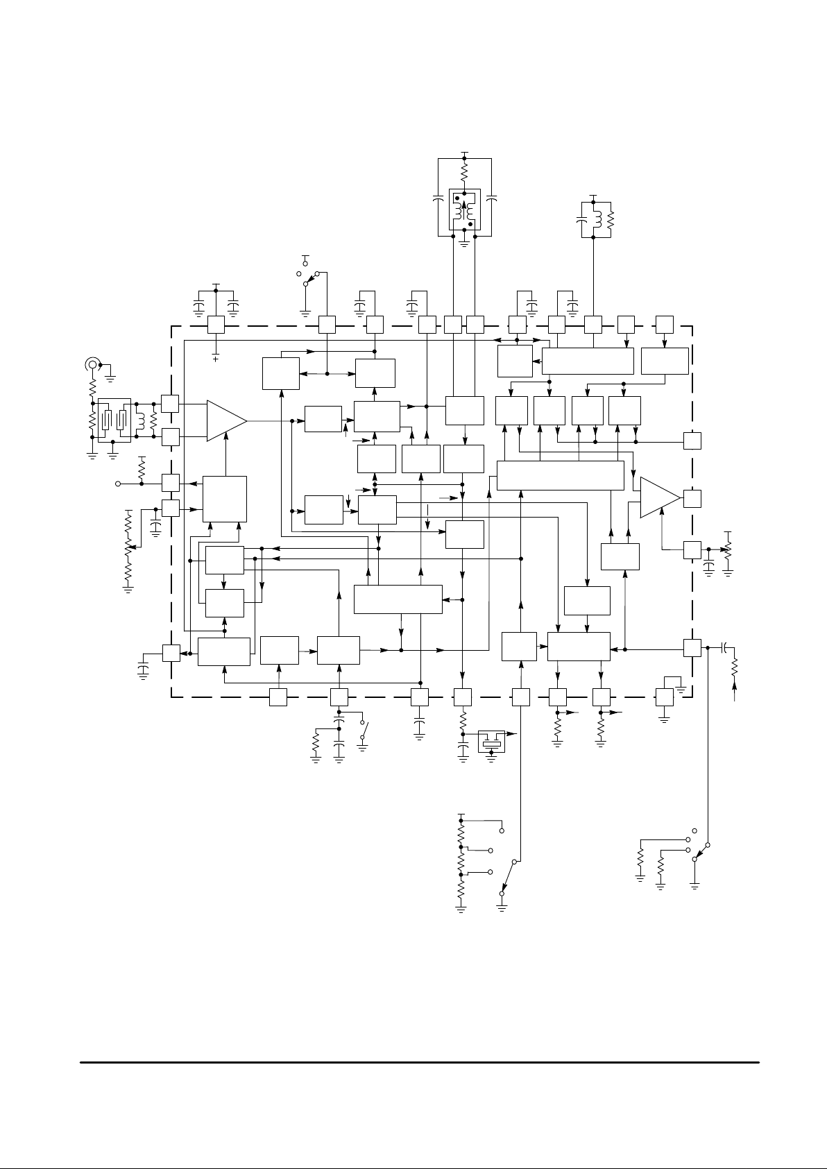
Figure 19. Representative Block Diagram
This device contains 2,641 active transistors.
V
CC
8
9
14
17 16 18 28
10
13
1225 11
15
1
27
24
232267419 2120
2256
Sound
AFT Filter/
Peak
White Filter
Sound
De–
Emphasis
(FM)
AM IF &
Detector
FM IF & Detector
Switch
4
Switch
3
Switch
2
Switch
1
VCO
FM
AFT
V
CC
V
CC
V
CC
V
CC
V
CC
V
CC
V
CC
Gnd
(Pos)(Neg)
Video
Mode
Switch
From
External
Audio
Source
Audio 1
Audio 2
Video 1 Video 2
NTSC
SECAM
PAL 2
PAL 1
Intercarrier
Sound Output
Lock Detector/
Filter
(Acquisition Circuit)
Horizontal PLL Filter
Flyback/
Video Input
Video Invert
Switch
Mode
Switch
Phase
Detector
AFT
Amp
AFT
Clamp
AFT
Switch
Limiter
AGC
Control
Circuit
Limiter
VCO
Sweep
Freq
Doubler
Control
Logic
Audio
Switch
White
Spot Inv
Sound
Q Det
Video 1
Det
Phase
Shift 90
°
Acquisition
Circuit
Horiz PLL
OSC
Sync
Sep
AGC
Discharge
Peak
AGC
Gated
AGC
AFT
Output
PLL Filter
(Main VCO Loop)
IF Input
RF AGC
Output
RF
AGC
Delay
AGC
Filter
Volume
Control
Audio Output
(Variable)
Audio Output
(Constant)
Audio Input/
Audio–Video
Switch
Sound Inputs
(AM)(FM)
Sound
Quadrature
Coil (FM)
VCO
Coil
3
90
°
IF
Amp
Vol
Control
Video Outputs
0
°
90
°
Page 9

MC44302A
9
MOTOROLA ANALOG IC DEVICE DATA
FUNCTIONAL DESCRIPTION
Introduction
The MC44302A is an advanced high performance
multistandard IF system specifically designed for use with all
of the world’s major television modulation techniques
including NTSC, PAL, and SECAM. This device performs the
function of intermediate frequency (IF) amplification,
automatic gain control (AGC), automatic frequency tuning
(AFT) and signal demodulation for transmitting systems that
use either positive or negative amplitude modulated video
along with frequency modulated (FM) or amplitude
modulated (AM) sound. The television designer is offered a
new level of circuit simplicity along with enhanced system
performance when compared to present day television IF
amplifiers. Numerous unique design techniques are
incorporated resulting in only a single tuned circuit
adjustment for a completely aligned video and sound IF
system with tuner AFT output. Special design attention was
given to enhance noise performance and to reduce
differential gain and phase distortion. Additional internal
circuitry is provided to meet the European Peritel socket
requirements along with a means for descrambling video
signals that use either or both amplitude modulated sync and
alternate line video inversion. A detailed block diagram of the
internal architecture is shown in Figure 19 and an operating
description of the major circuit blocks is given below.
IF Amplifier and AGC
The IF amplifier consists of four cascaded ac coupled gain
stages yielding an input sensitivity of 40 µV for a full video
output swing of 2.2 Vpp. This level of sensitivity allows the
use of a single IF block filter without incurring the additional
cost of a preamplifier. A quite acceptable level of signal to
noise performance is achievable by utilizing a tuner with a
gain of 33 dB to 36 dB combined with a low insertion loss
(≤18 dB) surface acoustic wave (SAW) or passive block filter.
The first three stages of the IF amplifier are gain controlled to
provide an AGC range of 80 dB. This extended AGC range
enhances the signal handling capability, resulting in superior
differential phase and gain performance with a significant
reduction of intermodulation products. AGC of the first stage
is internally delayed so as to preserve the amplifier’s low
noise figure characteristics.
An on–chip sync separator and horizontal phase–locked
loop oscillator is provided for noise immune AGC gating in
self contained applications where a horizontal scan signal
may not be available. A positive going sync source connected
to the Flyback/Video input at Pin 17 is used to lock the PLL
and generate an internal AGC keying pulse. The sync
separator allows direct use of the Negative Video output at
Pin 5 as a source for the keying pulse. If horizontal scan
circuitry is available, a positive going flyback pulse can also
be used to set the keying pulse.
A video signal and a reference level are required to
implement automatic gain control of the lF and tuner. The
video AGC reference is selected for a specific modulation
standard by the Video Mode Switch voltage setting at Pin 10;
refer to Table 2. With PAL 1, PAL 2, or NTSC mode selected,
a black level reference is established by AGC keying during
the tip of sync. With SECAM mode selected, a black level
reference is established by AGC keying during the back
porch. In order to correct for the inconsistent back porch level
that is common between SECAM transmitters, a long time
constant non–keyed peak white reference level is also
established, and is used in conjunction with the black level
reference to control the video output level. The peak white
level is used in effect to slowly readjust the black level
reference threshold over a limited range of ±10%. With this
dual reference approach, the accuracy associated with a
typical peak white detecting system is maintained without the
usual sacrifice of speed, thus allowing a quick AGC response
to airplane flutter and channel changes.
The tuner AGC control function consists of an RF AGC
delay adjustment at Pin 15 and an RF AGC output at Pin 13.
The delay adjustment sets the threshold where tuner gain
reduction is to begin. This usually corresponds to a signal
level of 1.0 mV to 2.0 mV at antenna input. The AGC output
is designed to control a reverse AGC type of tuner. As the
antenna signal level increases, the voltage at Pin 13
decreases, causing a gain reduction in the tuner. Since
Pin 13 is an NPN open collector output, an external pull–up
resistor must be added if one is not provided in the tuner.
Pin 13 is guaranteed to sink a minimum of 1.0 mA. Note that
when operating with a tuner that requires in excess of 5.6 V,
current will flow into Pin 13 due to conduction of the upper
internal clamp diode.
Carrier Regeneration
Carrier regeneration is attained by the use of a
phase–locked loop, thus enabling true synchronous
demodulation to be achieved with all of its advantages.
Following the IF amplifier and preceding the PLL phase
detector is a limiting amplifier designed to remove the
amplitude modulation that is present on the carrier. The
amplifier consists of two cascaded differential stages with
direct coupled feedback to set a closed loop gain of 40 dB.
This two stage approach has several distinct advantages
when compared to conventional integrated demodulators
that utilize a single stage limiter. With a two stage limiter, the
gain requirement to remove the video amplitude modulation
can be designed–in without the large voltage swings that are
required by a single stage limiter with equivalent gain. The
large voltage swings lead to poor differential phase and gain
performance, and consequently the need for an external
tuned circuit with two cross coupled limiting diodes. Use of
direct coupled feedback diminishes the effects of the
amplifier’s input offset voltage which can be an additional
source for differential phase and gain errors. The
combination of low voltage swing per stage with dc feedback
eliminates the need for a tuned circuit at the output of the
limiter. This results in a significant component and alignment
cost savings as well as removing the necessity to pin out a
high level IF signal. This high level signal is a potential
radiation source that can result in IF instability at low signal
levels. The only problem of using the two stage limiter is the
potential for an additional static phase shift which will result in
a change of the demodulating angles at both the video and
sound demodulators inputs. This problem is solved by
placing an identical two stage limiter between the frequency
doubler output and the phase detector input. This adds an
identical amount of static phase shift to bring the
demodulating angles back to 0° and 90°.
Page 10

MC44302A
10
MOTOROLA ANALOG IC DEVICE DATA
Figure 20. Phase Detector
2∆I
I +
∆
I
I –
∆
I
I –
∆
I
I +
∆
I
19
Q2
Q1
SW2
VCO
V
CC
SW1
1.0 MHz
Square
Wave
Regenerated
Carrier
(Limited)
1.0 MHz
Square
Wave
SW3
IF Carrier
Signal
(Limited)
Q3
PLL
Filter
Q4
Phase errors, resulting in quadrature video distortion, can
also be caused by dc errors in the phase detector and AFT
amplifier. Most of the dc of fsets are caused by mismatches in
the current mirrors of the push–pull output stage, refer to
Figure 20. Switches SW1, SW2, and SW3 are driven by a
1.0 MHz square wave with an accurate 1:1 mark/space ratio.
Switches SW1 and SW2 maintain the same sense of error
signal, while SW2 ensures errors due to the top PNP current
mirrors average to zero on the external loop filter capacitor. In
a similar way, SW3 by interchanging Q3 and Q4, cancels
errors due to the bottom NPN mirror. With phase errors
reduced to a minimum, there is no need for any external
phase adjustments. The phase detector output is filtered and
it is used to control the VCO in a corrective manner. When the
PLL establishes a locked condition, there will be a 90° phase
shift between the two phase detector inputs.
The Voltage Controlled Oscillator and Frequency Doubler
circuits are shown in Figure 21. The oscillator operates at
one half of the picture carrier frequency and is tuned by a
control bias that is applied to the reactance stage input.
Reactance tuning allows a higher Q to be maintained in the
tank circuit as opposed to a phase shift type of oscillator with
the same tuning range. The oscillator frequency is internally
doubled to picture carrier frequency by a balanced multiplier .
Note that the multiplier input signals are at 90° to each other
for frequency doubling.
Since the oscillator operates at one half of the picture
carrier frequency, radiation from the external tuned circuit
components will not desensitize the system, even if picked
up by the amplifier input leads. This significantly reduces the
possibility of a PLL push–off condition. Running the oscillator
at twice the picture carrier and dividing it down is another way
of solving the IF input radiation problem, but there are two
significant disadvantages. First and foremost, radiation into
the antenna now becomes a problem. In the U.S.A. twice the
picture carrier falls directly into the passband of channel 6,
producing a very noticeable beat. Any second order
harmonics, four times picture carrier, will fall into the
passband of channel 8. Second, it is more difficult to produce
a stable oscillator that operates at twice the IF frequency than
one that operates at one half of the IF frequency.
Figure 21. VCO and Frequency Doubler
Bias
4.7 k
21
Control
Bias
Oscillator
(f
OSC
= 0.5 Pix Carrier)
Reactance
Tuning Stage
Frequency Doubler
Balanced Multiplier
20
V
CC
PLL Limiter for
Video/Sound
Demodulations
(f = Pix Carrier)
Page 11

MC44302A
11
MOTOROLA ANALOG IC DEVICE DATA
Video and Sound Intercarrier Demodulation
To ensure that the above performance improvements
were not lost elsewhere, great care was taken with the
design of the video demodulator and video amplifiers. One
example is in the architectural placement of the phase shift
amplifier (Figure 22) that is required for video demodulation.
This amplifier was placed in series with the IF signal side of
the demodulator, instead of the oscillator side as is common
practice. The 90° phase shift is obtained by a capacitively
coupling each of the differential amplifier driver emitters to
the video demodulator inputs. This results in an output
current that is at 90° with respect to the input voltage over a
wide range of frequencies. Small phase errors that are
caused by the transistor dynamic small–signal emitter
resistance are corrected with the use of cross–coupled
emitter resistors. This arrangement leads to a simpler design
with the ability to tailor the demodulation angle for the lowest
possible distortion at the IF/demodulator interface. The
dynamic emitter resistances, which can give rise to distortion,
are now in quadrature with the capacitive reactance and
therefore contribute very little to the resultant output.
After the PLL attains phase–lock, video and sound
demodulation is obtained by the use of two separate double
balanced multipliers. Video demodulation is accomplished by
multiplying the non–limited 90° phase shifted carrier signal,
with the regenerated vision carrier that is obtained from the
Frequency Doubler output. Both positive and negative video
outputs are produced. The phase relationship between the
video demodulator inputs is 0° since the carrier signal is
phase shifted 90°. This is done in order to cancel out the 90°
phase shift that is present at the inputs of the Phase Detector
when it is locked. The sound intercarrier signal is also
recovered by a multiplier in a similar manner to that of the
video. In this case the carrier signal is not phase shifted, and
the phase relationship between the sound demodulator
inputs is 90°. A consequence of this phase relationship is that
only the higher frequency video components are
demodulated while the lower frequency components, those
that fall within the vestigial sideband, are suppressed. With
negative polarity modulation systems, a significant reduction
in the level of white character sound buzz and hum is
achieved. This is most noticeable when demodulating video
signals that contain a high luma level which can cause the
modulation index to exceed 100 percent.
Figure 22. 90° Phase Shift Amplifier
V
ref
I
out
+
+V
in
I
out
+
–V
in
Video Outputs
Each of the video outputs are part of a wide bandwidth
operational amplifier with internal dc feedback and frequency
compensation. The AGC reference provides the same
composite video output level of approximately 2.2 Vpp for
both positive and negative polarities of video modulation. The
positive video output appears at Pin 6 and is intended to drive
the luma and chroma channels. This output contains a White
Spot Inverter that is used to invert and clamp any
demodulated noise that is significantly above the white level.
This effectively removes the whiter than white noise
produced by the true synchronous demodulator and prevents
the CRT from being overdriven and defocused. The white
spot inversion threshold and clamp levels are set to
approximately 4.0 V and 2.5 V respectively. The negative
video output appears at Pin 5 and is intended to be used as
a sync separator source. With a simple preseparator low
pass noise filter, this output will provide optimum sync
performance. The video outputs are designed to drive a
resistive load that is in the range of 2.0 kΩ. Lower resistance
values could increase differential phase and gain distortion.
Figure 23. Positive Video Output with
White Spot Inversion
White Spot Inversion Threshold
White Spot Clamp Level
4.0 V
3.7 V
2.5 V
1.2 V
Normal
0% and
100%
Carrier
Levels
AM & FM Sound IF and Detection
The intercarrier sound that is present at Pin 28 normally
connects through a ceramic bandpass filter to either the FM
IF and Detector input at Pin 2, or the AM IF and Detector
input at Pin 23. With the FM IF , intercarrier sound is limited by
a five stage ac coupled amplifier yielding high sensitivity and
a high level of AM rejection. The typical limiting threshold is
80 µV, and the AM rejection ratio is in excess of 50 dB. FM
detection is accomplished by a self tuning quadrature
demodulator. An internal reactance stage with phase
compensation is controlled to automatically adjust the tuning
of an external tank circuit eliminating the need for manual
alignment. The tank is a parallel circuit consisting of a fixed
value inductor, capacitor, and resistor. The tuning range is
controlled by the ratio of the internal capacitance change to
that of the fixed external tank capacitance. The internal
capacitance is controlled by the voltage present on the
Sound AFT Filter, Pin 7. The capacitance ranges from
0.25 pF to 19 pF, refer to Figure 9. Figure 10 shows the self
tuning frequency range for three inductor values. In general,
for fixed frequency applications, the external tank
capacitance should be in the range of 56 pF to 82 pF. This
should allow sufficient tuning range to account for the
component tolerances. The L–C values should be selected
so that the AFT filter operates below 2.4 V when properly
tuned to the sound intercarrier. This yields the best low signal
lock–in performance, since the AFT filter voltage approaches
1.0 V under no signal conditions. Multi–standard applications
that require a wide intercarrier tuning range can be
accomplished by using a small external capacitance with a
Page 12

MC44302A
12
MOTOROLA ANALOG IC DEVICE DATA
large inductance. Parasitic layout and coil capacitance must
be considered for optimum performance. Suggested
component values are given in Table 3.
The sound AFT time constant is set by an external
capacitor that is connected from Pin 7 to ground. This
capacitor is driven by an internal 300 µA current source and
sink. The demodulated sound bandwidth is in excess of
100 kHz making this device well suited for MTS
(multi–channel television sound) stereo and SAP (second
audio program) TV applications. Sound de–emphasis is
controlled by the time constant of an internal 18 kΩ resistor
and an external capacitor that is connected from Pin 4 to
ground. The FM IF is active in PAL 1, PAL 2 and NTSC
modes, and provides 2.0 Vpp of audio at the Variable and
Constant outputs.
With the AM IF, intercarrier sound is amplified and
detected by a fully balanced exalted carrier demodulator. The
detector provides in excess of 2.0 Vpp recovered audio
output at Pin 24. An internal low pass filter is incorporated to
suppress any high frequency harmonics that may be present
at the demodulator output. The AM IF is active in both the
SECAM and NTSC modes.
Audio Input/ Audio–Video Switch
The Audio Input/Audio–Video Switch is a multifunction
input that selects the source for the audio that appears at
Pin 27, and the polarity of the video that appears at Pins 5
and 6. There are four possible modes for this input and they
are each selected by applying a specific dc voltage level to
Pin 3. Refer to Table 1 and to the circuit description for Pin 3
in Table 3. Audio 1 is intended for applications where
internally demodulated audio is present at the Variable and
Constant outputs. The Variable output can be used internal to
the TV chassis and the Constant output can be connected to
a jack for earphone or recorder use. Audio 1 is selected by
not having a dc path from Pin 3 to ground. Internally
demodulated audio (AM or FM) will appear at Pins 24 and 27,
negative video at Pin 5, and positive video at Pin 6. If there is
an ac coupled audio source present at Pin 3, it will be
internally disconnected. Audio 2 is intended for European
applications where internal and external audio sources must
be routed through the Peritel socket. Internally demodulated
audio present at the Constant output can be routed out the
Peritel socket while external audio can be routed in, ac
coupled to Pin 3, and level adjusted at Pin 1 for use within the
TV chassis. Audio 2 is selected by connecting a 22 kΩ
resistor from Pin 3 to ground. Internally demodulated audio
(AM or FM) appears at Pin 24, negative video at Pin 5,
positive video at Pin 6, and the ac coupled external audio
source at Pin 3 appears at Pin 27 inverted. The audio level
into Pin 3 must be limited so that the selected mode of
operation is not changed during the peak excursions with
Audio 2 selected, and the valley excursion with Audio 1
selected. With the component values shown in Table 3, the
audio level should be limited to less than 1.1 Vrms. Video 1
and 2 modes provide a simple means to recover scrambled
video in systems that use some form of alternate line video
inversion. Descrambling is accomplished by switching
between the two video modes. Video 1 is selected by
connecting a 3.3 kΩ resistor from Pin 3 to ground. Internally
demodulated audio (AM or FM) will appear at Pins 24 and 27,
negative video at Pin 5, and positive video at Pin 6. Video 2 is
enabled when Pin 3 is grounded, usually by an IC or a
transistor that is gated on alternate or multiple lines. Internally
demodulated audio (AM or FM) appears at Pins 24 and 27,
positive video with white spot inversion at Pin 5, and negative
video at Pin 6. Note that Video 1 mode is identical to Audio 1.
Video 1 is provided so that when descrambling, Pin 3 does
not have to pass through the voltage range that selects
Audio 2. This prevents unwanted switching noise and buzz
from appearing at the audio outputs.
It should be noted that when combining the features of
Pin 3 with the Peritel socket, the TV chassis can provide the
audio and video source to drive an external monitor or video
recorder. Also an externally generated audio and video
source can be used to drive the TV chassis as a monitor.
DC Volume Control
The dc volume control consists of an electronically
controlled audio amplifier that has a range of 12 dB gain, to
60 dB attenuation. The audio output level is set by applying a
control voltage to Pin 1. This can be derived from an
electronic source such as a digital to analog converter, or a
manual source such as the wiper of a potentiometer that is
connected from VCC to ground. The potentiometer should be
20 kΩ or less. Because no audio signal is present on Pin 1,
any potential for hum and noise pickup can easily be
bypassed by connecting a capacitor from this pin to ground.
In most cases, an unshielded wire or printed circuit board
trace is all that is required to connect the variable voltage
source to the IF board.
Page 13

MC44302A
13
MOTOROLA ANALOG IC DEVICE DATA
Table 1. Audio Input/Audio–Video Switch
Outputs
Inputs
to Pin 3
Audio
1
Video
Mode
AC Signal
DC Level
(V
CC
= 5.0 V)
Constant
Pin 24
Variable
2
Pin 27
Negative
Pin 5
Positive
Pin 6
ÁÁ
Á
ÁÁ
Audio 1
ÁÁ
Á
ÁÁ
External
Audio
БББББ
Á
БББББ
Open
or
3.4 V to 5.0 V
ÁÁÁÁ
Á
ÁÁÁÁ
Internal Audio
(AM or FM)
ÁÁÁ
Á
ÁÁÁ
Internal Audio
(AM or FM)
БББББ
Á
БББББ
Negative Video
БББББ
Á
БББББ
Positive Video
with
White Spot Inversion
ÁÁ
Á
ÁÁ
Á
Audio 2
ÁÁ
Á
ÁÁ
Á
External
Audio
БББББ
Á
БББББ
Á
22 kΩ to Ground
or
1.8 V to 2.2 V
ÁÁÁÁ
Á
ÁÁÁÁ
Á
Internal Audio
(AM or FM)
ÁÁÁ
Á
ÁÁÁ
Á
External Audio
БББББ
Á
БББББ
Á
Negative Video
БББББ
Á
БББББ
Á
Positive Video
with
White Spot Inversion
ÁÁ
Á
Video 1
ÁÁ
Á
–
БББББ
Á
3.3 kΩ to Ground
or
0.6 V to 0.9 V
ÁÁÁÁ
Á
Internal Audio
(AM or FM)
ÁÁÁ
Á
Internal Audio
(AM or FM)
БББББ
Á
Negative Video
БББББ
Á
Positive Video
with
White Spot Inversion
ÁÁ
Á
Video 2
ÁÁ
Á
–
БББББ
Á
Grounded
or
0 V to 0.03 V
ÁÁÁÁ
Á
Internal Audio
(AM or FM)
ÁÁÁ
Á
Internal Audio
(AM or FM)
БББББ
Á
Positive Video
with
White Spot Inversion
БББББ
Á
Negative Video
ББББББББББББББББББББББББББББББББ
Á
NOTES: 1. Refer to T able 2 to determine the active demodulator (AM and or FM) and the associated audio output pins.
2.The Variable output audio level is controlled by Pin 1.
Table 2. Television Standard Modes
Television Standard
БББББББ
Mode Selection
AGC
Sound
Video
ÁÁÁÁ
Pin 10
Pin 16
Reference
Time
IF and
Modulation
Audio
System
Modulation
Polarity
ÁÁÁÁ
Voltage
(V)
DC
Loading
and
Method
Constant
Pin #
Active
Inhibited
Output
Pin #
ÁÁ
Á
PAL 1
ÁÁÁÁ
Á
Negative
ÁÁÁÁ
ÁÁÁ
Á
4.0 to 5.0
ÁÁ
Á
Open
БББББ
Á
Black Level
Sync Tip Keyed
ÁÁÁ
Á
14
ÁÁ
Á
FM
ÁÁ
Á
AM
ÁÁ
Á
24, FM
27, FM
ÁÁ
Á
PAL 2
ÁÁÁÁ
Á
Negative
ÁÁÁÁ
ÁÁÁ
Á
3.2 to 4.0
ÁÁ
Á
Open
БББББ
Á
Black Level
Sync Tip Keyed
ÁÁÁ
Á
14
ÁÁ
Á
FM
ÁÁ
Á
AM
ÁÁ
Á
24, FM
27, FM
ÁÁ
Á
ÁÁ
Á
SECAM
ÁÁÁÁ
Á
ÁÁÁÁ
Á
Positive
ÁÁÁÁ
ÁÁÁ
Á
ÁÁÁ
Á
1.9 to 3.0
ÁÁ
Á
ÁÁ
Á
Open
БББББ
Á
БББББ
Á
Black Level
Back Porch Keyed
White Level
Peak Detected Video
ÁÁÁ
Á
ÁÁÁ
Á
14
7
ÁÁ
Á
ÁÁ
Á
AM
ÁÁ
Á
ÁÁ
Á
FM
ÁÁ
Á
ÁÁ
Á
24, AM
27, AM
NTSC
Negative
ÁÁÁÁ
Ground
Open
Black Level
Sync Tip Keyed
14
AM & FM
–
24, AM
27, FM
Multi–Standard Operating Modes
The MC44302A is designed to operate properly with PAL
(B, G, I,) SECAM (L), and NTSC (M) television transmission
standards. There are two multifunction inputs that are used
to select the proper control methods for video
demodulation, sound intercarrier demodulation, and AGC.
This keeps the sense of the video signal at the outputs the
same, whether positive or negative modulation is being
received. Refer to Table 2 and the following operating
description.
The PAL, NTSC, and SECAM standard are each selected
by applying a specific dc voltage level to the Video Mode
Switch at Pin 10. With PAL 1 selected, AGC is keyed on the
sync pulse by the horizontal PLL which is locked to the
flyback or video sync pulse present at Pin 17. The FM sound
IF and detector is active with the demodulated audio
appearing at Pins 24 and 27. The P AL 2 selection is identical
to PAL 1 with the addition of sound muting when the
Acquisition Circuit is unlocked or vertical sync is absent. With
SECAM selected, the video level is established by both, a
long time constant peak white detector, and a back porch
keyed AGC that corrects for transmitted black level errors
while maintaining fast AGC response. The AM sound
detector is active with the demodulated audio appearing at
Pins 24 and 27. With NTSC selected, AGC and sound muting
is the same as for PAL 1 mode. The FM and AM detectors are
both active with the FM output at Pin 27 and the AM output at
Pin 24. The AM output can be used to obtain the sync signal,
in suppressed sync scrambling systems, that is amplitude
modulated on the sound carrier.
Signal Acquisition and AFT
The automatic fine tuning (AFT) portion of this integrated
circuit is unconventional in form. AFT control is derived by
amplifying the phase detector error voltage and applying it to
the tuner local oscillator (LO) after phase lock is established.
This method eliminates the need for a discriminator coil along
with the associated alignment, and the potential for IF
instability due to coil radiation.
Page 14

MC44302A
14
MOTOROLA ANALOG IC DEVICE DATA
The MC44302A is unique in that it uses the VCO loop as a
frequency reference for the tuner AFT loop. After signal
acquisition and phase lock, the VCO and AFT loops will
reach a steady state condition. The VCO will have moved
only a small amount from it’s nominal frequency (∆f
VCO
) with
the tuner local oscillator (∆fLO) correcting for the majority of
the frequency error (∆fe). Therefore in steady state condition
∆fe = ∆f
VCO
+ ∆fLO, and ∆fLO >> ∆f
VCO
. This is due to the
much higher gain in the tuner LO loop when compared to that
of the VCO loop. In this way, the VCO can be used as the
frequency reference for the AFT system provided that the
PLL can be initially locked to the incoming IF signal. This
combination of the tuner LO loop and the VCO loop forms a
double loop PLL system. Analysis shows that the overall
system stability can be assured by treating the VCO loop as
a single stand alone PLL. This is valid if the VCO loop has low
gain and high bandwidth which guarantees initial capture,
while the tuner LO loop has high gain and low bandwidth
which minimizes frequency and phase offsets.
The AFT system is designed to acquire the vision carrier,
without false locking to the sound or adjacent sound carriers,
with an initial tuner LO frequency error of ±2.0 MHz. This
error is reduced to less than ±10 kHz upon establishing
acquisition and after both the VCO loop and tuner AFT loop
have reached their steady state condition. In contrast, the
discriminator coil type of AFT has a highly asymmetric lock
characteristics with a frequency error in the range of about
–2.0 MHz to 1.0 MHz. This large frequency error is due to the
effects of lower loop gain combined with the IF filter slope.
Higher loop gain can be incorporated into the discriminator
coil type of AFT but circuit problems due to large dc offsets,
and IF stability due to coil radiation at the picture carrier
frequency can be difficult to resolve. In order to achieve a
high performance level, without encountering the ill effects
associated with high gain discriminator circuits, a novel
approach to establishing PLL lock up was developed.
Figures 24 and 25 graphically illustrate the Acquisition
Circuit operation. In the absence of an IF signal, the
Acquisition Circuit examines the state of the Video (I) and
Sound (Q) demodulators, detecting that the VCO is out of
lock. On loss of lock, the AFT Output at Pin 11 (tuner LO
drive) is clamped, and the Lock Detector output at Pin 18 is
placed in a sink mode, causing its filter capacitor to
discharge. As the capacitor voltage falls below 3.7 V, the
application of a VCO offset starts and is completed at 3.0 V.
The capacitor voltage will continue to fall stopping at 2.7 V
until the Acquisition Circuit detects a signal. At this point both
the tuner and IF are offset by the same amount from their
nominal frequency of 45.75 MHz. Thus a picture carrier
would now be converted to 43.75 MHz and the Main VCO
Loop voltage at Pin 19 would be centered within its dynamic
range at 3.2 V.
The AFT offset is controlled by the system designer to
approximately –2.0 MHz. This is done so that if a nominal IF
signal appeared, its picture carrier would be centered in the
IF filter passband where there is minimum attenuation. Note
that even if the tuner LO drifts by as much as ±2.0 MHz, the
signal will still not be significantly attenuated.
On the arrival of a signal, beat notes are detected at the
output of the demodulators, and the Lock Detector output is
again placed in a sink mode to further discharge the filter
capacitor. When the capacitor voltage falls below 1.3 V, the
VCO Sweep is initiated at Pin 19. This causes the VCO to be
swept an additional –2.0 MHz from its out of lock nominal
centered IF frequency. During this negative sweep, the PLL
Phase Detector is inhibited so that a phase lock cannot be
obtained. When the capacitor voltage at Pin 19 falls to 2.0 V,
the Phase Detector is made active and the VCO is swept in a
positive direction from –2.0 MHz to 2.0 MHz of the out of lock
centered IF frequency. The PLL will therefore lock to the first
carrier it encounters. This in fact has to be a vision carrier
since the sound carrier is more than 2.0 MHz below the
nominal frequency, and the adjacent lower channel sound
carrier is higher than the vision carrier. PLL lock can occur at
any point during the positive going sweep of Pin 19 from
2.0 V to 4.2 V. On achieving lock, the Lock Detector output is
released allowing the voltage across the filter capacitor to
rise. When this voltage reaches 3.0 V, a gradual removal of
the VCO offset starts. At 3.7 V removal is completed, the
VCO Sweep circuit is inhibited, and the AFT clamp is
removed. The phase detector remains permanently enabled.
Upon removal of the AFT Clamp, the error voltage that
appears at the AFT Amplifier output will drive the incoming
signal towards the nominal IF frequency of 45.75 MHz. The
Main VCO Loop will track the incoming IF signal while
maintaining phase and frequency lock as the loops settle.
This is attainable because the tuner AFT loop response is
slow while the Main VCO loop is fast. For large frequency
errors during this period, the slew rate of the tuner LO loop is
automatically increased but not to the extent where it would
cause a VCO tracking problem. This technique allows the
acquisition time of the circuit to be reduced considerably
while still using a larger than normal time constant in the
tuner LO loop. In this way, any possibility of phase
modulating the LO with video is removed.
The amount of AFT offset is controlled by the output swing
of Pin 11, the voltage to frequency sensitivity of the tuner’s
AFT input, voltage gain or attenuation of any interface level
shifting circuitry, and the alignment accuracy of the VCO coil.
The amount of VCO offset and VCO sweep is controlled by
the change in capacitance ratio of the internal tuning
capacitance to that of the fixed external tank capacitors C19
and C20. To insure proper PLL lock, it is recommended that
the VCO sweep is limited to less than 5.0 MHz and that C19
and C20 are not be less than 33 pF.
Page 15

MC44302A
15
MOTOROLA ANALOG IC DEVICE DATA
Adjacent
Lower Channel
Figure 24. Acquisition Circuit Operation
39.75
Adjacent
Pix Trap
Typical IF Bandpass Filter Response
Properly Tuned Desired Channel
Initial 2.0 MHz VCO with the AFT clamped. Note that
if the Desired Channel picture carrier appears, it will
be centered in the IF passband.
When a beat note is detected, the VCO is swept another 2.0 MHz
low with the phase detector is inhibited. The VCO is then swept high
with the phase detector enabled. Upon phase lock, the AFT clamp is
removed, the initial VCO offset is slowly released, and the VCO
Sweep is inhibited. Capture of the desired picture carrier is assured
even if mistuned
±
2.0 MHz.
–2.0 MHz mistuning of the Desired
Channel with an initial 2.0 MHz offset.
2.0 MHz mistuning of the Desired
Channel with an initial 2.0 MHz offset.
Adjacent
Upper Channel
Adjacent
Lower Channel
Adjacent
Upper Channel
Adjacent
Upper Channel
Adjacent
Lower Channel
Adjacent
Upper Channel
Snd Pix
PixSndPixSnd
Snd Pix Snd
Snd PixPixSndPixSnd
Snd
Pix
Phase Detector Inhibited
Desired
Channel
Phase Detector Active
Adjacent
Lower Channel
Desired
Channel
SndPix Pix Snd
Pix Snd
Pix
Desired
Channel
Desired
Channel
41.25 45.7543.75
41.75
47.25
Adjacent
Snd Trap
Carried
Detected
It must be noted that in the operating description of this
device, any reference made to the amount of VCO offset or
sweep is the actual effect on the IF passband. The true VCO
frequency change is only one half of that stated due to the
Frequency Doubler circuit.
The AFT system is designed to control all types of varactor
tuned local oscillators via the AFT Mode Switch input at
Pin 12. This input is used to activate the output of the AFT
control amplifier that appears at Pin 11, and to select the
control voltage polarity versus IF frequency. With the AFT
Mode Switch input connected to VCC, Pin 11 is placed in a
sourcing mode when the IF carrier frequency is below
nominal. With the AFT Mode Switch input grounded, Pin 11 is
placed in a sinking mode when the IF carrier frequency is
below nominal. With the AFT Mode Switch input
disconnected, Pin 1 1 is internally clamped to one half of VCC,
refer to Figures 6 and 25. Under this condition the TV set can
be tuned manually and appear to have a conventional type of
AFT with a smooth capture characteristic. Most other PLL
AFT systems cannot be manually tuned in this manner as
they tend to exhibit an undesirable abrupt capture
characteristic. Digital phase–locked loop tuning systems can
also be controlled with the addition of a varactor diode used
to shift the PLL reference oscillator.
Page 16

MC44302A
16
MOTOROLA ANALOG IC DEVICE DATA
Figure 25. Acquisition Circuit Timing
PLL Lock
4.2 V
3.2 V
2.0 V
4.3 V
3.7 V
3.0 V
2.7 V
1.3 V
0.8 V
4.5 V
2.5 V
0.5 V
PLL Filters
(Main VCO Loop)
Pin 19
Lock Detector/Filter
(Acquisition Circuit)
Pin 18
AFT Output
Pin 11
Signal No
Signal
Signal
Signal
Detection
Completed
VCO Offset
Application
Start
Start
Completed
VCO Offset
Removal
VCO Sweep
Inhibited
Phase
Detector
Inhibited
Phase
Detector
Active
Phase
Detector
Active
Pin 12 = Gnd
Pin 12 = Open
Pin 12 = V
CC
Final Static
Condition
AFT CorrectingAFT ClampedAFT
Static
AFT Static
VCO Sweep
Initiated
fIF High
fIF Nominal
In order to make the above drawing easier to comprehend, the vertical voltage axis was drawn to scale but the horizontal time axis was not. The typical slewing
time for each output with the component values shown in the application circuit is as follows:
PLL Filter (Main VCO Loop) Pin 19 – 3.5 ms total sweep time when discharging down from 4.2 V to 2.0 V and charging back up to 4.2 V.
Lock Detector/Filter (Acquisition Circuit) Pin 18 – 4.0 ms when slewing up from 0.8 V to 4.3 V.
AFT Output Pin 11 – 12 ms when slewing from 4.5 V or 0.5 V to the final static condition of 2.5 V.
Page 17

MC44302A
17
MOTOROLA ANALOG IC DEVICE DATA
Figure 26. Alignment Configuration
Tuner
CW Picture Carrier
V
CC
VCO
Sweep
Limiter
Freq
Doubler
Frequency
Counter
Bandpass
Filter
≈
2.5 V
AFT
Switch
V
CC
8.2 k
VCO
Coil
IF
Amp
Phase
Detector
Limiter
AFT
Clamp
AFT
Amp
VCO
V
CC
V
Local
OSC
Mixer
RF
Amp
9
8
25
12 11 19 20 21
Alignment
Tuning of a single coil is all that is required for complete
alignment of the IF amplifier. This is most easily
accomplished with the test set–up shown in Figure 26. The
tuner is set to a given channel and a CW signal that is
precisely set to the picture carrier frequency of that channel,
is connected to the tuner RF input. The dc power supply is
adjusted until the tuner output, measured by the frequency
counter, is equal to the required IF picture carrier (45.75 MHz
in the USA). The VCO coil is then adjusted so that the voltage
across the 8.2 k resistor approaches zero. A voltage level of
less than 5.0 mV should be easy to attain. The RF signal and
the dc supply are removed and alignment is completed.
The tuning system should be designed so that the required
varactor bias is approximately 2.5 V when phase–locked to
the nominal IF signal. This centers the AFT amplifier’s
current source/sink output, Pin 11, yielding the maximum
compliance voltage for optimum hold–in and pull–in
characteristics. When interfacing Pin 11 with the tuning
system’s control bias, the output current must not exceed
4.0 mA. This current can be limited with the addition of a
series output resistor if the AFT amplifier is required to drive
a low resistance load.
Differential Phase and Sound Buzz
Even with all the care taken in this design, some residual
differential phase still remains. Although small, refer to
Figure 8, it results in an output on the phase detector that
modulates the VCO and the sound intercarrier. This in turn
has the potential of degrading the stereo sound performance.
In addition, there is a quadrature differential phase shift that
is produced by the shape of the IF bandpass filter. Both
produce currents in the output of the phase detector which in
turn phase modulates the VCO. This phase modulation is
imposed on the sound intercarrier resulting in a video related
sound buzz. These currents can be canceled by injecting the
correct amplitude and phase of demodulated video into the
PLL filter. This can be accomplished with the addition of the
differential phase correction circuit shown in Figure 27. The
phase detector current that is due to the in–phase differential
gain is canceled by the resistor current, and the quadrature
component that is induced by the IF filter is canceled by the
capacitor current. With proper adjustment, the differential
phase distortion can be reduced to less than 0.5 degrees as
well as eliminating any perceptible sound buzz. The source
for the demodulated video to be injected into the PLL filter
can be obtained from Pins 5 or 6. This must be determined
experimentally for a given printed circuit board layout in order
to obtain the best results. With the use of the correction
circuit, this system achieves a similar level of performance to
that of a parallel sound IF system.
Electrostatic Protection
Most pins on the IC have electrostatic protection diodes to
VCC and ground. It is therefore imperative that no pin is taken
below ground or above VCC by more than one diode drop,
approximately 0.6 V, without current limiting.
Figure 27. Differential Phase Correction Circuit
5.0–25 pF
From Negative Video Output Pin 5
or Positive Video Output Pin 6
500 k
82 k
0.1
To PLL Filter
(Main VCO Loop)
Pin 19
Page 18

MC44302A
18
MOTOROLA ANALOG IC DEVICE DATA
PIN FUNCTION DESCRIPTION
Pin No. Equivalent Internal Circuit Description
1
1
0.01
VCCV
CC
10 k
V
CC
Volume
Control
DC Volume Control
A potentiometer of 20 kΩ or less, connected as shown, is used to
adjust the audio output level at Pin 27. There is no audio signal
present at this pin, allowing the use of unshielded wire between
the IF board and the potentiometer. To prevent hum and noise
pickup, a bypass capacitor connects from this pin to ground. Refer
to Figure 17.
2
2
From Ceramic Sound
IF Filter at Pin 28
V
CC
2.2 k
V
CC
Sound Input (FM)
Sound Input (FM)
This pin is the input of the FM IF . The intercarrier sound output at
Pin 28 connects to this input through a ceramic bandpass filter.
The FM detector is active in PAL 1, PAL 2, and NTSC modes.
Refer to Table 2.
3
15.5 k
From External
Audio Source
27 k
Audio Input/
Audio–Video
Switch
3
V
CC
Audio 2
Audio 1
Video 1
Video 2
0.1
V
3.3 k
22 k
Audio Input/Audio–Video Switch
This is a multifunction input that selects the audio source that
appears at Pin 27, and the video polarity at Pins 5 and 6. Audio 1
is without a dc path from Pin 3 to ground. Internally demodulated
audio (AM of FM) appears at Pins 24 and 27, negative video at
Pin 5, and positive video at Pin 6. The audio source at Pin 3 is
internally disconnected. Audio 2 is with the 22 kΩ resistor
connected. Internally demodulated audio (AM or FM) appears at
Pin 24, negative video at Pin 5, positive video at Pin 6, and the
audio source at Pin 3 appears at Pin 27. Video 1 is with the 3.3 kΩ
resistor connected. Internally demodulated audio (AM or FM)
appears at Pins 24 and 27, negative video at Pin 5, and positive
video at Pin 6. Video 2 is with Pin 3 grounded. Internally
demodulated audio (AM of FM) appears at Pins 24 and 27,
positive video at Pin 5, and negative video at Pin 6. Refer to
Table 1.
4
4
C4
0.0033
V
CC
Sound De–Emphasis (FM)
V
CC
18 k
200
µ
A
100
µ
A
Sound De–Emphasis (FM)
A capacitor is connected from this pin to ground. It is used in
conjunction with internal 18 kΩ resistor to set the FM sound
de–emphasis time constant. The typical de–emphasis time
constant required for a flat audio response is 75 µs in the United
States and 50 µs in Europe. The FM sound detector frequency
response for different de–emphasis capacitor values is shown in
Figure 12.
Page 19

MC44302A
19
MOTOROLA ANALOG IC DEVICE DATA
PIN FUNCTION DESCRIPTION (continued)
Pin No. DescriptionEquivalent Internal Circuit
5
V
CC
Negative Video Output
V
CC
60
1.0 mA
2.0 k
6
3.4
1.2
Negative Video Output
Negative going video appears at this output and it is intended to
drive a sync separator. Positive going video will appear at this
output when Pin 3 is grounded. This feature provides a simple
means for descrambling the video signal in systems that use
alternate line video inversion. Refer to the description of Pin 3. The
video output is designed to drive a resistive load that is in the range
of 2.0 kΩ. Lower resistance values will tend to increase output
distortion.
6
V
CC
Positive Video Output
V
CC
60
1.0 mA
2.0 k
6
3.4
1.2
Positive Video Output
Positive going video appears at this output and is intended to drive
the luma and chroma channels. Negative going video will appear
at this output when Pin 3 is grounded. This feature provides a
simple means for descrambling the video signal in systems that
use alternate line video inversion. Refer to the description of Pin 3.
The positive going video signal always contains white spot
inversion whether it appears at output Pins 5 or 6. The video
output is designed to drive a resistive load that is in the range of
2.0 kΩ. Lower resistance values could increase output distortion.
7
7
Sound AFT Filter/
Peak White Filter
V
CC
V
CC
0 to
±
300 µA
10
V
CC
SECAMPAL
NTSC
Sound AFT Filter/Peak White Filter
A capacitor connected from this pin to ground is used to adjust the
sound AFT time constant in PAL and NTSC modes, and video
peak white AGC time constant in SECAM mode. The sound AFT
filter voltage controls the internal tuning capacitance that is placed
across the sound quadrature coil at Pin 26. Refer to Figure 9.
8, 9
Video IF
Input
V
CC
8
3.4 k
9
Video IF Input
These pins are the inputs to the video IF amplifier. The amplifier
consists of four ac coupled stages with an input sensitivity of
40 µV for a 2.2 Vpp video output swing. This sensitivity eliminates
the need for a preamplifier when used with suitable surface
acoustic waves or passive block filters. The IF block filter must be
located close to the IC package inputs to prevent unwanted pickup
and possible instability problems. The input lead lengths must be
kept short with a symmetrical printed circuit board layout.
Page 20

MC44302A
20
MOTOROLA ANALOG IC DEVICE DATA
PIN FUNCTION DESCRIPTION (continued)
Pin No. DescriptionEquivalent Internal Circuit
10
Video Mode Switch
3.0 k
V
CC
V1
V2
V
CC
2.4 k
5.1 k
PAL 1
PAL 2
SECAM
NTSC
10
Video Mode Switch
A dc voltage at this input selects the proper video AGC and sound
demodulation technique for PAL, SECAM, and NTSC. With PAL
1 selected, AGC is keyed on the sync pulse by the horizontal PLL
which is locked to the flyback or video sync pulse present at Pin 17.
The FM sound IF and detector is active. The PAL 2 selection is
identical to PAL 1 with the addition of sound muting when the
acquisition circuit is unlocked or vertical sync is absent. With
SECAM selected, the video level is established by both, a long
time constant peak white detector , and a back porch keyed AGC
that corrects for transmitted black level errors while maintaining
fast AGC response. The AM sound detector is active. With NTSC
selected, AGC and sound muting is the same as in PAL 1 mode.
The FM and AM detectors are both active with the FM output at
Pin 27 and the AM output at Pin 24. Refer to Table 2.
11
11
AFT Ouput
V
CC
3.3
V
CC
Digital Slew
Rate Control
To Tuner AFT Input.
IO must be externally
limited < 4.0 mA.
0 to ±500 µA
or
±
2.0 mA
Variable
Reference
Clamp Voltage
20
AFT Output
With detent type tuners, the automatic fine tuning output can be
used to directly control the tuner local oscillator varactor. The
varactor control input must be high impedance in order to maintain
high AFT loop gain with acceptable dynamic response. This
output has a linear sink and source current range of 0 to 500 µA,
and is digitally switched to ±2.0 mA for large frequency errors. The
capacitor from Pin 11 to ground limits the bandwidth of the tuner
local oscillator loop. Digital phase–locked loop tuning systems
can also be controlled with the addition of a varactor diode used
to shift the PLL reference oscillator . Refer to Figures 6, 24, and 25.
12
AFT Mode Switch
V
CC
V
CC
V
CC
12
24 k
24 k
5.1 k
AFT Mode Switch
This input is used to activate the output of the AFT control amplifier
that appears at Pin 11, and to select the control voltage polarity
versus IF frequency. This feature allows the AFT output to work
with all types of varactor tuned local oscillators. With the AFT
Mode Switch input connected to VCC, Pin 11 is placed in a
sourcing mode when the IF carrier frequency is below nominal.
With the AFT Mode Switch input grounded, Pin 11 is placed in a
sinking mode when the IF carrier frequency is below nominal. With
the AFT Mode Switch input disconnected, Pin 11 is internally
clamped to one half of VCC, refer to Figures 6 and 25.
13
V
CC
V
CC
V
CC
RF AGC
Output
10 k
To Tuner
AGC Input
13
RF AGC Output
This output is designed to control a reverse AGC tuner. As the
antenna signal level increases, the voltage at Pin 13 decreases,
causing a gain reduction in the tuner RF stage. An external pull–up
resistor must be added if one is not provided in the tuner. Pin 13
is guaranteed to sink a minimum of 1.0 mA. Note that when
operating with a tuner that requires in excess of 5.6 V , current will
flow into Pin 13 due to conduction of the upper internal clamp
diode.
Page 21

MC44302A
21
MOTOROLA ANALOG IC DEVICE DATA
PIN FUNCTION DESCRIPTION (continued)
Pin No. DescriptionEquivalent Internal Circuit
14
V
CC
V
CC
Video IF
AGC Filter
0.1
14
Horizontal
Gating
2.0 V
Video IF AGC Filter
A capacitor connects from this pin to ground to control the video
IF AGC rate of change with respect to a change in input signal
level. An increase in input signal level causes an increase in the
voltage at Pin 14 which controls the internal AGC action. Pin 14
has an unsymmetrical source and sink current of 150 µA and 8.0 µA
respectively. The AGC filter voltage versus IF differential input
signal level is shown in Figure 1.
15
6.2 k
V
CC
1.0 k
4.3 k
RF AGC
Delay
From Pin 14
AGC Filter
Voltage
0.01
15
V
CC
V
CC
Internal
IF AGC
RF AGC Delay
A voltage applied to this input sets the video IF signal level
threshold before gain reduction of the tuner begins. The threshold
setting is tuner dependent but is usually in the range of 1.0 mV to
2.0 mV of signal at the antenna. Too low of a setting will cause
premature tuner gain reduction and a poor picture and sound
signal to noise ratio, while too high of a setting will cause tuner
overload and picture distortion. The IF differential input signal
level versus RF AGC takeover threshold is shown in Figure 2.
16
16
Horizontal PLL Filter
0.05
0.68
1.5 k
V
CC
V
CC
0.4 mA
0.4 mA
Horizontal PLL Filter
This is a dual function pin. With the network shown, the horizontal
phase–locked loop oscillator provides a keying pulse to properly
gate the AGC when in PAL, SECAM, and NTSC modes. With
Pin 16 grounded, both the AM and FM sound IF and detectors are
inhibited. By placing Pin 3 in the Audio 2 mode, the variable audio
output at Pin 27 is active and can be used to control the level of
the externally processed digital sound. Refer to the description of
Pin 3.
Page 22

MC44302A
22
MOTOROLA ANALOG IC DEVICE DATA
PIN FUNCTION DESCRIPTION (continued)
Pin No. DescriptionEquivalent Internal Circuit
17
Flyback/Video Input
17
0.02
V
CC
V
CC
From Negative Video
Output Pin 5
Flyback/Video Input
This input connects to a positive going sync source to generate an
internal AGC keying pulse. An internal sync separator is provided
for use in stand alone applications where a horizontal scan signal
is unavailable. The sync separator allows direct use of the
negative video output at Pin 5 to set the internal keying pulse. If
horizontal scan circuitry is available, a positive going flyback pulse
can be used instead to set the keying pulse.
18
Lock Detector/Filter
(Acquisition Circuit)
18
V
CC
V
CC
0.1
V
CC
0 or
±80 µ
A
5.0 k
3.3 V
68 k
Lock Detector/Filter (Acquisition Circuit)
A filter capacitor for the acquisition circuit lock detector connects
from this pin to ground. The capacitor voltage will vary upon signal
presence and lock condition. Typical voltages are 2.7 V with the
circuit unlocked and without any signal, 0.8 V to 4.3 V during signal
acquisition, and 4.3 V when locked. Refer to the Acquisition Circuit
Timing in Figure 25.
19
PLL Filter (Main Loop)
19
V
CC
V
CC
3.9 V
220
0.10.01
V
CC
22 k
0 to ±160 µA
PLL Filter (Main VCO Loop)
A filter capacitor for the main phase–locked loop circuit connects
from this pin to ground. The typical capacitor voltage is 3.2 V when
locked and the circuit has reached the final static condition. Refer
to Figure 5 for the PLL filter voltage versus carrier frequency
change, and to Figure 25 for the acquisition circuit timing.
20, 21
V
CC
V
CC
C20
C19
VCO CoilVCO Coil
V
CC
560
L4
2120
4.7 k4.7 k
VCO Coil
These are the voltage controlled oscillator pins. Symmetrical
tuning about the VCO frequency is provided by a bifiliar wound coil
that resonates at one half of the desired IF frequency. The coil
must be placed close to the IC pins to prevent any unwanted
pickup or radiation. The printed circuit board layout must have
short symmetrical traces with adequate grounding for the can
shield. Capacitors C19 and C20 should not be less than 33 pF.
Suggested component values for the major IF frequencies are
listed in Table 3.
Page 23

MC44302A
23
MOTOROLA ANALOG IC DEVICE DATA
PIN FUNCTION DESCRIPTION (continued)
Pin No. DescriptionEquivalent Internal Circuit
22
Gnd
22
Gnd
This pin is the internal circuit ground. Care must be taken with the
printed circuit board layout to provide a continuous sea of copper
around the IC.
23
V
CC
5.5 k
V
CC
Sound Input (AM)
23
From Ceramic Sound
IF Filter at Pin 28
Sound Input (AM)
This pin is the input of the AM IF . The intercarrier sound output at
Pin 28 connects to this input through a ceramic bandpass filter.
The AM detector is active in SECAM and NTSC modes. Refer to
Table 2.
24
V
CC
V
CC
Audio Output
(Constant)
24
200
1.0 mA
Audio Output (Constant)
This is the constant audio output. The audio source is controlled
by the mode selection of Pin 3. Refer to the description of Pin 3,
and to Tables 1 and 2.
25
330 0.01
V
CC
25
5.0 V
V
CC
This pin is the positive supply of the video/sound IF IC. The IC is
functional over a minimum range of 4.75 V to 5.5 V and requires
100 mA. Operation from higher input voltages is possible with a
preregulator. For optimum performance, it is recommended that
circuit board layout contains dual power supply bypass capacitors
with short leads connected directly to the VCC pin and ground.
26
V
CC
V
CC
Sound Quadrature Coil (FM)
26
V
CC
V
CC
L3R28C25
Reactance Stage
Representation
Sound Quadrature Coil (FM)
The sound quadrature tank components connect from this pin to
VCC. The internal circuitry is designed to eliminate the time
consuming alignment procedure by self tuning to the sound
intercarrier frequency. This allows the use of economical fixed
value components for a specific frequency or for a range of
frequencies. The internal tuning capacitance that is placed across
the tank ranges from 0.25 pF to 19 pF . Refer to Figures 9, 10, and
T able 3 to select the proper component values for C25, R28, and L3.
Page 24

MC44302A
24
MOTOROLA ANALOG IC DEVICE DATA
PIN FUNCTION DESCRIPTION (continued)
Pin No. DescriptionEquivalent Internal Circuit
27
V
CC
V
CC
Audio Output
(Variable)
27
200
1.0 mA
Audio Output (Variable)
This is the variable audio output. The audio source is controlled
by the mode selection of Pin 3, and audio level is controlled by a
potentiometer connected to Pin 1. Refer to the description of
Pin 3, Table 1, Table 2, and Figure 17.
28
V
CC
60
V
CC
Intercarrier
Sound Output
28
1.0 mA
100 pF
2.0 k
0.001
To Sound Input
Pin 2 for FM,
Pin 23 for AM
Ceramic Bandpass Filter
1.0 k
Intercarrier Sound Output
This pin is the sound intercarrier output and is normally connected
to either the AM or FM sound IF input through a bandpass filter.
Because quadrature demodulation is used, the video level at this
output is greatly suppressed.
Page 25

MC44302A
25
MOTOROLA ANALOG IC DEVICE DATA
Figure 28. Printed Circuit Board Evaluation Circuit
J4
Audio
Input
R3
27 k
C3
0.1
TP3
SW4
1
R2
22 k
J5
J3
C1
0.01
Volume
R
V1
10 k
V
CC
SMB–1 Sound Intercarrier
Output, Sound Input (FM)
(AC Couple)
C4
0.0033
R4
750
J6
C5
0.002
SMB–2
Video
Output
Q1
12 V
R6
1.0 k
R5
1.0 k
J8
C8
10
2N4402
SMB–3
IF Input
R31
0
Ω
R33
82
2
1
FL1
5
4
L1
1.0
µ
H
R8
560
J11
3
SW2
4
R9
2.4 k
PAL 1
V
CC
V
CC
V
CC
R10
2.7 k
R11
5.1 k
3
2
1
PAL 2
SECAM
NTSC
R17
200
R16
3.0 k
AFT
Gain
R
V3
10 k
R18
8.2 k
C11
0.01
U2
MC33171
R19
27 k
3
2
4
6
7
12 V
R20
560
C10
0.1
J14
R12
∞
R15
2.7 k
TP1
TP2
J13
R14
10 k
R13
1.0 k
C9
3.3
J12
2
1
SW1
V
CC
RF AGC
Delay
Horizontal PLL Filter
Flyback/
Video Input
Lock Detector/Filter
(Aquisition Circuit)
PLL Filter
(Main VCO Loop)
VCO Coil
VCO Coil
Gnd
Sound Input
(AM)
Audio Output
Constant)
V
CC
Sound
Quadrature
Coil (FM)
Audio Output
(Variable)
Intercarrier
Sound Output
AFT
Output
Video IF
Input
Video IF
AGC Filter
RF AGC
Output
AFT Mode
Switch
Video Mode
Switch
Video IF
Input
Sound AFT Filter/
Peak White Filter
Positive Video
Output
Negative Video
Output
Sound
De–Emphasis (FM)
Audio Input/
Audio–Video Switch
Sound Input
(FM)
DC Volume
Control
14
13
12
11
10
9
8
7
6
5
4
3
2
1
J15
AFT
Output
to Tuner
G1 thru G9
R21
4.3 k
RF
AGC
Delay
R
V2
1.0 k
R22
6.2 k
R23
1.5 k
C14
0.05
V
CC
C13
0.68
C12
0.01
J16
J17
C15
0.022
J18
R7
330 k
C6
0.1
C17
0.1
R24
220
C16
0.1
J19
C18
0.01
C7
47 pF
J20
C19
R25
560
V
CC
L4
15
16
17
18
19
20
21
22
C20
R26
2.0 k
J23
C22 1.0
J22
C21
0.001
R32
22
J24
C23
0.01
C24
330D11N4733A
5.1 V
J21
V
CC
R27
47
J26
VS = 12 V
R28C25L3
23
24
25
26
27
28
R29
22
J27
1
2
SW3
C27
C26
68 pF
R30
1.0 k
ББББББББББББББББББББББББББББББББ
Table 3. Suggested Components Values for Figure 28
Video IF
БББББ
Á
Carrier
БББББББÁББББББББББББББББББ
Á
VCO Components
Frequency
SAW
(MHz)
Filter
FL1
Coil
L4
Capacitors
C19, C20
Picture
Sound
Siemens #
Coilcraft #
Toko #
(µH)
(pF)
38.90
32.40
B39389–K2951–M100
R4715–A
–
1.9 to 3.3
39
39.50
33.50
B39395–J1953–M100
R4715–A
–
1.9 to 3.3
39
38.90
33.40
B39389–K2951–M100
R4715–A
–
1.9 to 3.3
39
45.75
41.25
B39458–M1963–M100
M1300–A
TKANSAS–T1390HK
1.4 to 2.6
33
58.75
54.25
B39588–N1951–M100
R4714–A
–
0.8 to 1.5
47
Sound IF
Quadrature Components
Intercarrier
Ceramic
Filter
Coil
Capacitor
Resistor
Intercarrier
Frequency
Filter
C27
Coil
L3
Capacitor
C25
Resistor
R28
(MHz)
Murata Erie #
Coilcraft #
(µH)
(pF)
(kΩ)
6.5
SFE6.5MBF
90–23
6.8
75
10
6.0
SFE6.0MBF
90–25
10
56
10
5.5
SFE5.5MBF
90–25
10
68
10
4.5
SFE4.5MBF
90–27
15
62
10
5.5 to 6.5
–
90–29
22
15
10
Page 26

MC44302A
26
MOTOROLA ANALOG IC DEVICE DATA
Figure 29. Evaluation Circuit Board and Component Layout
3.42”
(Bottom View)
(Top View)
MC44302A
C24
R27
R32
R26
C22
R25
C14
C13
R18
G3
C9
W10 W9
G4
RV3
RV2
U1
C10
G6 J27
W4
G5
W6W5
R29
R30
C27C26
G7
RV1
C1
C8
TP1
G1
R33
G10
G12
Q1
R6
W8W7
G8
C19
C20
C23
C5
SMB2
+
+
+
+
+
C11
C17
J15
R20
R19
R24
C12
J20
C15
C16
C18
C25
L3
R28
D1
R17
R16
R22
R21
R13
R14
R12
R15
R11
R10
R9
L1
R8
FL1
R5
R4
C4
C3
R2
R7
C6
R31
12
L4
SW4
12
TP2
C21
4321 21
SMB1
SW2
SW1
SMB3
G12
J11
J4
J3J8J5
J14
J13
J12
G2
J16
J17 J19J18
W11 W12
SW3
J22 J23
W2W1
W3
J24 J26
G11
J21
MC33171
U2
AFT Mode Switch IF Input Audio Input Video Output
Video Mode
Video IF
PLL Filter
RF AGC
AFT
Switch
AGC Filter
(Main VCO Loop)
Pin 19
Delay
Gain
Audio–Video Switch
Volume Control
Sound Intercarrier Output,
Audio Input/
Audio Output
V
V Input (12 V)
Gnd
Audio Output
Sound Input (FM)
(AC Couple)
Audio–Video Switch
Pin 3
Sound Demodulator Input,
AM/FM Select
(Variable)
CC
S
(Constant)
Sound Input (AM)
Lock Detector/Filter
Pin 23
(Acquisition Circuit)
Pin 18
P/N 100062 REV A
MOTOROLA, INC.
MC44302A
R23
TP3
R3
J6
C7
3.60”
Page 27

MC44302A
27
MOTOROLA ANALOG IC DEVICE DATA
OUTLINE DIMENSIONS
P SUFFIX
PLASTIC PACKAGE
CASE 710–02
ISSUE B
DW SUFFIX
PLASTIC PACKAGE
CASE 751F–05
(SO–28L)
ISSUE F
NOTES:
1. POSITIONAL TOLERANCE OF LEADS (D), SHALL
BE WITHIN 0.25 (0.010) AT MAXIMUM MATERIAL
CONDITION, IN RELATION TO SEATING PLANE
AND EACH OTHER.
2. DIMENSION L TO CENTER OF LEADS WHEN
FORMED PARALLEL.
3. DIMENSION B DOES NOT INCLUDE MOLD FLASH.
1
SEATING
PLANE
15
14
28
M
A
B
K
C
N
F
G
D
H
J
L
DIM MIN MAX MIN MAX
INCHESMILLIMETERS
A 36.45 37.21 1.435 1.465
B 13.72 14.22 0.540 0.560
C 3.94 5.08 0.155 0.200
D 0.36 0.56 0.014 0.022
F 1.02 1.52 0.040 0.060
G 2.54 BSC 0.100 BSC
H 1.65 2.16 0.065 0.085
J 0.20 0.38 0.008 0.015
K 2.92 3.43 0.115 0.135
L 15.24 BSC 0.600 BSC
M 0 15 0 15
N 0.51 1.02 0.020 0.040
____
A1
1
15
14
28
B
S
A
M
0.025 B
S
C
M
0.25 B
M
SEATING
PLANE
A
NOTES:
1. DIMENSIONS ARE IN MILLIMETERS.
2. INTERPRET DIMENSIONS AND TOLERANCES
PER ASME Y14.5M, 1994.
3. DIMENSIONS D AND E DO NOT INCLUDE MOLD
PROTRUSIONS.
4. MAXIMUM MOLD PROTRUSION 0.015 PER SIDE.
5. DIMENSION B DOES NOT INCLUDE DAMBAR
PROTRUSION. ALLOWABLE DAMBAR
PROTRUSION SHALL BE 0.13 TOTAL IN EXCESS
OF B DIMENSION AT MAXIMUM MATERIAL
CONDITION.
DIM MIN MAX
MILLIMETERS
A 2.35 2.65
A1 0.13 0.29
B 0.35 0.49
C 0.23 0.32
D 17.80 18.05
E 7.40 7.60
e 1.27 BSC
H 10.05 10.55
L 0.41 0.90
q
0 8
__
L
q
C
PIN 1 IDENT
A
B
D
E
H
e
0.10
C
Page 28

MC44302A
28
MOTOROLA ANALOG IC DEVICE DATA
Motorola reserves the right to make changes without further notice to any products herein. Motorola makes no warranty , representation or guarantee regarding
the suitability of its products for any particular purpose, nor does Motorola assume any liability arising out of the application or use of any product or circuit, and
specifically disclaims any and all liability, including without limitation consequential or incidental damages. “T ypical” parameters which may be provided in Motorola
data sheets and/or specifications can and do vary in different applications and actual performance may vary over time. All operating parameters, including “Typicals”
must be validated for each customer application by customer’s technical experts. Motorola does not convey any license under its patent rights nor the rights of
others. Motorola products are not designed, intended, or authorized for use as components in systems intended for surgical implant into the body, or other
applications intended to support or sustain life, or for any other application in which the failure of the Motorola product could create a situation where personal injury
or death may occur. Should Buyer purchase or use Motorola products for any such unintended or unauthorized application, Buyer shall indemnify and hold Motorola
and its officers, employees, subsidiaries, affiliates, and distributors harmless against all claims, costs, damages, and expenses, and reasonable attorney fees
arising out of, directly or indirectly, any claim of personal injury or death associated with such unintended or unauthorized use, even if such claim alleges that
Motorola was negligent regarding the design or manufacture of the part. Motorola and are registered trademarks of Motorola, Inc. Motorola, Inc. is an Equal
Opportunity/Affirmative Action Employer.
Mfax is a trademark of Motorola, Inc.
How to reach us:
USA/EUROPE / Locations Not Listed: Motorola Literature Distribution; JAPAN: Nippon Motorola Ltd.: SPD, Strategic Planning Office, 4–32–1,
P.O. Box 5405, Denver, Colorado 80217. 303–675–2140 or 1–800–441–2447 Nishi–Gotanda, Shinagawa–ku, Tokyo 141, Japan. 81–3–5487–8488
Mfax: RMFAX0@email.sps.mot.com – TOUCHTONE 602–244–6609 ASIA/PACIFIC: Motorola Semiconductors H.K. Ltd.; 8B Tai Ping Industrial Park,
– US & Canada ONLY 1–800–774–1848 51 Ting Kok Road, T ai Po, N.T., Hong Kong. 852–26629298
INTERNET: http://motorola.com/sps
MC44302A/D
◊
 Loading...