

Page 1
MC44251MOTOROLA
1
Advance Information
CMOS
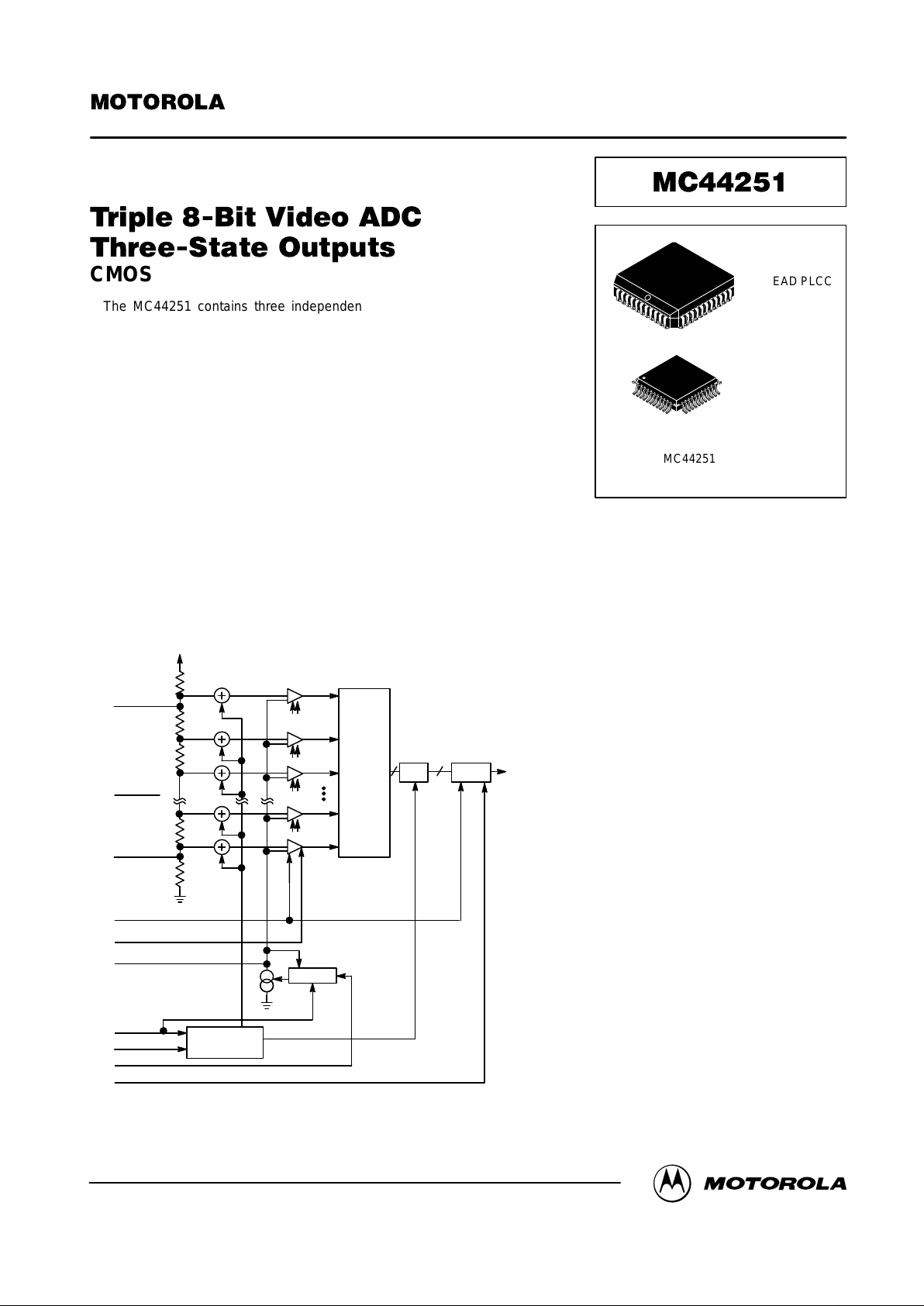
The MC44251 contains three independent parallel analog–to–digital flash
converters (ADC). Each ADC consists of 256 latching comparators and an
encoder. Video may be ac or dc coupled. With ac coupling, input clamping
provides for internal dc restoration. The MC44251 also contains a dithering
generator for video processing performance enhancements.
The MC44251 is especially suitable as a front–end converter in TV–picture
digital processing (picture–in–picture, frame storage, etc.). The high speed
conversion rate of the ADC is suitable for video bandwidth of well over 6 MHz.
• 18 MHz Maximum Sampling Rate
• Three–State Output Buffers
• Output Latching Minimizes Skew
• Input Clamps Suitable for RGB and YUV Applications
• Built–In Dither Generator with Subsequent Digital Correction
• Single 5–Volt Power Supply
• Operating Temperature Range: – 40 to + 85°C
• VTN and HZ Input Threshold Hysteresis Built–In
CLAMP
R
TOP
R
MID
R
BOT
ANALOG INPUT
HZ
MODE
VTN
I
bias
88
Σ
8
DATA
OUTPUTS
V
DD(R)
CS
DITHERING
GENERATOR
LATCH
SIMPLIFIED BLOCK DIAGRAM OF ONE OF THE ADCs
CLOCK
ENCODER
This document contains information on a new product. Specifications and information herein are subject to change without notice.
Order this document
by MC44251/D
SEMICONDUCTOR TECHNICAL DATA
FN SUFFIX
44–LEAD PLCC
CASE 777
ORDERING INFORMATION
MC44251FN PLCC
MC44251FU QFP
44
1
44
1
FU SUFFIX
44–LEAD QFP
CASE 824A
NOTE:
The FN package is not
recommended for new designs.
It is scheduled for phase out
in late 1996.
Motorola, Inc. 1996
REV 4
7/96
Page 2
MC44251 MOTOROLA
2
PIN ASSIGNMENTS
7
8
9
10
11
12
13
14
15
16
17
39
38
37
36
35
34
33
32
31
30
29
1819202122232425262728
65432
1
4443424140
B7
G0
G1
G2
G3
CS
G4
G5
G6
G7
R0
VB6B5B4VB3B2B1B0
MODE
V
V
R7
R5
CLOCK
R4
V
R3
R2
R1
I
bias
V
SS(R)
B
in
R
BOT
G
in
R
MID
R
in
R
TOP
V
DD(R)
VTN
HZ
DD(D)
SS(D)
DD(A)
R6
DD(D)
SS(D)
V
SS(A)
QFP
1
2
3
4
5
6
7
8
9
10
11
33
32
31
30
29
28
27
26
25
24
23
1213141516171819202122
4443424140393837363534
B7
G0
G1
G2
G3
CS
G4
G5
G6
G7
R0
VB6B5B4VB3B2B1B0
MODE
V
V
R7
R5
CLOCK
R4
V
R3
R2
R1
I
bias
V
SS(R)
B
in
R
BOT
G
in
R
MID
R
in
R
TOP
V
DD(R)
VTN
HZ
DD(D)
SS(D)
DD(A)
R6
DD(D)
SS(D)
V
SS(A)
PLCC
ABSOLUTE MAXIMUM RATINGS
Symbol Characteristic Value Unit
V
DD(A)
, V
DD(D)
,
V
DD(R)
DC Supply Voltage (referenced to
VSS)
– 0.5 to + 6.0 V
V
in
Input Voltage, All Pins – 0.5 to VDD + 0.5 V
I
in
DC Input Current per Pin ± 20 mA
I
out
DC Output Current per Pin ± 25 mA
T
stg
Storage Temperature Range – 65 to + 150 °C
NOTE: Maximum Ratings are those values beyond which damage to the device may occur.
Functional operation should be restricted to the Recommended Operating
Conditions.
ELECTRICAL CHARACTERISTICS (Voltages Referenced to V
SS
) (V
DD(R)
= V
DD(A)
= V
DD(D)
; R
bias
(Pin 33) = 5 kΩ to ground)
OPERATING RANGES
Symbol Characteristic Min Max Unit
V
DD(A)
, V
DD(D)
,
V
DD(R)
Power Supply Voltage 4.5 5.5 V
I
DD(A)
Analog Supply Current — 55 mA
I
DD(R)
Reference Supply Current —
28
mA
I
DD(D)
Digital Supply Current — 5 mA
T
A
Operating Ambient Temperature Range – 40 + 85 °C
A/D CONVERTER
Symbol Characteristic Min Max Unit
C
in
Input Capacitance — 60 pF
V
min
See Figure 11 0.3 x V
DD
0.36 x V
DD
V
V
max
See Figure 11 0.89 x V
DD
0.93 x V
DD
V
V
range
See Figure 11 0.57 x V
DD
0.59 x V
DD
V
Gain See Figure 11 (Note 1) 0.95 1.0 LSB
DNL Differential Nonlinearity (Note 1) — ± 1.0 LSB
INL Integral Nonlinearity (Note 1) — ± 2.0 LSB
E
gain
Gain Difference (Note 2) — ± 1.0 %
E
off
Offset Difference (Notes 1, 2) — ± 3.0 LSB
This device contains protection circuitry to
guard against damage due to high static voltages or electric fields. However, precautions
must be taken to avoid applications of any
voltage higher than maximum rated voltages to
this high–impedance circuit. For proper operation, Vin and V
out
should be constrained to the
range VSS ≤ (Vin or V
out
) ≤ VDD.
Unused inputs must always be tied to an
appropriate logic voltage level (e.g., either V
SS
or VDD). Unused outputs must be left open.
Page 3
MC44251MOTOROLA
3
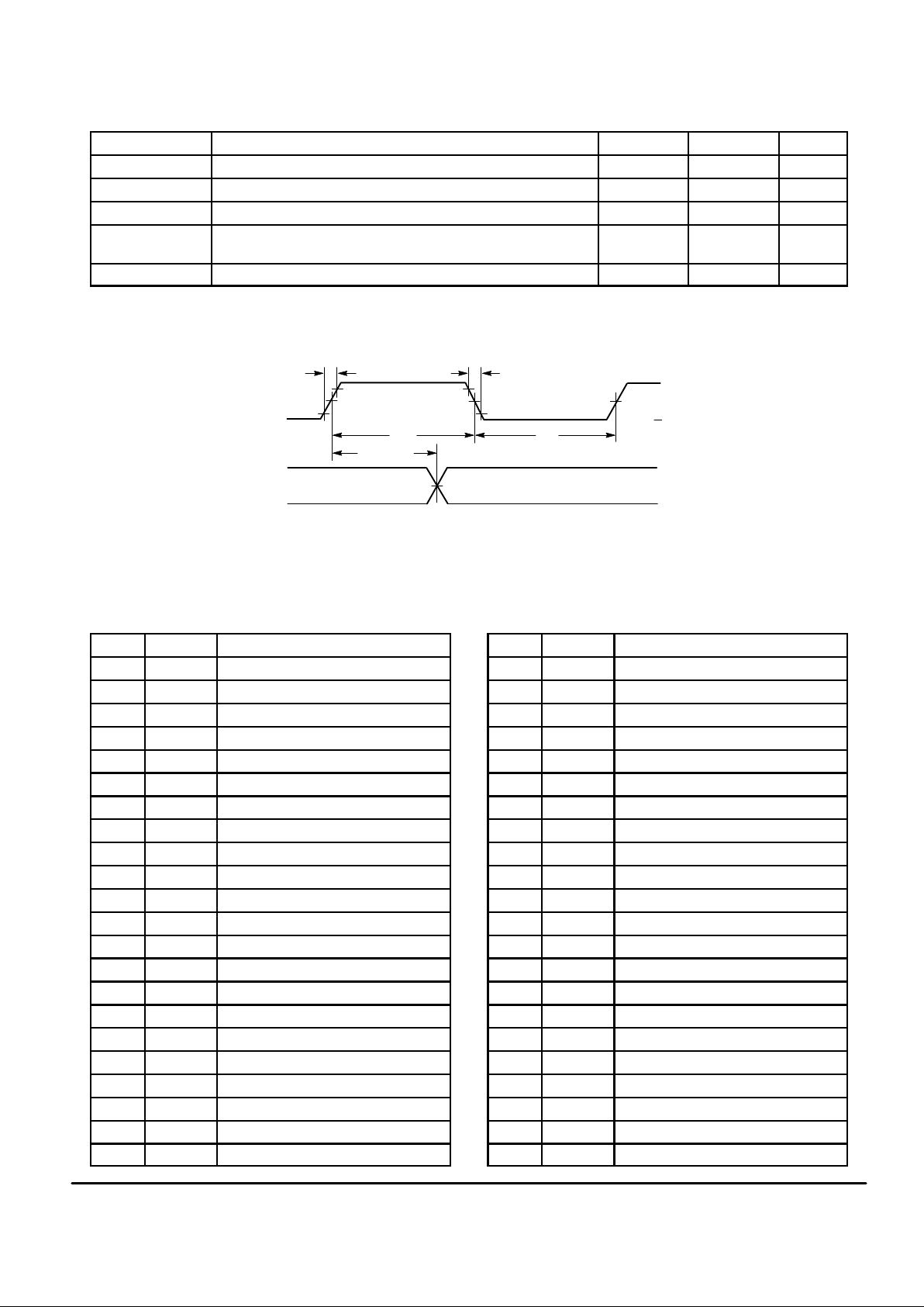
CLOCK INPUT
Symbol Characteristic Min Max Unit
V
IH
Clock Input High Level 4.2 — V
V
IL
Clock Input Low Level — 0.8 V
I
IL
Low Level Input Current — ± 2.0 µA
I
IH
High Level Input Current — ± 2.0 µA
RATE Conversion Rate — 18 ms/s
t
wL
Clock Low Duration, Figure 1 27.5 — ns
t
wH
Clock High Duration, Figure 1 27.5 — ns
t
r
Clock Rise Time (10% to 90%), Figure 1 — 15 ns
t
f
Clock Fall Time (10% to 90%), Figure 1 — 15 ns
HZ AND VTN INPUTS
Symbol Characteristic Min Max Unit
V
IH
HZ and VTN Input Turn–On Threshold Voltage 0.56 x V
DD
— V
V
IL
HZ and VTN Input Turn–Off Threshold Voltage — 0.29 x V
DD
V
V
HYS
Hysteresis Voltage 0.11 x V
DD
0.17 x V
DD
V
I
IL
Low Level Input Current — ± 2.0 µA
I
IH
High Level Input Current — ± 2.0 µA
t
H
HZ High Time, Figure 3 3 — ns
CHIP SELECT INPUT
Symbol Characteristic Min Max Unit
V
IH
Input High Level 3.5 — V
V
IL
Clamping Source Current — 1.5 V
I
IN
Input Leakage Current — ± 2.0 µA
CLAMPING NETWORK (Measured on R,G,B Inputs)
Symbol
Characteristic Min Max Unit
I
sink
Clamping Sink Current 2.0 5.0 µA
I
source
Clamping Source Current – 5.0 – 2.0 µA
D
ICL
Clamping Current Difference (Note 2) — 0.5 µA
n
V
damp
Clamping Levels (Max. Deviation Compared to Table 1) — ± 1.5 LSB
RESISTIVE REFERENCE NETWORK
Symbol Characteristic Min Max Unit
Z
TOP
R
TOP
Output Impedance 28 48 Ω
Z
BOT
R
BOT
Output Impedance 70 130 Ω
Z
MID
R
MID
Output Impedance 70 130 Ω
MODE INPUT
Symbol Characteristic Min Max Unit
V
IL
Logical “0” Level 0 0.8 V
V
IH
Logical “1” Level 4.2 V
DD(D)
V
V
IZ
Logical “Open” Level 2 2.8 V
I
IL
Input Current at “0” Level — ± 50 µA
I
IH
Input Current at “1” Level — ± 80 µA
I
IZ
Input Current at “Open” Level — ± 50 µA
Page 4
MC44251 MOTOROLA
4
DATA OUTPUTS
Symbol Characteristic Min Max Unit
t
d
Delay from Sample Clock to Valid Output, Figure 2 2.5 2.5 Cycle
I
OL
Output Sinking Current at V
out
= 0.4 V 2.0 — mA
I
OH
Output Sourcing Current at V
out
= VDD – 0.1 V – 0.4 — mA
t
QLH
, t
QHL
Propagation Delay from the Clock Rising Edge to Valid Data Output
(CL = 15 pF), Figure 1
— 40 ns
I
OTR
Maximum Three–State Leakage Current — ± 50 µA
NOTES:
1. Unit “LSB” means ideal LSB (see definitions section).
2. “Difference” means difference between any two converters in the same package.
50%
CLK
V
DD(D)
V
SS(D)
t
f
10%
90%
t
r
t
wH
t
wL
DATA
OUTPUT
50%
t
QLH
, t
QHL
Figure 1. Clock and Output Timing
PIN DESCRIPTIONS
Pin No. Name Function
1 B7 Output Blue, Bit 7 (MSB)
2 G0 Output Green, Bit 0 (LSB)
3 G1 Output Green, Bit 1
4 G2 Output Green, Bit 2
5 G3 Output Green, Bit 3
6 CS Chip Select
7 G4 Output Green, Bit 4
8 G5 Output Green, Bit 5
9 G6 Output Green, Bit 6
10 G7 Output Green, Bit 7 (MSB)
11 R0 Output Red, Bit 0 (LSB)
12 V
DD(D)VDD
, Digital
13 R1 Output Red, Bit 1
14 R2 Output Red, Bit 2
15 R3 Output Red, Bit 3
16 V
SS(D)VSS
, Digital
17 CLK Clock Input
18 R4 Output Red, Bit 4
19 R5 Output Red, Bit 5
20 R6 Output Red, Bit 6
21 R7 Output Red, Bit 7 (MSB)
22 V
SS(A)VSS
, Analog
Pin No. Name Function
23 HZ Horizontal Sync
24 VTN Vertical Sync
25 V
DD(R)VDD,
reference
26 R
TOP
Reference Tapping, Top
27 R
in
Analog Input, Red
28 R
MID
Reference Tapping, Middle
29 G
in
Analog Input, Green
30 R
BOT
Reference Tapping, Bottom
31 B
in
Analog Input, Blue
32 V
SS(R)VSS
for Reference Voltage
33 I
BIAS
To External Bias Resistor
34 V
DD(A)VDD
, Analog
35 MODE Clamp Level Select Input
36 B0 Output Blue, Bit 0 (LSB)
37 B1 Output Blue, Bit 1
38 B2 Output Blue, Bit 2
39 B3 Output Blue, Bit 3
40 V
SS(D)VSS
, Digital
41 B4 Output Blue, Bit 4
42 B5 Output Blue, Bit 5
43 B6 Output Blue, Bit 6
44 V
DD(D)VDD
, Digital
Page 5

MC44251MOTOROLA
5
RESISTIVE REFERENCE NETWORK
R
TOP
(Pin 26)
R
BOT
(Pin 30)
R
MID
(Pin 28)
Taps on the reference ladder are pinned out, providing
access to the bottom (R
BOT
), the top (R
TOP
), and the middle
scale points. These pins are intended for ac bypassing as
ladder noise may present a problem. The value of the decoupling capacitor should not exceed 47 nF. Large capacitance values can cause problems because of the amount of
energy stored. When a system containing the MC44251 is
rapidly powered down and up, the capacitor voltage may
exceed the supply voltage during the power up and cause a
latch–up condition. Failure to adequately decouple these
pins can adversely affect the conversion process.
SUPPLY PINS
V
DD(A)
(Pin 34)
V
DD(D)
(Pins 44, 12)
V
DD(R)
(Pin 25)
The three types of supply pins are analog, digital, and
reference. The dc voltage applied to all four pins must be
maintained such that
V
DD(A)
= V
DD(D)
= V
DD(R)
.
Each pin must be carefully decoupled to ground as close
to the package as possible, and particular care should be
taken with V
DD(R)
as any noise present on this pin will
appear in the output data as an equivalent input noise. This
noise will be present on the Rin, Gin, and Bin input pins in a
ratio of 1:1 to the input noise (worst case condition). Noise
reduction can be improved by incorporating choke coil inductors in series with the power supply rails.
ANALOG INPUTS
Rin (Pin 27)
Gin (Pin 29)
Bin (Pin 31)
The analog signals to be converted are input at these pins.
An on–chip clamp circuit for dc restoration is available when
using ac coupling. The clamp circuit operation is activated by
the presence of the signal at the HZ input. This signal is
derived from the composite sync information and must be
coincident with the horizontal sync of the composite video
waveform for proper operation. Yin, Uin, and Vin may be used
instead of the RGB signals. In this case the conversion will
be a YUV analog–to–digital conversion.
I
bias
(Pin 33)
The comparator bias current is set by connecting an exter-
nal resistor between I
bias
and ground. The conversion rate is
guaranteed for a resistor value of 5.1 kΩ ± 5% and will
decrease logarithmically with increased resistance. The
resistor must be placed adjacent to the I
bias
pin. No decoup-
ling capacitor is allowed on this pin.
DIGITAL OUTPUTS
R0 – R7 (Pins 11, 13 – 15, 18 – 21)
G0 – G7 (Pins 2 – 5, 7 – 10)
B0 – B7 (Pins 36 – 39, 41 – 43, 1)
These pins are the parallel output for the digital value for
the RGB signals. R0 through R7 are the digital equivalent of
the analog RED input, G0 through G7 are equivalent to the
GREEN input, and B0 through B7 are equivalent to the BLUE
input. If YUV analog signals have been input instead of the
RGB signals; the digital outputs will be Y0 through Y7, U0
through U7, and V0 through V7.
DIGITAL INPUTS
Clock (Pin 17)
The analog input voltages to be converted are sensed at
the falling edge of the clock signal and the corresponding
data is present on the digital outputs at the clock signal rising
edge, 2.5 cycles later (see Figure 2).
HZ (Pin 23)
This is the horizontal synchronization input, and is used to
increment the dither generator. The clamp network is also
controlled by HZ to ensure proper dc restoration for Rin, Gin,
and Bin before conversion. Schmitt trigger input is included to
improve noise immunity.
VTN (Pin 24)
The vertical synchronization input, VTN, resets the dither
generator after every second vertical sync pulse (after each
frame). Schmitt trigger input is included to improve noise
immunity.
MODE (Pin 35)
This pin is used to select the proper clamp levels (see
Table 1).
CHIP SELECT (Pin 6)
Chip select is an active low input used to enable the ADC
for data transfers. When the CS
is at a high level, the digital
output is forced to a high impedance state.
Page 6
MC44251 MOTOROLA
6
t
d
CLK
IN
OUT
Figure 2. Conversion Timing Functional Characteristics
CIRCUIT OPERA TION
GENERAL
The MC44251 contains three independent parallel analog–to–digital converters (ADC). Each ADC consists of 256
latching comparators and an encoder. The MC44251 may be
used to convert RGB or YUV video information from an analog to a digital format, or as a triple ADC for non–video information. For video processing performance enhancement,
each ADC has a dither generator with subsequent digital
correction designed into it. The dithering generator reduces
display degradation from granulation of the luminance
information caused by quantization errors of the digitizing
process. Each ADC is driven from a common clock and
receives common sync information from the HZ and VTN
pins. In addition, the VTN pin controls the dithering function
and disables the dithering generator when VTN is pulled low.
The sampling of the analog input signals occurs at the falling
edge of the clock signal, whereas the digital outputs change
state at the rising clock edge. The bias current of the
comparators is set by an external resistor. Input clamps allow
for ac coupling of the input signals.
CLAMP NETWORK
The MC44251 can be operated either dc coupled or ac
coupled. When dc coupled, the MC44251 will track the average dc level of the input waveform. For ac coupling, an
on–chip dc restoration circuit samples and adjusts the average dc level of the input signal. The MC44251 has three
selectable clamping levels for ac coupling. The clamp levels
are selected by the MODE pin according to Table 1. In the
RGB mode, the clamping levels are set to 16/256, corresponding to 6.3% of full range. In the YUV mode, the UV
clamping levels are set to 128/256 (50%) and the Y input to
either 16/256 or 64/256 (25%).
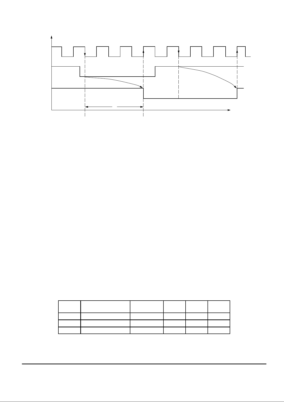
When input HZ (horizontal) is high, as illustrated in Figure 3a, the voltage difference between the analog input voltage and the clamp reference voltage is integrated within
each clamp network. At the falling edge of HZ, a latching
comparator senses the sign of the integrator output voltage.
Depending on this result, either a sinking or a sourcing current is applied to the analog input pin as long as input HZ remains low.
For video applications, the timing of HZ is critical to the
proper operation of the ADC. The frequency of HZ should be
locked to the line frequency of the video input. The pulse
width and timing of HZ with respect to the video signal is
shown in Figure 4. The top curve represents the horizontal
synchronizing and blanking interval for a video signal. The
pulse width of HZ (t
H
) should be less than the width of the
back porch (tBP) and coincident with it. In all cases, HZ must
return low before the end of the back porch (tBP).
Table 1. Clamping Levels
MODE
(Pin 35)
Application Clamp Levels G
in
R
in
B
in
L RGB 16/256 16/256 16/256
H YUV Mode Without Sync Format 16/256 128/256 128/256
Open YUV Mode With Sync 64/256 128/256 128/256
Page 7

MC44251MOTOROLA
7
Figure 3a. Operation
Figure 3b. Power Up
∆
V =
I t
L
1
C
HZ
I
C
MC44251
∆
V
t
L
HZ
I
V
clamp
I
sink
I
source
t
L
V0 – V
clamp
=I t
L
N
C
V
clamp
V
in
V
0
HZ
N PERIODS
I = I
sink
IF V0 > V
clamp
I = I
source
IF V0 < V
clamp
CLAMP
LEVEL
Figure 3. Clamp Network Timing Diagrams
Page 8

MC44251 MOTOROLA
8
VIDEO
HZ
t
H
t
BP
Figure 4. Horizontal Timing
DITHERING
Dithering can be used to reduce the errors that are the
result of the digitizing process used to convert video information between analog and digital forms. This method can
also be applied to non–video signals. When converting analog signals to a digital format, errors can be introduced
because of the limited number of discrete levels that the digital system imposes. For example, an 8–bit digital word can
describe exactly 256 discrete analog levels. In some cases,
this may not be sufficient for the application involved.
One solution is to increase the number of bits that describe
the analog signal. The disadvantages of this approach are
the increase in cost of the converter and the loss in speed
associated with the increased number of bits. The addition of
analog filters at the point where the digital information is converted back to analog is also possible, but this also has its
limitations.
When a ramp voltage is generated from a digital source or
an analog ramp is converted to a digital form and back to
analog, the limited number of vertical samples causes the
ramp to take the form of a “stair case” (see Figure 5). The
severity of this distortion depends on the number of digital
bits that generated the ramp. The “stair case” effect is less
pronounced when the number of bits producing the ramp is
increased.
When processing video information using a YUV form and
a luminance ramp is displayed, granulation errors may become noticeable. This condition can also occur when one of
the RGB signals is ramped and the other two are held
constant. When processing video information using 24 bits or
less, this “granulation” can be observed. Since the video is
processed as three 8–bit signals, the maximum number of
different luminance levels is reduced to 256. In cases where
only a 7–bit luminance signal is used, the maximum number
of luminance levels is reduced to 128. The uniform luminance ramp is observed on the display as vertical bars rather
than a uniform luminance change.
The dithering technique consists of adding a small offset to
the input signal. This offset (when it is equal to an integer
number of LSB) is then subtracted from the digital output
data. This offset is varied “line–to–line” by one half LSB
steps. It allows each point of the waveform to be interpolated
to higher precision by averaging the differential linearity
errors on the screen.
The addition of the small offset forces the comparators to
sample at a slightly different point on the input waveform (see
Figure 6). When translated to the display , the ef fect is to shift
this value slightly to the left. Overall accuracy of the display is
maintained by subtracting this value from the output when
the shift is equal to an integer number of LSB. For a uniform
and continuous video waveform, the result of incrementing
and decrementing the dither voltage is to effectively double
the luminance levels from 256 to 512. The effect is to broaden the luminance range. This results in a more pleasing display with less visible quantization.
The dithering pattern is generated by means of a binary
counter, which is incremented for every line by input HZ, and
reset by every second vertical input VTN; thus, the dithering
pattern is synchronized to the deflection of the screen. The
effect of the dithering pattern is given in Figure 7. Subsequent subtraction of the introduced dithering signal at the
output of each ADC is performed by a binary adder. The
dither counter, and hence the dithering function, may be
stopped by holding VTN low. Depending on the state of the
dither counter, the output code range can be either from $00
to $FE or from $01 to $FF.
Depending on the state of the dither counter, the output
code range can be either from S00 to SFE or from S01 to
SFF.
EXPECTED
ACTUAL
Figure 5. Distortion Produced by Digitizing
Page 9

MC44251MOTOROLA
9
ANALOG SIGNAL + DITHER
ANALOG SIGNAL
COMPARATOR LEVEL
∆
t
∆
V
Figure 6. Amplitude Dithering
Figure 7. Effect of Dithering Pattern
HZ
DITHER
0.5 LSB
0.5 LSB
0.5 LSB
0
0.75 LSB
– 0.75 LSB
Figure 8. Dithering Sequence
Page 10

MC44251 MOTOROLA
10
RESTRICTIONS ON V
DD(R)
The normal operating condition for the MC44251 is defined
as V
DD(R)
= V
DD(A)
= V
DD(D)
and the safe operating
range of V
DD(R)
is defined as 0 ≤ V
DD(R
)
≤VDD. In cases
where V
DD(R)
is operated at values other than VDD, it should
be noted that the accuracy of the conversion process is reduced. In all cases V
DD(R)
should not be allowed to exceed
VDD.
The step size is defined as SS(n) and the ideal step size is
defined as SSI. We may define an error component, ∂, as the
difference between the actual step size and the ideal step
size so that
∂ = |SSI – SS(n)|.
We may also define a worst case value for ∂ as
∂ ≤ ∂w
where ∂w is the greatest value of ∂. The origin of this error is
the offset mismatch from one comparator to another and is
nearly independent of V
DD(R)
and VDD.
Since ∂ is nearly independent of V
DD(R)
, its value will re-
main constant for all values of V
DD(R)
.
The step size error, SSE, is defined as
SSE(n) = (SSI – SS(n))/SSI = ∂(n)/SSI.
Furthermore, the ideal step size SSI is defined as
SSI = V
DD(R)
× 0.6/255.
Since ∂ is a constant and SSI is proportional to V
DD(R)
, the
step size error, SSE, will increase as V
DD(R)
is decreased.
Further study will show that the differential nonlinearity, DNL,
will also increase as V
DD(R)
is reduced. To minimize these
errors it is desirable to keep V
DD(R)
as high as possible.
Since the maximum value for V
DD(R)
is VDD,
V
DD(R)
= V
DD(D)
= V
DD(A)
is the value that produces the greatest conversion accuracy.
INPUT VOLTAGE RANGE
In applications where the input signals are dc coupled to
the MC44251, the following restrictions apply:
If Vin ≤ V
min
, then the output code = $00 or $01 (depending
on the dither generator).
If Vin ≥ V
max
, then the output code = $FE or $FF (depend-
ing on the dither generator).
If V
min
≤ Vin ≤ V
max
, then the output code reflects the cor-
rect value of the input voltage.
If the input is video based and ac coupled, then the input
voltage range for Vin without saturation is
0 ≤ V
in
≤ V
range
.
For Vin this reflects a maximum video input level before
saturation of about 3 V for VDD = 5 V.
DEFINITIONS
n+4
VM (n+3)
n+3
n+2
n+1
n
VT (n)
VT (n+1) VT (n+2)
VT (n+3)
V
in
OUTPUT
CODE
Figure 9.
• Transition Voltage: Voltage at which transition from step
n to step n+1 occurs = VT(n).
• Step Size: Difference between two consecutive transition
voltages.
SS(n)+VT(n)*VT(n*1)
• Mid–Point Voltage:
VM(n)
+
VT(n))VT(n*1)
2
VM(max code)
+
V
DD(R)
)
VT(max code*1)
2
Page 11

MC44251MOTOROLA
11
•
Step Size Ideal:
V
range
255
+
SSI
• Differential Nonlinearity (D
NL
):
DNL(n)
+
VM(n)1)–VM(n)
SSI
–1 in LSB
• Integral Nonlinearity (I
NL
) and Offset:
Note: INL (min code) and INL (max code) is not defined.
• Gain: Gain = a in the formula Y = a • code + b
or the slope in the curve mid–points = f(code)
• V
offset
: V
offset
= b – V
min
n+4n+3n+2n+1n
Y = a • code + b
MID–POINTS
OUTPUT
CODE
LEAST SQUARE
FIT LINE
V
offset
INL (n+5)
n+6n+5
MID–POINT
VOLTAGE
V
min
Figure 10. Integral Nonlinearity and Offset
DC INPUT VOLTAGE
OUTPUT CODE
MAX CODE*
MIN CODE*
1/GAIN = SLOPE
V
min
V
max
V
range
*See dither generator .
LSB ideal = V
range
/255
(Min code = 0 or 1; see dither generator)
Figure 11.
INL(n)
+
VM(n)*a
·
n*b
SSI
in LSB
Page 12

MC44251 MOTOROLA
12
APPLICATION INFORMATION
PCB DESIGN
To maximize the performance of the MC44251, noise
should be kept to a minimum. Good printed circuit board design will enhance the operation of the MC44251. Separate
analog and digital grounds will reduce noise and conversion
errors. In addition, separate filters on analog VCC and digital
VDD will also help to minimize noise and conversion errors.
Sufficient decoupling and short leads will also improve performance.
When designing mixed analog/digital printed circuit
boards, separate ground planes for digital ground and analog
ground should be employed. Large switching currents generated by digital circuits will be amplified by analog circuitry
and can quickly make a circuit unusable. Care should be taken to ensure analog ground does not inadvertently become
part of the digital ground. The analog and digital grounds
should be connected together at only one point. This is usually at or near where power enters the printed circuit board.
Additionally, when interconnecting several printed circuit
boards together, care must be taken to ensure that cabling
does not interconnect digital and analog grounds together to
produce a path for digital switching currents through analog
ground.
When using any device with the performance and speed of
the MC44251, ground planes are essential. Loosely interconnected traces and/or random areas of ground strewn
around the printed circuit board are inadequate for high performance circuitry. While distribution of VDD and VCC can be
done by bussing, to do so with the ground system is disastrous.
An inch long conductor is an 18 nH inductor. The cross
sectional area of the conductor affects the exact value of the
inductance, but for most PCB traces this is approximately
correct. If the ground system is composed of traces or
clumps of ground loosely interconnected, it will be inductive.
The amount of inductance will be proportional to the length of
the conductors making up the ground. This inductance cannot be decoupled away. It must be designed out.
A CMOS device exhibits a characteristic input capacitance
of about 10 pF. If this gate is driven by a digital signal that
switches 2.5 V in a period of 5 ns, the equation for the average current flowing during the switching time will be:
IAV = Cdv/dt.
A voltage change of 2.5 V in 5 ns requires an average current of 5 mA. If we assume a linear ramp starting from zero,
the total change in current will be 10 mA. The change in current per nanosecond per gate can be found by dividing the
change in current by the time
10 mA/5 ns = 2 mA/ns.
For a device with 16 outputs driving one gate for each output,
di/dt = 16 × 2 mA/ns = 32 mA/ns.
If the above 1–inch wire is in this current path, then the
voltage dropped across it can be found from the formula
V = Ldi/dt = 18 nH × 32 mA/ns = 0.576 V.
If the inductor is in the ground system, it is in the signal
path. The voltage generated by the switching currents
through this inductor will be added to the signal. At best it will
be superimposed on the analog signal as unwanted noise. At
worst, it can render the entire circuit unusable. Even the digital signal path is not immune to this type of signal. It can false
trigger clock circuits causing timing errors, confuse comparator type circuits, and cause digital signals to be misinterpreted as wrong values.
When laying out the PCB, use electrolytic capacitors of
sufficient size at the power input to the printed circuit board.
Adding low ESR decoupling capacitors of about 0.1 µF
capacitance across VCC and/or VDD at each device will help
reduce noise in general and ESD susceptibility. Implementation of a good ground plane ground system can all but eliminate the type of noise described above.
To summarize, use sufficient electrolytic capacitor filtering,
make separate ground planes for analog ground and digital
ground, tie these grounds together at one and only one point,
keep the ground planes as continuous and unbroken as possible, use low ESR capacitors of about 0.1 µF capacitance
on VCC and VDD at each device, and keep all leads as short
as possible.
EMI SUPPRESSION
When using ICs in or near television receiver circuits, EMI
(electromagnetic interference) and subsequent unwanted
display artifacts and distortion are probable unless adequate
EMI suppression is implemented. A common misconception
is that some offending digital device is the culprit. This is erroneous in that an IC itself has insufficient surface area to
produce sufficient radiation. The device, while it is the generator of interfering signals, must be coupled to an antenna before EMI is radiated. The source for the EMI is not the IC
which generates the offending signals but rather the circuitry
which is attached to the IC.
Potential EMI signals are generated by
all
digital devices.
Whether they become a nuisance is dependent upon their
frequency and whether they have a sufficient antenna. The
frequency and number of these signals is affected by both
circuit design within the IC and the manufacturing process.
Device speed is also a major contributor of potential EMI. Because the design is determined by the anticipated application, the manufacturing process is fixed and the drive for
speed ever increasing, the only effective point to implement
EMI suppression is in the PC board design. The PC board
usually is the antenna which radiates the EMI. The most efficient method of minimizing EMI radiation is to minimize the
efficiency of this antenna.
The most common cause of inadequate EMI suppression
lies with the ground system of the suspected digital devices.
As pointed out previously, di/dt transitions can be significant
in digital circuits. If the di/dt transitions appear in the ground
system and the ground system is inductive, the harmonics
present in these transitions are a source of potential EMI signals. The unfortunate result of putting digital devices on a
reactive ground system is guaranteed EMI problems.
The area which should be addressed first as a potential
EMI source is the ground. Without an adequate ground system, EMI cannot be effectively reduced by decoupling. If at
all possible, the ground should be a complete unbroken
plane. Figure 12 shows two examples of relieving ground
around device pins. When relieving vias and plated through
holes, large areas of ground loss should be avoided. When
Page 13

MC44251MOTOROLA
13
the relief pattern is equal to half the distance between pins,
over etching and process errors may remove ground between pins. If sufficient ground around enough pins is removed, the ground system can become isolated or nearly
isolated “patches” which will appear inductive. If ground,
such as the vicinity of an IC, must be removed, replace with
a cross hatch of ground lines with the mesh as small as possible.
If a single unbroken plane can be devoted to the ground
system, EMI can usually be sufficiently suppressed by using
ferrite beads on suspect EMI paths and decoupling with adequate values of capacitors. The value of the decoupling
capacitor depends on the frequency and amplitude of the
offending signals. Ferrite beads are available in a wide variety of shape, size and material to fit virtually any application.
Choose a ferrite bead for desired impedance at the desired frequency and construct a low pass filter using one or
more appropriate capacitors in a “L”, “T”, or “PI” arrangement. Use only capacitors of low inductive and resistive
properties such as ceramic or mica. Install filters in series
with each IC pin suspected of contributing offending EMI
signals and as close to the pin as possible. Analysis using a
spectrum analyzer can help determine which pins are
suspect.
Where PC board costs constrain the number of layers
available, and if the EMI frequencies are far removed from
the frequencies of operation, ferrite beads and decoupling
capacitors may still be effective in reducing EMI emissions.
Where only two (or in some cases, only one) layer is used,
the ground system is always reactive and poses an EMI
problem. If the offending EMI and normal operating frequency differ sufficiently, filtering can still work.
An “island” is constructed in the ground system for the digital device using ferrite beads and decoupling capacitors as
shown by the example in Figure 13. The ground must be cut
so that the digital ground for the device is isolated from the
rest of the ground system. Next choose a ferrite bead of the
appropriate value. Install this bead between the isolated
ground and the ground system. Install low pass filters in all
suspect lines with the capacitor closest to the device pin connected to the isolated ground in all signal lines where EMI is
suspect. Also cut the power to the device and insert a ferrite
bead as shown in Figure 13. Finally , decouple the device between the power pin(s) and isolated ground pin(s) using a
low inductive/resistive capacitor of adequate value.
The methods described above will work acceptably when
the EMI frequency and the frequency of operation of the
device generating the EMI differ greatly. Where the EMI is
disturbing the high VHF or UHF channels and the device
generating the EMI is operating within the NTSC/PAL bandwidth, the energy contained in the harmonics generating the
EMI is situated well above the operating frequency and
suppressing this type of EMI poses no great problem. However, if the EMI is present on low VHF channels and/or the
operation of the device is outside the NTSC/PAL bandwidth,
such as a 2X pixel clock or 4xfsc oscillator, compromise between video quality and suppression complexity is usually required to obtain an acceptable solution. For those cases
where the operating frequency of the device is very near the
frequency of the EMI disturbance, careful attention to PCB
layout, multiple layer PCB and even shielding may be necessary to obtain an acceptable design.
APPLICATION CIRCUIT
Figure 14 shows a typical application circuit. This circuit
will produce analog–to–digital conversion of either RGB information or YUV information by setting SW1. In the YUV
mode, SW1 is set either to position ‘1’ or to the open position
depending on the desired clamp level (see Table 1). The
RGB inputs then become YUV inputs and correspondingly,
the RGB outputs are YUV. For RGB operation, SW1 is set to
the ‘0’ position.
Page 14

MC44251 MOTOROLA
14
BETTERWRONG
Figure 12.
POWER
INPUT OR
OUTPUT
SIGNAL
GROUND
LOW PASS
FILTER
0.1 µF DECOUPLING
FERRITE BEAD
FERRITE BEAD
CUT
CUT
FERRITE BEAD
Figure 13.
Page 15

MC44251MOTOROLA
15
+ 5 V
V
DD(A)
MODE
B0
B1
B2
B3
V
SS(D)
B4
B5
B6
V
DD(D)
V
SS(A)
R7
R6
R5
R4
CLK
V
SS(D)
R3
R2
R1
V
DD(D)
I
bias
V
SS(R)
B
in
R
BOT
G
in
R
MID
R
in
R
TOP
V
DD(R)
VTN
HZ
B7G0G1G2G3
G4G5G6G7R0
D
AAAA
47 nF47 nF47 nF
AD
100 nF 4.7 nF 4.7 nF 4.7 nF
100 nF
SW1
1
0
100 nF
10 TO 100
10 TO 100
+ 5 V
R
in
GinB
in
VTN
HZ
CLK
100 nF
R [7..0]
B [7..0]
G [7..0]
5.1 k
A
D
MC44251
CS
D
CS
10
µ
F
47
µ
F
µ
H
µ
H
Figure 14. Application Circuit
Page 16

MC44251 MOTOROLA
16
P ACKAGE DIMENSIONS
FN SUFFIX
PLCC PACKAGE (PLASTIC LEAD CHIP CARRIER)
CASE 777–02
NOTES:
1. DATUMS –L–, –M–, AND –N– ARE DETERMINED
WHERE TOP OF LEAD SHOULDER EXITS
PLASTIC BODY AT MOLD PARTING LINE.
2. DIMENSION G1, TRUE POSITION TO BE
MEASURED AT DATUM –T–, SEATING PLANE.
3. DIMENSIONS R AND U DO NOT INCLUDE MOLD
FLASH. ALLOWABLE MOLD FLASH IS 0.010
(0.25) PER SIDE.
4. DIMENSIONING AND TOLERANCING PER ANSI
Y14.5M, 1982.
5. CONTROLLING DIMENSION: INCH.
6. THE PACKAGE TOP MAY BE SMALLER THAN
THE PACKAGE BOTTOM BY UP TO 0.012
(0.300). DIMENSIONS R AND U ARE
DETERMINED AT THE OUTERMOST
EXTREMES OF THE PLASTIC BODY
EXCLUSIVE OF MOLD FLASH, TIE BAR BURRS,
GATE BURRS AND INTERLEAD FLASH, BUT
INCLUDING ANY MISMATCH BETWEEN THE
TOP AND BOTTOM OF THE PLASTIC BODY.
7. DIMENSION H DOES NOT INCLUDE DAMBAR
PROTRUSION OR INTRUSION. THE DAMBAR
PROTRUSION(S) SHALL NOT CAUSE THE H
DIMENSION TO BE GREATER THAN 0.037
(0.940). THE DAMBAR INTRUSION(S) SHALL
NOT CAUSE THE H DIMENSION TO BE
SMALLER THAN 0.025 (0.635).
–N–
–L–
–M–
D
Y
D
K
V
W
144
BRK
B
Z
U
X
VIEW D–D
S
L–M
M
0.007(0.180) N
S
T
S
L–M
M
0.007(0.180) N
S
T
G1
S
L–M
S
0.010 (0.25) N
S
T
K1
F
H
S
L–M
M
0.007(0.180) N
S
T
Z
G
G1
R
A
E
J
VIEW S
C
S
L–M
M
0.007(0.180) N
S
T
S
L–M
M
0.007(0.180) N
S
T
0.004 (0.10)
–T–
SEATING
PLANE
VIEW S
DIM MIN MAX MIN MAX
MILLIMETERSINCHES
A 0.685 0.695 17.40 17.65
B 0.685 0.695 17.40 17.65
C 0.165 0.180 4.20 4.57
E 0.090 0.110 2.29 2.79
F 0.013 0.019 0.33 0.48
G 0.050 BSC 1.27 BSC
H 0.026 0.032 0.66 0.81
J 0.020 ––– 0.51 –––
K 0.025 ––– 0.64 –––
R 0.650 0.656 16.51 16.66
U 0.650 0.656 16.51 16.66
V 0.042 0.048 1.07 1.21
W 0.042 0.048 1.07 1.21
X 0.042 0.056 1.07 1.42
Y ––– 0.020 ––– 0.50
Z 2 10 2 10
G1 0.610 0.630 15.50 16.00
K1 0.040 ––– 1.02 –––
S
L–M
S
0.010 (0.25) N
S
T
S
L–M
M
0.007(0.180) N
S
T
____
Page 17

MC44251MOTOROLA
17
FU SUFFIX
QFP (QUAD FLAT PACKAGE)
CASE 824A–01
NOTES:
1. DIMENSIONING AND TOLERANCING PER ANSI
Y14.5M, 1982.
2. CONTROLLING DIMENSION: MILLIMETER.
3. DATUM PLANE –H– IS LOCATED AT BOTTOM OF
LEAD AND IS COINCIDENT WITH THE LEAD WHERE
THE LEAD EXITS THE PLASTIC BODY AT THE
BOTTOM OF THE PARTING LINE.
4. DATUMS –A–, –B– AND –D– TO BE DETERMINED AT
DATUM PLANE –H–.
5. DIMENSIONS S AND V TO BE DETERMINED AT
SEATING PLANE –C–.
6. DIMENSIONS A AND B DO NOT INCLUDE MOLD
PROTRUSION. ALLOWABLE PROTRUSION IS 0.25
(0.010) PER SIDE. DIMENSIONS A AND B DO
INCLUDE MOLD MISMATCH AND ARE DETERMINED
AT DATUM PLANE –H–.
7. DIMENSION D DOES NOT INCLUDE DAMBAR
PROTRUSION. ALLOWABLE DAMBAR PROTRUSION
SHALL BE 0.08 (0.003) TOTAL IN EXCESS OF THE D
DIMENSION AT MAXIMUM MA TERIAL CONDITION.
DAMBAR CANNOT BE LOCATED ON THE LOWER
RADIUS OR THE FOOT.
L
33
34
23
22
44
111
12
DETAIL A
–D–
–A–
A
S
A–B
M
0.20 (0.008) D
S
C
S
A–B
M
0.20 (0.008) D
S
H
0.05 (0.002)
A–B
S
B
S
A–B
M
0.20 (0.008) D
S
C
S
A–B
M
0.20 (0.008) D
S
H
0.05 (0.002)
A–B
V
L
–B–
–C–
SEATING
PLANE
M
M
E
H
G
C
–H–
DATUM
PLANE
DETAIL C
0.01 (0.004)
M
–H–
DATUM
PLANE
T
R
K
Q
W
X
DETAIL C
DIM MIN MAX MIN MAX
INCHESMILLIMETERS
A 9.90 10.10 0.390 0.398
B 9.90 10.10 0.390 0.398
C 2.10 2.45 0.083 0.096
D 0.30 0.45 0.012 0.018
E 2.00 2.10 0.079 0.083
F 0.30 0.40 0.012 0.016
G 0.80 BSC 0.031 BSC
H ––– 0.25 ––– 0.010
J 0.013 0.23 0.005 0.009
K 0.65 0.95 0.026 0.037
L 8.00 REF 0.315 REF
M 5 10 5 10
N 0.13 0.17 0.005 0.007
Q 0 7 0 7
R 0.13 0.30 0.005 0.012
S 12.95 13.45 0.510 0.530
T 0.13 ––– 0.005 –––
U 0 ––– 0 –––
V 12.95 13.45 0.510 0.530
W 0.40 ––– 0.016 –––
X 1.6 REF 0.063 REF
DETAIL A
B
B
–A–, –B–, –D–
S
A–B
M
0.20 (0.008) D
S
C
F
N
SECTION B–B
J
D
BASE METAL
____
____
__
Page 18

MC44251 MOTOROLA
18
Motorola reserves the right to make changes without further notice to any products herein. Motorola makes no warranty , representation or guarantee regarding
the suitability of its products for any particular purpose, nor does Motorola assume any liability arising out of the application or use of any product or circuit, and
specifically disclaims any and all liability, including without limitation consequential or incidental damages. “T ypical” parameters which may be provided in Motorola
data sheets and/or specifications can and do vary in different applications and actual performance may vary over time. All operating parameters, including “Typicals”
must be validated for each customer application by customer’s technical experts. Motorola does not convey any license under its patent rights nor the rights of
others. Motorola products are not designed, intended, or authorized for use as components in systems intended for surgical implant into the body, or other
applications intended to support or sustain life, or for any other application in which the failure of the Motorola product could create a situation where personal injury
or death may occur. Should Buyer purchase or use Motorola products for any such unintended or unauthorized application, Buyer shall indemnify and hold Motorola
and its officers, employees, subsidiaries, affiliates, and distributors harmless against all claims, costs, damages, and expenses, and reasonable attorney fees
arising out of, directly or indirectly, any claim of personal injury or death associated with such unintended or unauthorized use, even if such claim alleges that
Motorola was negligent regarding the design or manufacture of the part. Motorola and are registered trademarks of Motorola, Inc. Motorola, Inc. is an Equal
Opportunity/Affirmative Action Employer.
How to reach us:
USA/EUROPE /Locations Not Listed: Motorola Literature Distribution; JAPAN: Nippon Motorola Ltd.; T atsumi–SPD–JLDC, 6F Seibu–Butsuryu–Center,
P.O. Box 20912; Phoenix, Arizona 85036. 1–800–441–2447 or 602–303–5454 3–14–2 Tatsumi Koto–Ku, Tokyo 135, Japan. 03–81–3521–8315
MFAX: RMF AX0@email.sps.mot.com – TOUCHT ONE 602–244–6609 ASIA /PACIFIC: Motorola Semiconductors H.K. Ltd.; 8B Tai Ping Industrial Park,
INTERNET: http://Design–NET.com 51 Ting Ko k Road, Tai Po, N.T., Hong Kong. 852–26629298
MC44251/D
*MC44251/D*
◊
 Loading...