

Page 1
Order this document by MC44145/D
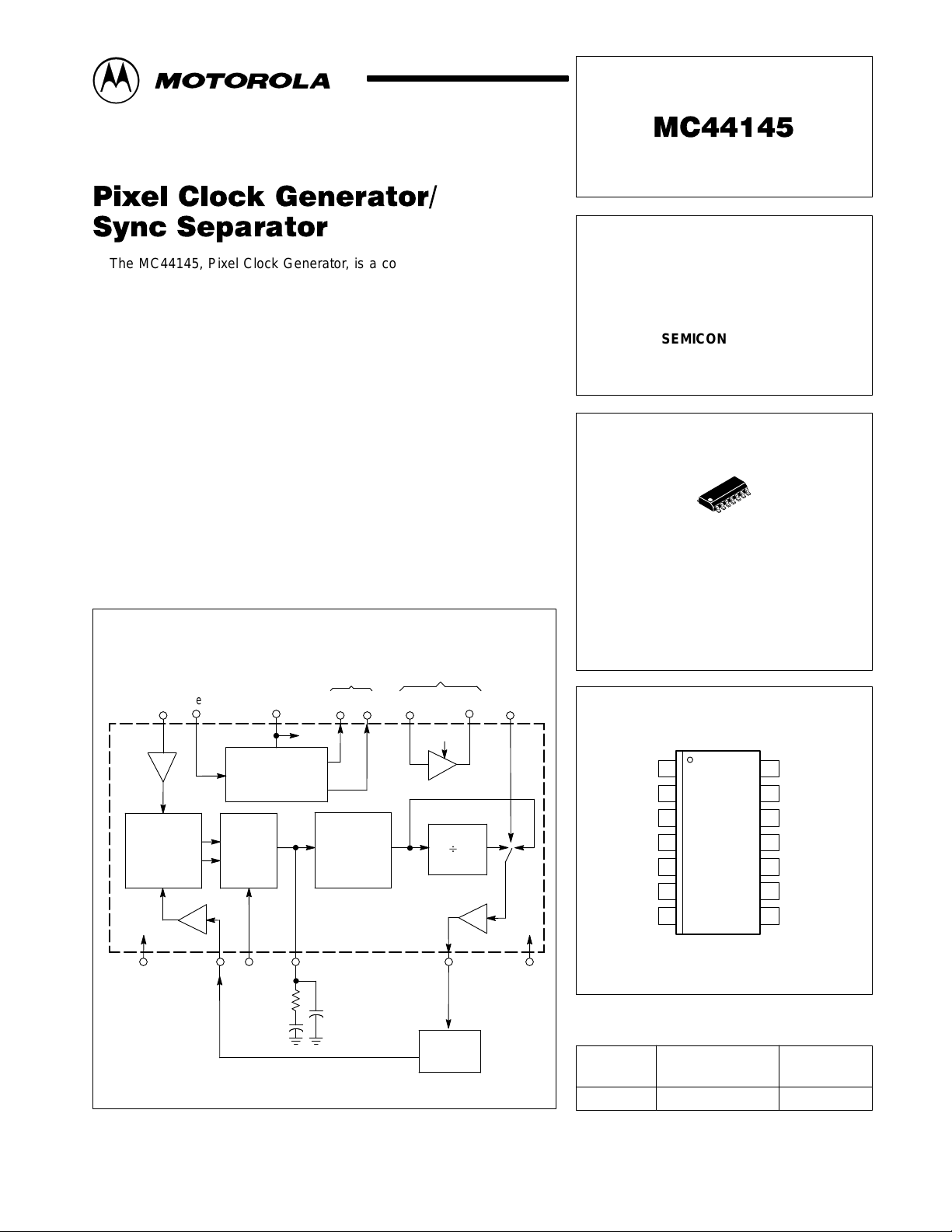
The MC44145, Pixel Clock Generator, is a component of the MC44000
family.
The MC44145 contains a sync separator with composite sync and vertical
outputs, and clock generation circuitry for the digitization of any video signal
along with the necessary circuitry for clock generation, such as a phase
comparator and a divide–by–2 to provide a 50% duty cycle.
The MC44145 is available in a SO–14 package and is fabricated in the
Motorola high density, high speed, low voltage, process called MOSAIC 1.5.
MOSAIC is a trademark of Motorola, Inc.
Representative Block Diagram
V
CC
Video InF
ref
12 11953 4 10 8
Sync Sep
Sync Out Sync Amp
A
InCB
A
Out
Div 2
EN
PIXEL CLOCK GENERATOR/
SYNC SEPARATOR
SEMICONDUCTOR
TECHNICAL DATA
14
1
D SUFFIX
PLASTIC PACKAGE
CASE 751A
(SO–14)
PIN CONNECTIONS
Sync
Separator
Phase and
Frequency
Comparator
613114 7 2
V
CC
Up
Charge
Pump
Dn
NBACK NPD
Gain
This device contains 214 active transistors.
V
C
VCO
MC44145
PLL Loop
Filter
R
C
C2
B
2
Clock Out Gnd
External
Divider
2F
F
O
O
MOTOROLA ANALOG IC DEVICE DATA
NPD Gain
Gnd
Sync B
Sync Amp In
Sync C
V
CC
Clock Out
1
2
3
4
5
6
7
(Top View)
PLL Loop Filter
14
NBACK
13
Video In
12
V
11
CC2
Sync Amp Out
10
F
9
ref
Div 2 EN
8
ORDERING INFORMATION
Operating
Device
MC44145D TA = 0° to +70°C SO–14
Motorola, Inc. 1996 Rev 0
Temperature Range
Package
1
Page 2
MC44145
MAXIMUM RATINGS
Rating Symbol Value Unit
Supply Voltage V
Storage Temperature Range T
Operating Junction Temperature T
NOTE: ESD data available upon request.
V
CC
CC2
stg
J
RECOMMENDED OPERATING CONDITIONS
Characteristic Symbol Pin Min Typ Max Unit
Supply Voltage V
Video Input Amplitude (Note 2) V
NBACK Pulse Width NBACK 13 100 500 – ns
F
Pulse Width F
ref
Operating Ambient Temperature T
V
CC
CC2
in
ref
A
6
11
12 0.4 1.0 2.5 Vpp
9 100 500 – ns
– 0 – +70 °C
ELECTRICAL CHARACTERISTICS
Characteristic Symbol Note Pin Min Typ Max Unit
POWER SUPPLY
Supply Current (Note 1) I
Supply Current I
SYNC SEPARATOR (VCC = 5.0 V; TA = 25°C, unless otherwise specified.)
Sync B Output – 3 3 – 5.0 to 0 – V
Sync C Output (1.0 mA Source) – 4 5 – 0 to 3.3 – V
Slicing Level (SL) – – 12 – V
Video Input Sink Current – V
Video Input Source Current – V
NOTES: 1.Operating current for Pin 6 is dependent on the clock frequency (Pin 7). Values given are specified for Pin 14 = 4.0 V.
2.Positive Video.
3.High impedance output.
4.Low impedance output.
CC
CC2
Pin 12
Pin 12
6.0
6.0
–65 to +150 °C
+150 °C
4.75
4.75
– 6 – 15.5 – mA
– 11 – 300 – µA
< S
L
> S
L
V
5.0
5.0
12 – 18 – µA
12 – 1.2 – µA
5.5
5.5
Vdc
CC/2
– V
2
MOTOROLA ANALOG IC DEVICE DATA
Page 3
MC44145
ELECTRICAL CHARACTERISTICS (continued)
Characteristic
SYNC SEPARATOR (VCC = 5.0 V; TA = 25°C, unless otherwise specified.)
VCO (VCC = 5.0 V; TA = 25°C, unless otherwise specified, divider disabled.)
F
min
F
max
Control Range 2 14 1.0 – 4.0 V
Transfer Function 1 7, 8, 14 – 14 – MHz/V
Input Resistance 9 14 0.5 – – MΩ
Charge Pump 6
Phase Jitter 8 7, 9 – – 3.0 ns
INPUT BUFFERS (F
AND NBACK) (TA = 25°C, unless otherwise specified.)
ref
Threshold (TTL Compatible) – 9, 13 – 2.5 – V
Input Current – 9, 13 – – 1.0 µA
OUTPUT BUFFER CLOCK (TA = 25°C, unless otherwise specified.)
Sync Amplifier Output High Level 1.0 mA
Sync Amplifier Output Low Level 1.0 mA Sink 10 – 0.2 0.4 V
Rise Time 11 10 – – 6.0 ns
Fall Time 11 10 – – 6.0 ns
Load Capacitance 10 10 – 15 – pF
NOTES: 1.Internal divider disabled.
2.0 V stops the oscillator.
3.Divider ÷2 active.
4.VC = 4.0 V.
5.VC = 1.0 V.
6.PFD gain low.
7.PFD gain high.
8.VCO alone.
9.VC = 4.0 V, charge pumps off.
10. 2 LSTTL loads.
11. With cap load 15 pF and between 10 and 90% of 0.4 and 2.4 V.
Note Pin Min Typ Max Unit
1, 5 7, 8, 14 – – 10 MHz
1, 4 7, 8, 14 39 42 – MHz
7
–
1, 14 –
40
80
–
–
10 2.4 3.0 – V
Source
µA
MOTOROLA ANALOG IC DEVICE DATA
3
Page 4

MC44145
CIRCUIT DESCRIPTION
Composite Sync Separator
The composite sync separation section is comprised of
two blocks, a sync slicer and a sync amplifier, which can be
used to extract the vertical sync and composite sync
information from a video signal.
The sync separator is an adaptive slicer in which the
video signal is slightly integrated and then sliced at a ratio of
4.7 to 64 which corresponds to the sync to horizontal ratio.
Two outputs are given, one of high impedance and the other
low impedance.
A slicing sync inverting amplifier is also on–chip, allowing
one output to be used for composite sync and the other
output to be integrated and then sliced using the slicing
amplifier to extract the vertical sync information.
Clock Generation
The clock generation is made up of a wide ranging
emitter–coupled VCO followed by a switchable ÷2 to provide
a 50% duty cycle wherever required, or twice the set
frequency if an external divider is used. The clock generator
is a PLL subsection; its function is the generation of a high
frequency, line locked clock that is used for video sampling
and digitizing.
The clock output is a LSTTL–like buffer which has a limited
drive capability of two LSTTL loads.
The VCO is driven from a charge pump with selectable
current. The charge pump is driven by the phase comparator.
The phase comparator is a type IV “phase and frequency
comparator” sequential circuit.
The clock generator, the heart of a PLL, is to be closed by
means of an external divider, thus setting the synthesized
frequency. This divider could be implemented in discrete
logic or be a part of an ASIC subsystem.
Phase and Frequency Comparator
The phase comparator is fed from two input buffers, F
which expects a reference frequency at line rate and that is
rising edge sensitive, and NBACK which comes from the
external divider and is falling edge sensitive.
Charge pump current and output divider action are
controlled by applying suitable voltage on the appropriate
pins (respectively, NPD Gain and Div 2 EN).
PIN FUNCTION DESCRIPTION
Pin Function Description
1 NPD Gain This pin sets the gain of the phase frequency detector by changing the current of the charge pump
2 Ground Ground connection common to the PLL and sync separator sections.
3 Sync B High impedance sync output.
4 Sync Amp In Sync amplifier input.
5 Sync C Low impedance sync output.
6 V
7 Clock Out VCO clock output. Capable of limited LSTTL drive. It should not be used to drive high capacitive
8 Div 2 EN The divider is switched in with this pin > 2.0 V; switched out for < 0.5 V.
9 F
10 Sync Amp Out Sync amplifier output.
11 V
12 Video In Video signal input to the sync separator.
13 NBACK Fed by the external clock divider. Sets the multiplication ratio of the loop in multiples of the F
14 PLL Loop Filter See loop filter calculations at the end of this document.
NOTE: The two VCC pins are not independent, as they are internally connected by means of the input protection diodes; they must always be both connected
to a suitable VCC line.
CC
ref
CC2
output (40 µA or 80 µA). Low current with this pin > 2.0 V , high current for < 0.5 V.
Power connection to the PLL section.
loads, such as long PCB traces or coaxial lines.
Reference frequency input to the phase and frequency comparator. Typically this will be a 15625
(15750) Hz signal. It is rising edge sensitive. Due to the nature of the phase and frequency
comparator, no missing pulses are tolerable on this input. In a typical setup, this signal can be
provided by the MC44011.
Power connection to the sync separator and amplifier.
frequency. Negative edge sensitive.
ref
ref
4
MOTOROLA ANALOG IC DEVICE DATA
Page 5

MC44145
CIRCUIT OPERATION
Composite Sync Separator
The sync separator is an adaptive slicer. It will output
“raw” sync data. Two outputs are given, thus allowing one
output to be used for composite sync and the other output to
be integrated and then sliced using the inverting slicing
amplifier provided. As the input of the slicing amplifier is
external, the amplifier may be driven from either sync output,
although normally the high impedance output (Sync B)
would be recommended.
The positive video input signal required is nominally 1.0 V
sync–to–white, but the circuit supports signals above and
below this level and also is resistant to a degree of reflections
on the signal. Coupling to the sync separator may be
achieved by a simple capacitor of 100 nF, but better results
may be obtained with a higher value in series with a
resistance of 1.0 kΩ.
Clock Generator
The system is best put to use in a dual loop configuration;
a first loop locks to line frequency by means of a type I phase
detector (multiplier type) which is insensitive to missing
pulses. This PLL is then followed by a second loop using the
MC44145, performing frequency multiplication. The phase
comparator of the MC44145 is frequency and phase
sensitive. It is a type IV (sequential type) phase detector,
which does not tolerate missing pulses. The dual loop
structure makes up a noise insensitive frequency (and
phase) locked loop.
The phase and frequency comparator provides two logical
outputs, mutually exclusive – up or down – that are used to
source or sink current to and from the loop filter. This current
can be user–selected to be 40 µA or 80 µA (typical), thus
providing some degree of loop gain control.
The VCO is an emitter–coupled multivibrator type, with an
on–chip timing capacitor, and has been designed for low
phase noise.
The divide–by–2 is included at the output of the VCO, thus
allowing for a precise 50% duty cycle, hence the VCO is
operating at twice the required frequency . The divider can be
bypassed, bringing the VCO output directly to the output
buffer.
The external divider must provide a feedback pulse to
close the loop; the falling edge of this pulse will be aligned
(when the loop is in lock) with the rising edge of the pulse
applied to the F
input. Operation of the phase comparator
ref
is insensitive to the duty cycle of both its inputs. The feedback
pulse should have a minimum width of 500 ns. This can be
guaranteed if it has a length of at least 16 output clock cycles
(highest output frequency with the divider disabled).
APPLICATION INFORMATION
Analog video signals out of the MC4401 1 are sampled and
converted to 8–bits digital in the A/D converter (MC44250
series) by means of the clock provided by the MC44145,
pixel clock generator (see Figure 1).
Figure 1. Application Block Diagram
R (Y)
Video
MC44011
Digital
Multistandard
Decoder
MC44145
G (U)
B (V)
Pixel Clock
Generator
The frame store contains the memory , the necessary logic
for the memory addressing, as well as the counter to set the
frequency multiplication ratio of the line locked clock
generator (H. Count).
A/D
Converter
MC44250
Pixel Clock
H. Count
Vertical Sync
Frame Store
R (Y)
G (U)
B (V)
MOTOROLA ANALOG IC DEVICE DATA
5
Page 6

MC44145
Figure 2.
Video In
1.0
µ
F
1.0 k
Ω
Sync
Separator
Sync C H Sync Out
Sync B
CR
Figure 3. T ypical VCO Transfer Characteristics
60
50
40
30
20
FREQUENCY AT PIN 7 (MHz)
10
0
1.0
2.0 3.0 4.0
PIN 14 VOLTAGE (V)
Amp
V Sync Out
C = 180 pF, R = 120 k
Pin 8 = Low
Ω
Video Input
(Pin 12)
Sync C Out
(Pin 5)
Composite Sync
Input (Pin 12)
Vertical Sync
µ
1.0
Out (Pin 10)
Note: D1
Figure 4. Sync Separator Timing
µ
s
0.2
s
µ
D1 = 9.5
and D2 depend on the value of R and C connected to Pin 3. They are specified here for the values: R = 120 k
sD
≈
5.0 µs
= 9.5 µs
2
4.4 V
0.05 V
Ω
, and C = 180 pF.
3.4 V
0 V
6
MOTOROLA ANALOG IC DEVICE DATA
Page 7

MC44145
LOOP FILTER CALCULATION
This section is not intended as a complete loop theory; its
aim is merely to point out the peculiarities of the loop, and
provide the user with enough information for the filter
components selection. For a more in–depth covering, the
cited reference should be consulted, especially [1].
The following remarks apply to the loop:
• The loop frequency is 15 kHz.
• In spite of the sampled nature of the loop, a continuous
time approximation is possible if the loop bandwidth is
sufficiently small.
• Ripple on VC is a function of the loop bandwidth
• The loop is a type II, 3rd order; however, since C2 is
small, the pole it creates is far removed from the low
frequency dominant poles, and the loop can be analyzed
as a 2nd order loop.
These remarks apply to the PFD:
• Phase and frequency sensitive.
• Independent of duty cycle.
• PFD has 3 allowed states: up, down, hi–Z
• The VCO is always pulled in the right direction (during
acquisition).
• PFD gain is higher near lock.
The last two remarks imply that only the higher value need
be taken into account, as acquisition will be slower, but
always in the proper direction, whereas the higher gain will
enter the action as soon as the error reaches ±2π.
The following values are selected and defined (see Block
Diagram):
C2 = C/10 or less, to satisfy the requirement that the effect
of C2 on the low frequency response of the loop be minimal,
and similar to a second order loop.
ζ = 0.707 for the damping factor.
ωi = 15625 x 2π the input pulsation.
τ = RC as the loop filter.
Κ = Κo x Ιp x R/(2 x π x N) the loop gain.
Κ′ = Κ x τ = 4ζ2 is the “normalized” loop gain.
Κo = 57 x 106 [rad/Vs] (9.0 MHz/V).
Stability analysis, with C2 = C/10 and Κ′ = 2 (ζ = 0.707)
gives a minimum value of 7.5 for the ratio ωi/Κ and to have
some margin, a reasonable value can be 15 to 20 or higher [1].
Selecting ωi/Κ = 20, gives : Κ = ωi/20 ≈ 5000.
With Κ′ = 2, τ = 2/Κ = 400 µs.
Using Κ = Κo x Ιp x R/(2 x π x N) and setting Ιp = 60 µA,
and N an average value of 1000, we get R = 9.1 kΩ.
Then for τ = 400 µs, C becomes 47 nF and C2, 4.7 nF.
With these values, the loop natural frequency (ωn) and the
loop bandwidth (ω3dB) can be calculated:
ωn = [(Κo/N) x Ιp/(2πC)
fn = 3400/2π = 540 Hz.
ω3dB = 2 x ωn = 1080 Hz (valid if ζ is close to 0.707).
References:
[1] Charge–Pump Phase–Lock Loops, Floyd M. Gardner,
IEEE transactions on communications, vol. com–28
no. 1 1 November 1980
[2] Phaselock Techniques, Floyd M. Gardner, J. Wiley &
Sons, 1979
[3] Phase–Locked Loops, Roland E. Best, McGraw–Hill,
1984
[4] Phase–Locked Loop Systems, Motorola
1/2
= 3400 and
MOTOROLA ANALOG IC DEVICE DATA
7
Page 8

–T–
SEATING
PLANE
–A–
14 8
G
D 14 PL
0.25 (0.010) A
MC44145
OUTLINE DIMENSIONS
D SUFFIX
PLASTIC PACKAGE
CASE 751A–03
(SO–14)
ISSUE F
NOTES:
1. DIMENSIONING AND TOLERANCING PER ANSI
Y14.5M, 1982.
2. CONTROLLING DIMENSION: MILLIMETER.
3. DIMENSIONS A AND B DO NOT INCLUDE
MOLD PROTRUSION.
4. MAXIMUM MOLD PROTRUSION 0.15 (0.006)
–B–
P
7 PL
M
71
0.25 (0.010) B
C
X 45
R
K
M
S
B
T
S
M
_
M
F
J
PER SIDE.
5. DIMENSION D DOES NOT INCLUDE DAMBAR
PROTRUSION. ALLOWABLE DAMBAR
PROTRUSION SHALL BE 0.127 (0.005) TOTAL
IN EXCESS OF THE D DIMENSION AT
MAXIMUM MATERIAL CONDITION.
DIM MIN MAX MIN MAX
A 8.55 8.75 0.337 0.344
B 3.80 4.00 0.150 0.157
C 1.35 1.75 0.054 0.068
D 0.35 0.49 0.014 0.019
F 0.40 1.25 0.016 0.049
G 1.27 BSC 0.050 BSC
J 0.19 0.25 0.008 0.009
K 0.10 0.25 0.004 0.009
M 0 7 0 7
____
P 5.80 6.20 0.228 0.244
R 0.25 0.50 0.010 0.019
INCHESMILLIMETERS
Motorola reserves the right to make changes without further notice to any products herein. Motorola makes no warranty , representation or guarantee regarding
the suitability of its products for any particular purpose, nor does Motorola assume any liability arising out of the application or use of any product or circuit, and
specifically disclaims any and all liability, including without limitation consequential or incidental damages. “T ypical” parameters which may be provided in Motorola
data sheets and/or specifications can and do vary in different applications and actual performance may vary over time. All operating parameters, including “Typicals”
must be validated for each customer application by customer’s technical experts. Motorola does not convey any license under its patent rights nor the rights of
others. Motorola products are not designed, intended, or authorized for use as components in systems intended for surgical implant into the body, or other
applications intended to support or sustain life, or for any other application in which the failure of the Motorola product could create a situation where personal injury
or death may occur. Should Buyer purchase or use Motorola products for any such unintended or unauthorized application, Buyer shall indemnify and hold Motorola
and its officers, employees, subsidiaries, affiliates, and distributors harmless against all claims, costs, damages, and expenses, and reasonable attorney fees
arising out of, directly or indirectly, any claim of personal injury or death associated with such unintended or unauthorized use, even if such claim alleges that
Motorola was negligent regarding the design or manufacture of the part. Motorola and are registered trademarks of Motorola, Inc. Motorola, Inc. is an Equal
Opportunity/Affirmative Action Employer.
How to reach us:
USA/EUROPE /Locations Not Listed: Motorola Literature Distribution; JAPAN: Nippon Motorola Ltd.; Tatsumi–SPD–JLDC, 6F Seibu–Butsuryu–Center,
P.O. Box 20912; Phoenix, Arizona 85036. 1–800–441–2447 or 602–303–5454 3–14–2 T atsumi Koto–Ku, Tokyo 135, Japan. 03–81–3521–8315
MFAX: RMF AX0@email.sps.mot.com – TOUCHT ONE 602–244–6609 ASIA/PACIFIC: Motorola Semiconductors H.K. Ltd.; 8B Tai Ping Industrial Park,
INTERNET: http://Design–NET.com 51 Ting Kok Road, Tai Po, N.T., Hong Kong. 852–26629298
8
◊
MOTOROLA ANALOG IC DEVICE DATA
MC44145/D
*MC44145/D*
 Loading...