

Page 1
Device
Operating
Temperature Range
Package
SEMICONDUCTOR
TECHNICAL DATA
SUBCARRIER
PHASE–LOCKED LOOP
ORDERING INFORMATION
MC44144D
MC44144P
TA = 0° to +70°C
SO–8
Plastic
PIN CONNECTIONS
Order this document by MC44144/D
P SUFFIX
PLASTIC PACKAGE
CASE 626
1
D SUFFIX
PLASTIC PACKAGE
CASE 751
(SO–8)
1
8
8
7
6
5
8
2
3
4
(Top View)
4X
Subcarrier
Output
Comp
Video
Input
Burst
Gate
V
CC
4X Sub
Xtal
Phase
Detector
Output
Gnd
Subcarrier
Output
1
1
MOTOROLA ANALOG IC DEVICE DATA
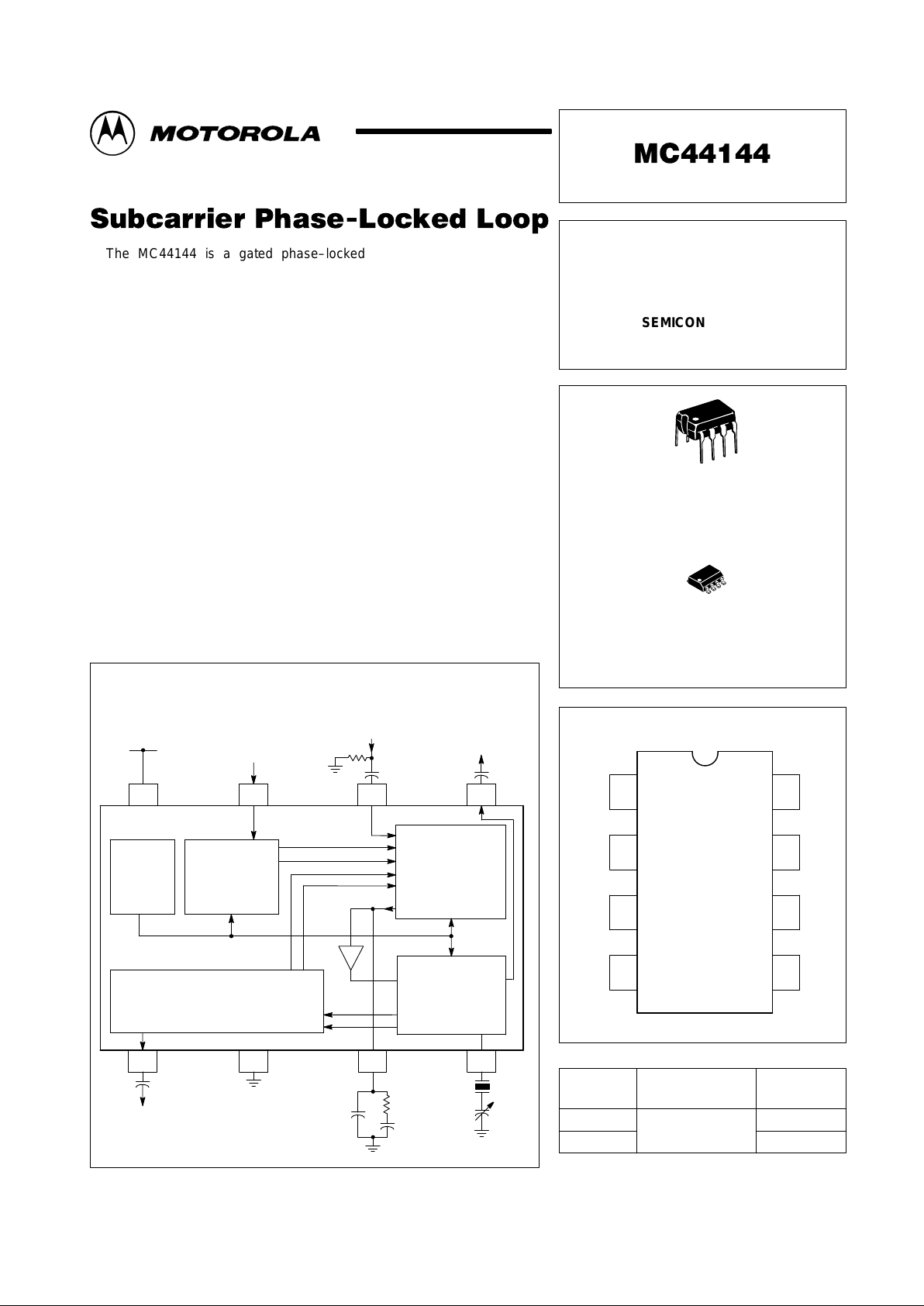
The MC44144 is a gated phase–locked loop intended for, but not
restricted to, video applications. The integrated circuit contains a gated
phase detector, voltage controlled crystal oscillator, divide–by–4 circuitry,
and a video clamp. This device provides a 4X reference frequency output,
and a 1X reference frequency output.
The MC44144 is manufactured using Motorola’s high density, bipolar
MOSAIC process.
• 8–Pin DIP or Surface Mount Package
• Gated–Phase Detector
• Single Pin Voltage Controlled Crystal Oscillator
• 1X and 4X Subcarrier Output
• Operates Off of a Standard 5.0 V Supply
421
567
1.0n
470p
5.0 to 25p
14.32/
17.73MHz
0.1
µ
47k
1.0n0.1
µ
Crystal
Drive
4X Ref
Voltage
Control
Input
Subcarrier
Output
2.6V
Subcarrier
Reference
Output
Gate Pulse
Clamp Out
4X Ref
Out
Phase Det Out
Subcarrier
Reference
Clamp In
Video In
Divide by 4
Video Clamp
Voltage
Reference
VCO
Phase
Detector
4X
Subcarrier
Output
Composite
Video
+ 5.0
Burst
Gate
75
Representative Block Diagram
8
3
Motorola, Inc. 1996 Rev 2
Page 2
MC44144
2
MOTOROLA ANALOG IC DEVICE DATA
ABSOLUTE MAXIMUM RATINGS
Rating Symbol Value Unit
Supply Voltage V
CC
6.0 Vdc
Operating Ambient Temperature T
A
0° to +70 °C
Storage Temperature Range T
stg
– 65 to +150 °C
Operating Junction Temperature T
J
+150 °C
RECOMMENDED OPERATING CONDITIONS
Characteristic Pin Symbol Min Typ Max Unit
Supply Voltage 8 V
CC
4.5 5.0 5.5 Vdc
Composite Video Input (Note 1) 6 mVpp
Burst Amplitude to Acquire Lock – 50 300 1000
NOTE: 1. T otal peak–to–peak voltage of video should not exceed ground or VCC.
ELECTRICAL CHARACTERISTICS (V
CC
= 5.0 Vdc, TA = 25°C)
Characteristic Pin Min Typ Max Unit
Operating Current 8 8.0 10 12 mA
Burst Gate Threshold Voltage: V
IH
7 3.0 – – Vdc
V
IL
– – 1.5
Burst Gate Input Current: IIH (Vin = 5.0 V) – – 20 µA
IIL (Vin = 0 V) – – –0.5
4X Subcarrier 5
Output Voltage: (14.32 MHz) 400 610 650 mVpp
Output Voltage: (17.73 MHz) – 450 –
Output Impedance: (14.3 MHz and 17.73 MHz) – 25 – Ω
Subcarrier Output
Output Voltage: (3.58 MHz and 4.43 MHz) 200 300 400 mVpp
Output Impedance: (3.58 MHz and 4.43 MHz) 1 – 200 – Ω
Phase Angle (Note 1) – –60 – deg
Phase Sensitivity (Notes 1 & 2) – 3.0 – Note 2
Static Phase Error (Note 2) 1, 2 – 3 – deg/100 Hz
Phase–Locked Loop Pull–In Range – ± 350 – Hz
Phase–Locked Loop Hold–In Range – ± 500 –
NOTES: 1. Referenced to composite video input color burst.
NOTES: 2. See paragraph 1 of the Functional Description text.
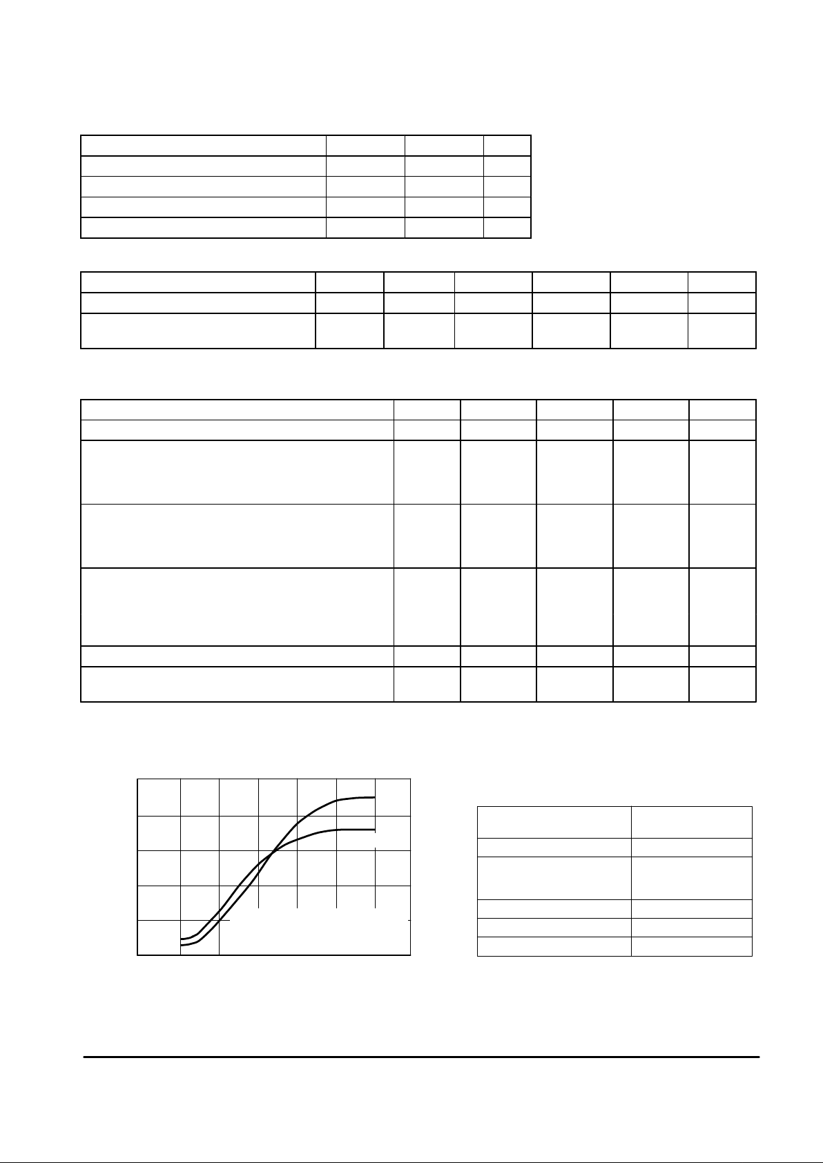
Figure 1. Typical VCXO Gain
VCO CONTROL VOLTAGE (PIN 3 VOLTAGE) (V)
–1.0 0 1.0 2.0 3.0 4.0 5.0 6.0
KO
PAL
4Xf ,
sc
OUTPUT (PIN 5) FREQUENCY (MHz)
FOR PAL
KO
NTSC
4Xf ,
sc
OUTPUT (PIN 5) FREQUENCY (MHz)
FOR NTSC
The gain must be estimated from the
operating point. KO
PAL
is the gain for
PAL applications and KO
NTSC
is the
gain for NTSC applications.
14.322
14.320
14.318
14.316
14.314
14.312
17.745
17.740
17.735
17.730
17.725
17.719
Table 1. Crystal Specifications
Frequency 14.31818 MHz (NTSC)
17.734475 MHz (PAL)
Mode Fundamental
Frequency T olerance
@ 25°C
df/dfo 0°C–70°C
40 ppm
Load Capacitance 20 pF
ESR 50 Ω
C1 (Internal Series Capacitance) 15 mpF
Page 3
MC44144
3
MOTOROLA ANALOG IC DEVICE DATA
Crystal
Drive
4X Ref
Voltage
Control
Input
4X Ref
Out
VCO
1.0k
1.0k
1.0n
1.0n
Subcarrier
Output
4X
Subcarrier
Output
421
567
470p
5.0 to 25p
14.32/
17.73MHz
0.1
µ
47k
0.1
µ
2.6V
Subcarrier
Reference
Output
Gate Pulse
Clamp Out
Phase Det Out
Subcarrier
Reference
Clamp In
Video In
Divide by 4
Video Clamp
Voltage
Reference
Phase
Detector
Composite
Video
+ 5.0
Burst
Gate
75
8
3
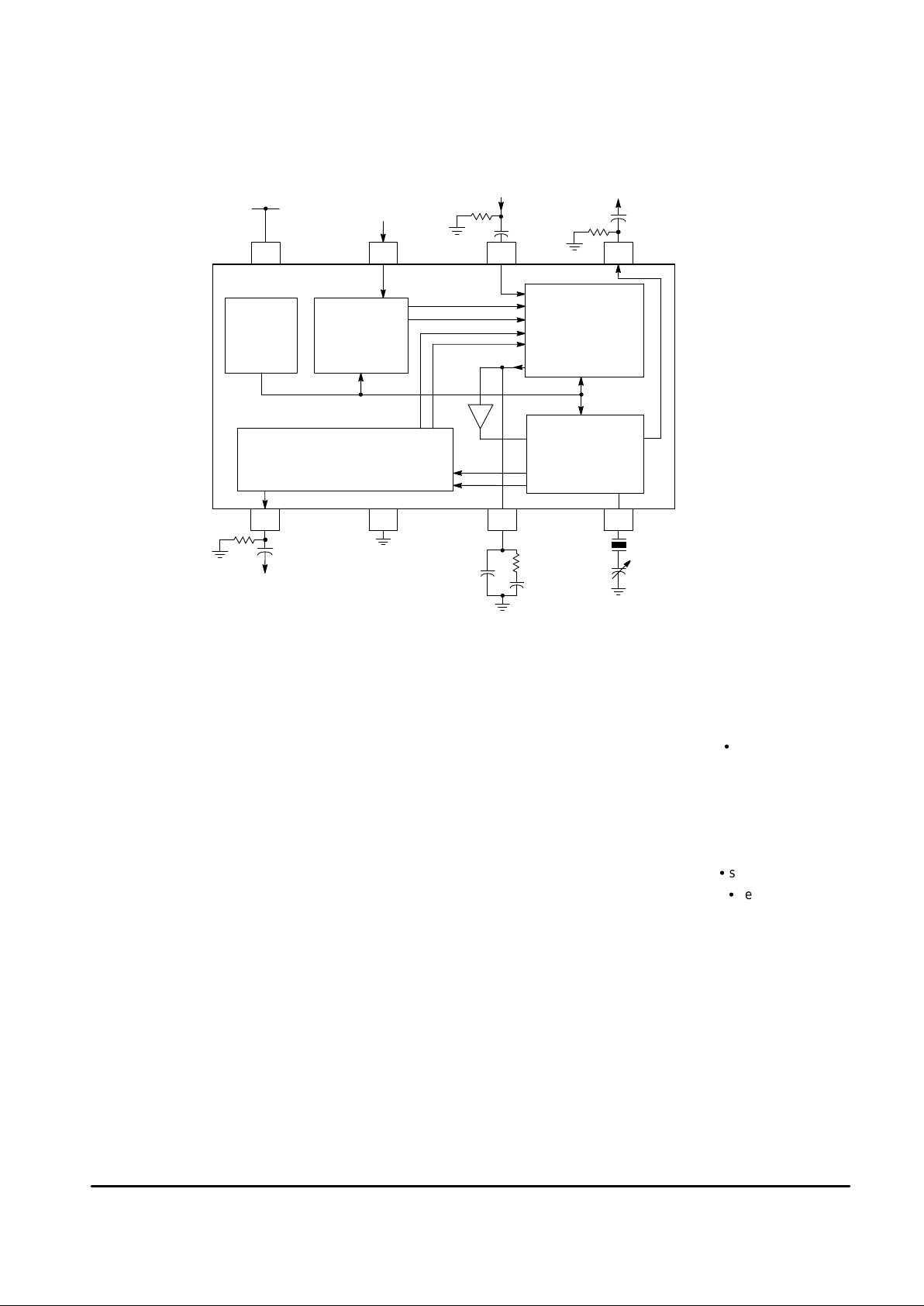
Figure 2. Representative Schematic Diagram
FUNCTIONAL DESCRIPTION
The MC44144 is designed to implement the color sync
function in a video system. When provided NTSC/PAL
composite video or composite chroma and burst gate inputs,
the IC will phase–lock a Voltage Controlled Crystal Oscillator
(VCXO) to the color burst. Both 4X and 1X subcarrier
frequency outputs are provided by the IC. The VCXO
operates off of a 4X subcarrier crystal and The VCXO
operates off a 4X subcarrier crystal and is capable of at least
± 600 Hz of pull–in. The tradeoff for such a wide pull–in range
is a resultant “soft” lock, or a 3° phase shift per 100 Hz
change
in oscillator free–run or input reference frequency.
In addition to providing the gate pulse for the MC44144
phase detector, the Burst Gate input also initiates a clamp
pulse that sets up the level of the composite video at the input
to the Phase Detector. The start and duration of the Gate
Pulse should be timed so that the pulse envelopes the color
burst of the video signal, but not so wide as to gate sync or
video into the Phase Detector.
The Phase Detector is enabled when the voltage at the
Burst Gate input (Pin 7) is above the nominal 2.2 V threshold.
While this makes possible the ability to lock to a color burst,
it does not exclude the possibility of lock to a constant
reference. If a constant source is to be the reference, the
Phase Detector can be permanently enabled by holding the
voltage on the Phase Detector input pin higher than the
threshold voltage.
The phase detector gain must be specified in two ways, for
a constant reference and for a burst–locked application. The
gain in a constant reference application is specified by the
maximum current output with the maximum phase error. For
a maximum phase error of π/2 radians the maximum current
available is approximately 200 µA. So the phase detector
gain is defined as,
KPD = 200/(π/2)(µA/rad S sec)
For a burst–locked application, the Phase Detector is
active for only the duration of the color burst. Therefore the
phase detector gain must be specified as an average gain
over a line period. In this case the phase detector gain for
NTSC and for PAL applications is,
KPD
NTSC
= (8/(π/2))(µA/rad S sec) and,
KPD
PAL
= (7/(π/2))(µA/rad S sec)
A suitable filter for both types of applications is shown in
the test schematic Figure 2. This same filter also works for
both NTSC and PAL applications.
The 4X subcarrier Voltage Controlled Crystal Oscillator
(VCXO) uses a design that enables the use of series or
parallel resonant types of crystals. Still, layout and crystal
positioning are critical as the oscillator frequency is sensitive
to shunt capacitance. Care should be taken to keep the
crystal close to the IC and crystal switching should be
avoided. A suitable parallel type crystal would meet the
specifications in Table 1.
A plot showing the VCXO gain is shown in Figure 1. From
this plot the gain must be estimated from the operating point.
KO
PAL
is the gain for PAL applications and KO
NTSC
is the
gain for NTSC applications.
Page 4

MC44144
4
MOTOROLA ANALOG IC DEVICE DATA
PIN FUNCTION DESCRIPTION
Name Pin Representative Circuitry Description Expected Waveforms
Subcarrier
Output
1
5.0k
200
V
CC
Subcarrier Output. A
phase–locked reference of the
PAL or NTSC color burst is
output at this pin.
A 300 mVpp square wave is output.
Some high frequency content is
present.
Ground 2 Circuit Ground
Phase
Detector
Output
3
1.0k 31k
33k
2.5V
The error current from the
phase detector is output at this
pin. A filter circuit should be
connected at this pin.
A beat waveform, showing both
horizontal period and half the
subcarrier period, is present.
Line Period
1/2 Subcarrier Period
4X Sub Xtal 4
gm
2.0k
400
V
CC
V
ref
gm
Crystal Oscillator Pin. A 4X
subcarrier parallel resonant
crystal, in series with a 5.0 to
25 pF trimmer capacitor
provides the resonant element
for the Voltage Controlled
Crystal Oscillator (VCXO).
Approximately 40 mVpp. A scope
probe will disturb the frequency of
oscillation.
4X Subcarrier
Output (or
Black Burst)
5
5.0k
V
CC
Buffered output from the 4X
voltage controlled oscillator.
The sinusoidal 4Xfsc oscillator output
is available at this pin.
The output is nominally:
525 mVpp for NTSC,
425 mVpp for PAL.
Composite
Video Input
(Black Burst,
Continuous
Wave, or
Composite
Chroma
can also be
applied)
6
22k
V
CC
Composite Video Input. Color
burst from the video present at
this pin is used as a reference
to phase lock the VCXO.
Positive or negative video may
be used.
Composite video should be applied
at this pin. The color burst
amplitude of the input video should
be at least 50 mV , but no more than
1000 mV. The waveform at this pin
should not exceed ground or VCC.
V
CC
GND
2.6V
Burst Gate
Input
7
V
CC
22k
22k
Input for the phase detector
gate pulse. TTL compatible.
The threshold is nominally
2.6V .
A positive going gate pulse should
be applied at this pin. The Burst Gate
input should envelope the color
burst.
Pin 7
2.2V
Pin 6
V
CC
8 Power Supply Pin. 5.0 Vdc
should be applied at this pin.
Page 5

MC44144
5
MOTOROLA ANALOG IC DEVICE DATA
Linear and TTL Output Buffers
The output buffers of the MC44144 are not designed to
any specific logic family. If it is desired, Linear or TTL buffers
can be added externally. Figure 3 shows an example of a
Linear buffer using an MC3346 Transistor array; virtually any
utility transistor can be used. Figure 4 shows a TTL type
buffer using an MC74LS04 buffer.
Figure 3. Linear Buffer
Figure 4. TTL Buffer
MC3346
TTL Output
4X Subcarrier
Output or 1X
Subcarrier
Output
MC74LS04
12
10
8
6
4
2
13
11
9
5
3
1
R
3
1.0k
C
1
0.01
µ
F
R
2
10k
C
2
47pF
4X Subcarrier
Output or 1X
Subcarrier
Output
C
in
1000
µ
F
R
2
1.8k
R
1
3.3k
14
13
12
11
10
9
8
1
2
3
4
5
6
7
C
2
100pF
R
3
300
R
4
430
C
o
1000
µ
F
R
5
56
Linear Output
+5.0V +5.0V
Page 6

MC44144
6
MOTOROLA ANALOG IC DEVICE DATA
P SUFFIX
PLASTIC PACKAGE
CASE 626–05
D SUFFIX
PLASTIC PACKAGE
CASE 751–03
(SO–8)
OUTLINE DIMENSIONS
NOTES:
1. DIMENSION L TO CENTER OF LEADS WHEN
FORMED PARALLEL.
2. PACKAGE CONTOUR OPTIONAL (ROUND OR
SQUARE CORNERS).
3. DIMENSIONING AND TOLERANCING PER ANSI
Y14.5M, 1982.
4. 626–03 AND 626–04 OBSOLETE, NEW STANDARD
626–05.
MIN MINMAX MAX
MILLIMETERS INCHES
DIM
9.40
6.10
3.94
0.38
1.02
0.76
0.20
2.92
–
0.76
10.16
6.60
4.45
0.51
1.78
1.27
0.30
3.43
0.370
0.240
0.155
0.015
0.040
0.030
0.008
0.115
–
0.030
0.400
0.260
0.175
0.020
0.070
0.050
0.012
0.135
10
°
1.01
2.54 BSC
7.62 BSC
0.100 BSC
0.300 BSC
A
B
C
D
F
G
H
J
K
L
M
N
10
°
0.040
F
H
G
D
N
C
K
M
J
L
NOTE 2
14
58
T
φ
0.13 (0.005)
AB
M M M
–A
–
–B
–
–T
–
SEATING
PLANE
MIN MINMAX MAX
MILLIMETERS INCHES
DIM
A
B
C
D
F
G
J
K
M
P
R
4.80
3.80
1.35
0.35
0.40
0.18
0.10
0
°
5.80
0.25
5.00
4.00
1.75
0.49
1.25
0.25
0.25
7
°
6.20
0.50
0.189
0.150
0.054
0.014
0.016
0.007
0.004
0
°
0.229
0.010
0.196
0.157
0.068
0.019
0.049
0.009
0.009
7
°
0.244
0.019
1.27 BSC 0.050 BSC
NOTES:
1. DIMENSIONS “A” AND “B” ARE DATUMS AND “T”
IS A DATUM SURFACE.
2. DIMENSIONING AND TOLERANCING PER ANSI
Y14.5M, 1982.
3. CONTROLLING DIM: MILLIMETER.
4. DIMENSION “A” AND “B” DO NOT INCLUDE
MOLD PROTRUSION.
5. MAXIMUM MOLD PROTRUSION 0.15 (0.006)
PER SIDE.
6. 751–01 AND –02 OBSOLETE, NEW STANDARD
751–03.
–A
–
–B
–
P
1
4
58
G
C
SEATING
PLANE
D
8 PL
K
–T
–
R X 45°
M
F
J
4 PL
0.25 (0.010) T B A
M
S S
0.25 (0.010)
B
M M
Page 7

MC44144
7
MOTOROLA ANALOG IC DEVICE DATA
Motorola reserves the right to make changes without further notice to any products herein. Motorola makes no warranty , representation or guarantee regarding
the suitability of its products for any particular purpose, nor does Motorola assume any liability arising out of the application or use of any product or circuit, and
specifically disclaims any and all liability, including without limitation consequential or incidental damages. “T ypical” parameters which may be provided in Motorola
data sheets and/or specifications can and do vary in different applications and actual performance may vary over time. All operating parameters, including “Typicals”
must be validated for each customer application by customer’s technical experts. Motorola does not convey any license under its patent rights nor the rights of
others. Motorola products are not designed, intended, or authorized for use as components in systems intended for surgical implant into the body, or other
applications intended to support or sustain life, or for any other application in which the failure of the Motorola product could create a situation where personal injury
or death may occur. Should Buyer purchase or use Motorola products for any such unintended or unauthorized application, Buyer shall indemnify and hold Motorola
and its officers, employees, subsidiaries, affiliates, and distributors harmless against all claims, costs, damages, and expenses, and reasonable attorney fees
arising out of, directly or indirectly, any claim of personal injury or death associated with such unintended or unauthorized use, even if such claim alleges that
Motorola was negligent regarding the design or manufacture of the part. Motorola and are registered trademarks of Motorola, Inc. Motorola, Inc. is an Equal
Opportunity/Affirmative Action Employer.
Page 8

MC44144
8
MOTOROLA ANALOG IC DEVICE DATA
How to reach us:
USA/EUROPE /Locations Not Listed: Motorola Literature Distribution; JAPAN: Nippon Motorola Ltd.; Tatsumi–SPD–JLDC, 6F Seibu–Butsuryu–Center,
P.O. Box 20912; Phoenix, Arizona 85036. 1–800–441–2447 or 602–303–5454 3–14–2 Ta tsumi Koto–Ku, Tokyo 135, Japan. 03–81–3521–8315
MFAX: RMF AX0@email.sps.mot.com – TOUCHT ONE 602–244–6609 ASIA/PACIFIC: Motorola Semiconductors H.K. Ltd.; 8B Tai Ping Industrial Park,
INTERNET: http://Design–NET.com 51 Ting Ko k Road, Tai Po, N.T ., Hong Kong. 852–26629298
MC44144/D
*MC44144/D*
◊
 Loading...