

Page 1
MC44107MOTOROLA
1
Product Preview
CMOS
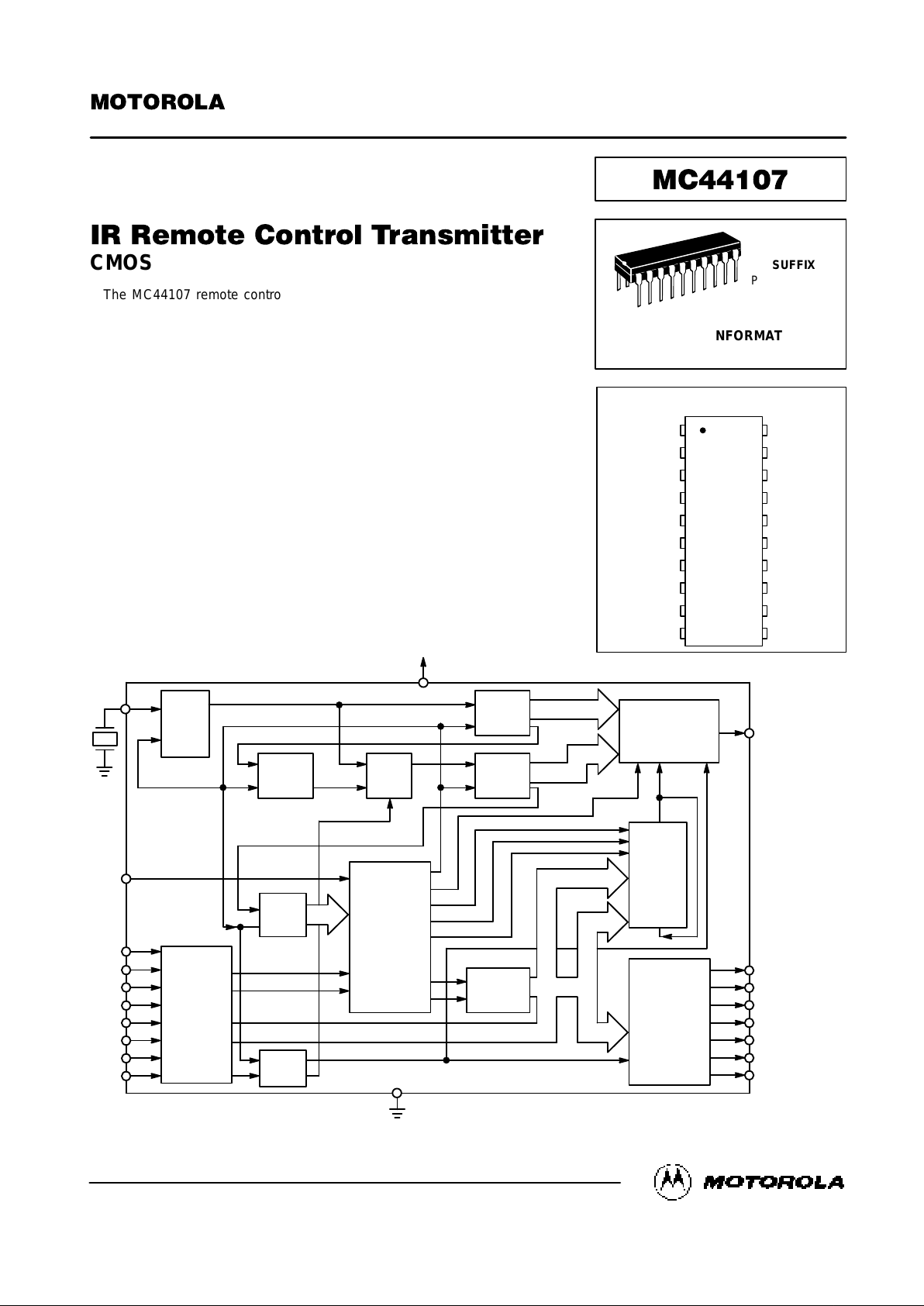
The MC44107 remote control transmitter converts a keyboard input into a
pulse code modulated signal suitable for infrared transmission to an appropriate
receiver. Its large command capacity, 512 commands, makes it highly suited to
remote control applications in TV, video, hi–fi, etc. The transmitter is an LSI
circuit realized in complementary MOS technology.
• Binary Coded, 9–Bit PCM Data Word
• Simple Modulator Requirements
• One–Pin Reference Oscillator for External Ceramic Resonator
• Very Low (Maximum 1 µA) Standby Current Consumption
• Wide Operating Voltage Range: 4 to 10 V
• Operating Temperature Range: – 40 to 85° C
CB
CC
CD
CE
CF
CG
CH
14
15
19
13
18
16
12
MODULATOR
9–BIT
SHIFT
REG.
COLUMN
DECODER
SCANNER
4
DATA
MUX
÷
2
4
÷
2
5
SUPERVISE
AND
CONTROL
÷
2
2
ROW
ENCODER
TEST
÷
2
5
R1
R2
R3
R4
R5
R6
R7
R8
5
2
9
8
1
6
3
7
OSC
OSC
PAGE
11
V
DD
20
V
SS
BLOCK DIAGRAM
17
10
This document contains information on a product under development. Motorola reserves the right to change or discontinue this product without notice.
Order this document
by MC44107/D
SEMICONDUCTOR TECHNICAL DATA
P SUFFIX
PLASTIC DIP
CASE 738
ORDERING INFORMATION
MC44107P Plastic DIP
PIN ASSIGNMENT
R6
D
out
R7
R2
R5
V
SS
R3
R4
R8
R1 5
4
3
2
1
10
9
8
7
6
14
15
16
17
18
19
20
11
12
13
CG
OSC
CF
CD
MUX
PAGE
CH
CE
CC
CB
20
1
Motorola, Inc. 1995
REV 2
8/95
Page 2
MC44107 MOTOROLA
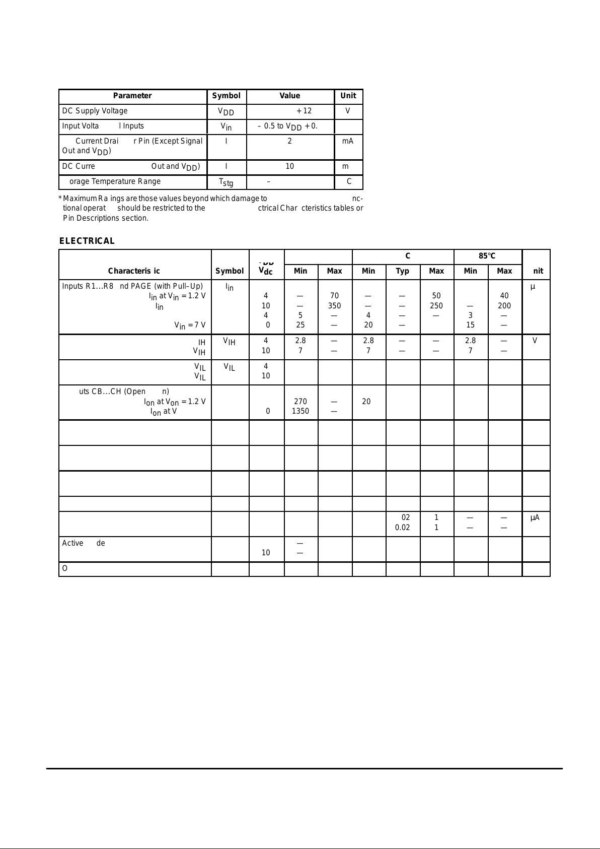
2
MAXIMUM RATINGS* (Voltages referenced to V
SS
)
Parameter
Symbol
Value
Unit
DC Supply Voltage
V
DD
– 0.5 to + 12
V
Input Voltage, All Inputs
V
in
– 0.5 to VDD + 0.5
V
DC Current Drain per Pin (Except Signal
Out and VDD)
I
2
mA
DC Current Drain (Signal Out and VDD)
I
10
mA
Storage Temperature Range
T
stg
– 65 to + 150
°C
*Maximum Ratings are those values beyond which damage to the device may occur. Func-
tional operation should be restricted to the limits in the Electrical Characteristics tables or
Pin Descriptions section.
ELECTRICAL CHARACTERISTICS
V
– 40°C 25°C 85°C
Characteristic
Symbol
V
DD
V
dc
Min Max Min Typ Max Min Max
Unit
Inputs R1…R8 and PAGE (with Pull–Up)
Iin at Vin = 1.2 V
Iin at Vin = 3 V
Iin at Vin = 2.8 V
Iin at Vin = 7 V
I
in
4
10
4
10
—
—
5
25
70
350
—
—
—
—
4
20
—
—
—
—
50
250
—
—
—
—
3
15
40
200
—
—
µA
V
IH
V
IH
V
IH
4
10
2.8
7
—
—
2.8
7
—
—
—
—
2.8
7
—
—
V
V
IL
V
IL
V
IL
4
10
—
—
1.2
3
—
—
—
—
1.2
3
—
—
1.2
3
V
Outputs CB…CH (Open Drain)
Ion at Von = 1.2 V
Ion at Von = 3 V
I
on
4
10
270
1350
—
—
200
1000
—
—
—
—
160
800
—
—
µA
I
off
I
off
I
off
4
10
—
—
1
1
—
—
1
1
—
—
—
—
1
1
µA
Output DATA VOH at I
source
= 1.0 mA V
OH
4
10
3.2
9.6
—
—
3.0
9.5
—
—
1
0.5
2.8
9.4
—
—
V
VOL at I
sink
= 1.0 mA V
OL
4
10
—
—
0.8
0.4
—
—
—
—
1
0.5
—
—
1.2
0.6
V
Supply Voltage V
DD
— 4 10 4 — 10 4 10 V
Standby Current I
DDSTB
4
10
—
—
—
—
—
—
0.02
0.02
1
1
—
—
—
—
µA
Active Mode Current I
DDACT
4
10
—
—
—
—
—
—
0.07
0.45
1
2
—
—
—
—
mA
Oscillator Frequency f
osc
— — — 430 — 530 — — kHz
This device contains protection circuitry to
guard against damage due to high static
voltages or electric fields; however, it is advised that precautions be taken to avoid
application of voltage higher than maximum
rated voltages to this high–impedance circuit.
For proper operation it is recommended that
Vin and V
out
be constrained to the range VSS ≤
(Vin or V
out
) ≤VDD.
Unused inputs must always be tied to an
appropriate logic voltage level (e.g., either V
SS
or VDD).
Page 3

MC44107MOTOROLA
3
CIRCUIT OPERATION
The transmitter emits a 9–bit, labelled A (LSB) to I (MSB),
binary code able to encode 512 commands organized as
8 pages of 64 commands. All of these commands are user
selectable except the last command (511) which is used as
an SST, Start/Stop Transmission code.
Each bit of the transmitted signal is in the form of a biphase
pulse code modulated (PCM) signal, whose coding is shown
in Figure 1.
Figure 1. Signal Coding
BIT–n
‘0’
AM
‘1’
f1*
f1*
*f1 is a train of pulses at the
carrier frequency ÷ 16.
The keyboard can be a simple switch matrix, connected
between the eight row inputs (1 to 8) and the seven column
outputs (B to H). VSS acts as the eight column line to give the
full complement of 64 commands per page. The maximum
“ON” resistance of the keyboard must be limited to 500 Ω.
Page access is accomplished by connecting, by means of
a key, the page input to one of the seven column outputs or
by leaving the input circuit open.
One of the circuit’s major features is its low standby current consumption — typically less than 1 µA. For this reason
the battery may be left continuously in circuit.
As soon as a key is selected, the circuit switches to its active mode and enables the oscillator. To allow for accidental
activation and/or key bounce, the circuit requires that the key
is held for a minimum delay of t
key
, which in the case of a
500 kHz oscillator is 65.6 ms. After this delay the column/
row/page command, consisting of a string of messages (see
Figure 2), appropriate to the key selected will be transmitted
and repeated until the key is released.
Any page key required must be selected before, and held
during, the selection of the column/row matrix key. If this sequence is not followed, the circuit will default to the appropriate command between 0 and 63. If two or more page keys
are accidentally held down, only the first one pressed will be
detected.
A command consists of several messages. Each command starts with the message 511 (SST) followed by the
message appropriate to the key selected. These messages
are repeated until the key is released. The final message is
always followed by the SST message, 511.
Every message consists of a pre–bit, a pre–bit pause, a
start–bit, and nine data bits, where the pre–bit and the start–
bit are always logical “1”. The pre–bit allows for the set up of
the AGC loop in the receiving preamplifier. The truth tables
for data bits are given in Tables 1 and 2, while Figure 2
shows the timing relationships between the commands,
messages, and modulation.
In the event of accidental multi–key operation, the circuit
will react in one of three ways, depending on the combination
of the keys selected.
When two or more keys are connected to the same row input and any column output except A, the command appropriate to the first key selected will be transmitted until that key is
released. After the SST code has been transmitted, assuming another key is still selected, the command appropriate to
that key will be transmitted. If the other key has been released in the meantime, the circuit will revert to standby.
If two keys are selected in the same row with one being
connected to column A, any transmission will terminate with
the SST code and then the circuit will transmit the command
appropriate to the key connected to column A.
In the case where two or more keys connected to the same
column are selected, the circuit reacts in a normal manner to
the first key activated. Upon selection of the second key, the
SST code is transmitted and the circuit will revert to the
standby mode. Only when the multi–key condition is released and a single key is selected will the circuit resume operation, as previously described.
Page 4

MC44107 MOTOROLA
4
MESSAGE TIMING
MODULATION OF BURST
D(1) E(0) F(0) G(1) H(1) I(1)S = 1 A(0) B(1) C(1)
g
h i
f e
d
a b c
e
ddd
SST COM COM COM SSTCOM
COMMAND TIMING
CIRCUIT TIMING*
Modulation a = 4/f
osc
b = 16/f
osc
c = 4/f
osc
d = 256/f
osc
8 µs
32 µs
8 µs
512 µs
1/f Carrier
Half–Bit Time
Message Timing d = 256/f
osc
e = 512/f
osc
f = 1536/f
osc
512 µs
1.02 ms
3.072 ms
Half–Bit Time
Bit Time
Pre–Pulse Time
Command Timing g = 32 x Bit Time
h = 128 x Bit Time
i = 128 x Bit Time
t
key
= 64 x Bit Time
32.8 ms
131 ms
131 ms
65.6 ms
*Times indicated are typical and refer to an oscillator frequency of 500 kHz.
Figure 2. MC44107 Remote Control Transmitter Timing Diagram
Page 5

MC44107MOTOROLA
5
PAGE
CB
COLUMN
OUTPUTS
CH
R1
ROW
INPUTS
R8
DATA
V
DD
OSC
V
SS
DRIVER IC
IR
DIODES
1000 µF
CERAMIC
RESONATOR
PAGE KEYS
MATRIX
KEYS
Figure 3. Transmitter Circuit
MC44107
Page 6

MC44107 MOTOROLA
6
PIN DESCRIPTIONS
ROW INPUTS
1 to 8 ( Pins 1, 2, 3, and 5 – 9) In the standby mode these
inputs are held high by internal pull–up resistors. As soon as
a key is pressed, a logical “0” is presented by the column output on that particular line. This switches the circuit to the active mode and starts the oscillator.
COLUMN OUTPUTS
B to H (Pins 12 – 16, 18, and 19) In the standby mode
these pins are held low, logical “0”. When a key is selected
and the oscillator starts, the outputs are released and the
scanning routine starts.
PAGE INPUT
(Pin 11) This input is connected directly to the transmitter’s
supervisory and control circuitry and may be connected to
one of the column outputs, via a key , or left open. If the pin is
left open, the first page of 64 commands will be available
(see Table 1). If connected to one of the column outputs, the
remaining pages become available (see Table 2). The specified standby current consumption is maintained regardless of
the load applied to the input: 0 V < V page < V
DD.
OSCILLATOR
(Pin 17) A one–pin oscillator is incorporated into the circuit,
which has been specifically designed for use with an inexpensive ceramic resonator between 430 kHz and 530 kHz. It
is possible to use a tuned LC circuit with a series capacitor, in
place of the ceramic resonator.
DATA OUTPUT
(Pin 4) This output provides the modulated signal for subsequent external amplification.
SPECIAL NOTE: KEYBOARD
It is important, when considering a keyboard, that the maximum “ON” resistance, even after aging, of 500 Ω is strictly
observed.
Page 7

MC44107MOTOROLA
7
Table 1. Transmitted Codes
Matrix
Binary Code
Matrix
Binary Code
Message
Number
Connect
Row/Col
A B C D E F G H I
Message
Number
Connect
Row/Col
A B C D E F G H I
0 1A 0 0 0 0 0 0 0 0 0 32 5A 0 0 0 0 0 1 0 0 0
1 1B 1 0 0 0 0 0 0 0 0 33 5B 1 0 0 0 0 1 0 0 0
2 1C 0 1 0 0 0 0 0 0 0 34 5C 0 1 0 0 0 1 0 0 0
3 1D 1 1 0 0 0 0 0 0 0 35 5D 1 1 0 0 0 1 0 0 0
4 1E 0 0 1 0 0 0 0 0 0 36 5E 0 0 1 0 0 1 0 0 0
5 1F 1 0 1 0 0 0 0 0 0 37 5F 1 0 1 0 0 1 0 0 0
6 1G 0 1 1 0 0 0 0 0 0 38 5G 0 1 1 0 0 1 0 0 0
7 1H 1 1 1 0 0 0 0 0 0 39 5H 1 1 1 0 0 1 0 0 0
8 2A 0 0 0 1 0 0 0 0 0 40 6A 0 0 0 1 0 1 0 0 0
9 2B 1 0 0 1 0 0 0 0 0 41 6B 1 0 0 1 0 1 0 0 0
10 2C 0 1 0 1 0 0 0 0 0 42 6C 0 1 0 1 0 1 0 0 0
11 2D 1 1 0 1 0 0 0 0 0 43 6D 1 1 0 1 0 1 0 0 0
12 2E 0 0 1 1 0 0 0 0 0 44 6E 0 0 1 1 0 1 0 0 0
13 2F 1 0 1 1 0 0 0 0 0 45 6F 1 0 1 1 0 1 0 0 0
14 2G 0 1 1 1 0 0 0 0 0 46 6G 0 1 1 1 0 1 0 0 0
15 2H 1 1 1 1 0 0 0 0 0 47 6H 1 1 1 1 0 1 0 0 0
16 3A 0 0 0 0 1 0 0 0 0 48 7A 0 0 0 0 1 1 0 0 0
17 3B 1 0 0 0 1 0 0 0 0 49 7B 1 0 0 0 1 1 0 0 0
18 3C 0 1 0 0 1 0 0 0 0 50 7C 0 1 0 0 1 1 0 0 0
19 3D 1 1 0 0 1 0 0 0 0 51 7D 1 1 0 0 1 1 0 0 0
20 3E 0 0 1 0 1 0 0 0 0 52 7E 0 0 1 0 1 1 0 0 0
21 3F 1 0 1 0 1 0 0 0 0 53 7F 1 0 1 0 1 1 0 0 0
22 3G 0 1 1 0 1 0 0 0 0 54 7G 0 1 1 0 1 1 0 0 0
23 3H 1 1 1 0 1 0 0 0 0 55 7H 1 1 1 0 1 1 0 0 0
24 4A 0 0 0 1 1 0 0 0 0 56 8A 0 0 0 1 1 1 0 0 0
25 4B 1 0 0 1 1 0 0 0 0 57 8B 1 0 0 1 1 1 0 0 0
26 4C 0 1 0 1 1 0 0 0 0 58 8C 0 1 0 1 1 1 0 0 0
27 4D 1 1 0 1 1 0 0 0 0 59 8D 1 1 0 1 1 1 0 0 0
28 4E 0 0 1 1 1 0 0 0 0 60 8E 0 0 1 1 1 1 0 0 0
29 4F 1 0 1 1 1 0 0 0 0 61 8F 1 0 1 1 1 1 0 0 0
30 4G 0 1 1 1 1 0 0 0 0 62 8G 0 1 1 1 1 1 0 0 0
31 4H 1 1 1 1 1 0 0 0 0 63 8H 1 1 1 1 1 1 0 0 0
Page 8

MC44107 MOTOROLA
8
Table 2. Page Table
Message
Page Input
Connected To
G H I
0 to 63 Not Connected 0 0 0
64 to 127 CB 1 0 0
128 to 191 CC 0 1 0
192 to 255 CD 1 1 0
256 to 319 CE 0 0 1
320 to 383 CF 1 0 1
384 to 447 CG 0 1 1
448 to 511 CH 1 1 1
PACKAGE DIMENSIONS
P SUFFIX
PLASTIC DIP
CASE 738–03
1.070
0.260
0.180
0.022
0.070
0.015
0.140
15
°
0.040
1.010
0.240
0.150
0.015
0.050
0.008
0.110
0
°
0.020
25.66
6.10
3.81
0.39
1.27
0.21
2.80
0
°
0.51
27.17
6.60
4.57
0.55
1.77
0.38
3.55
15
°
1.01
0.050 BSC
0.100 BSC
0.300 BSC
1.27 BSC
2.54 BSC
7.62 BSC
MIN MINMAX MAX
INCHES MILLIMETERS
DIM
A
B
C
D
E
F
G
J
K
L
M
N
NOTES:
1. DIMENSIONING AND TOLERANCING PER ANSI
Y14.5M, 1982.
2. CONTROLLING DIMENSION: INCH.
3. DIMENSION L TO CENTER OF LEAD WHEN
FORMED PARALLEL.
4. DIMENSION B DOES NOT INCLUDE MOLD
FLASH.
-A-
C
K
N
E
G F
D
20 PL
J 20 PL
L
M
-T-
SEATING
PLANE
1 10
1120
0.25 (0.010) T A
M M
0.25 (0.010) T B
M M
B
Motorola reserves the right to make changes without further notice to any products herein. Motorola makes no warranty , representation or guarantee regarding
the suitability of its products for any particular purpose, nor does Motorola assume any liability arising out of the application or use of any product or circuit,
and specifically disclaims any and all liability, including without limitation consequential or incidental damages. “T ypical” parameters can and do vary in different
applications. All operating parameters, including “T ypicals” must be validated for each customer application by customer’s technical experts. Motorola does
not convey any license under its patent rights nor the rights of others. Motorola products are not designed, intended, or authorized for use as components in
systems intended for surgical implant into the body, or other applications intended to support or sustain life, or for any other application in which the failure of
the Motorola product could create a situation where personal injury or death may occur. Should Buyer purchase or use Motorola products for any such
unintended or unauthorized application, Buyer shall indemnify and hold Motorola and its officers, employees, subsidiaries, affiliates, and distributors harmless
against all claims, costs, damages, and expenses, and reasonable attorney fees arising out of, directly or indirectly, any claim of personal injury or death
associated with such unintended or unauthorized use, even if such claim alleges that Motorola was negligent regarding the design or manufacture of the part.
Motorola and are registered trademarks of Motorola, Inc. Motorola, Inc. is an Equal Opportunity/Affirmative Action Employer.
How to reach us:
USA/EUROPE: Motorola Literature Distribution; JAPAN: Nippon Motorola Ltd.; Tatsumi–SPD–JLDC, Toshikatsu Otsuki,
P.O. Box 20912; Phoenix, Arizona 85036. 1–800–441–2447 6F Seibu–Butsuryu–Center, 3–14–2 Tatsumi Koto–Ku, Tokyo 135, Japan. 03–3521–8315
MFAX: RMFAX0@email.sps.mot.com – TOUCHTONE (602) 244–6609 HONG KONG: Motorola Semiconductors H.K. Ltd.; 8B Tai Ping Industrial Park,
INTERNET: http://Design–NET.com 51 Ting Kok Road, Tai Po, N.T., Hong Kong. 852–26629298
MC44107/D
*MC44107/D*
◊
 Loading...