

Page 1
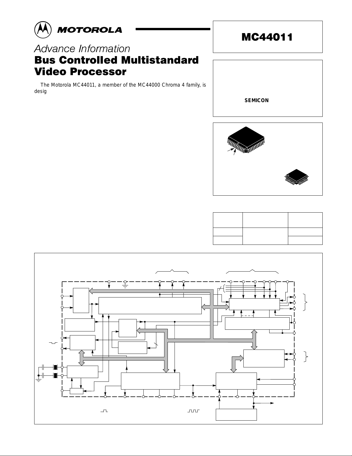
The Motorola MC44011, a member of the MC44000 Chroma 4 family, is
designed to provide RGB or YUV outputs from a variety of inputs. The inputs
can be composite video (two inputs), S–VHS, RGB, and color difference
(R–Y, B–Y). The composite video can be PAL and/or NTSC as the MC44011
is capable of decoding both systems. Additionally , R–Y and B–Y outputs and
inputs are provided for use with a delay line where needed. Sync separators
are provided at all video inputs.
In addition, the MC44011 provides a sampling clock output for use by a
subsequent triple A/D converter system which digitizes the RGB/YUV
outputs. The sampling clock (6.0 to 40 MHz) is phase–locked to the
horizontal frequency.
Additional outputs include composite sync, vertical sync, field
identification, luma, burst gate, and horizontal frequency.
Control of the MC4401 1, and reading of status flags, is via an I2C bus.
• Accepts NTSC and PAL Composite Video, S–VHS, RGB, and R–Y, B–Y
• Includes Luma and Chroma Filters, Luma Delay Lines, and Sound Traps
• Digitally Controlled via I
• R–Y, B–Y Inputs for Alternate Signal Source
• Line–Locked Sampling Clock for A/D Converters
• Burst Gate, Composite Sync, Vertical Sync and Field Identification Outputs
• RGB/YUV Outputs can Provide 3.0 Vpp for A/D Inputs
• Overlay Capability
• Single Power Supply: 5.0 V, ±5%, 550 mW (Typical)
• 44 Pin PLCC and QFP Packages
2
C Bus
BUS CONTROLLED
MULTISTANDARD
VIDEO PROCESSOR
44
1
FB SUFFIX
PLASTIC PACKAGE
CASE 824E
ORDERING INFORMATION
Device
MC44011FN
MC44011FB
Order this document by MC44011/D
SEMICONDUCTOR
TECHNICAL DATA
FN SUFFIX
PLASTIC PACKAGE
CASE 777
(PLCC)
44
(QFP)
Operating
Temperature Range
TA = 0° to +70°C
1
Package
PLCC–44
QFP
Comp
Video 1
Comp
Video 2
Vertical
Output
Field ID
17.7 MHz
14.3 MHz
Filter
Input
Select
Sync
Separator
Vertical
Decoder
Oscillator
PLL
CC1
Burst
Gate
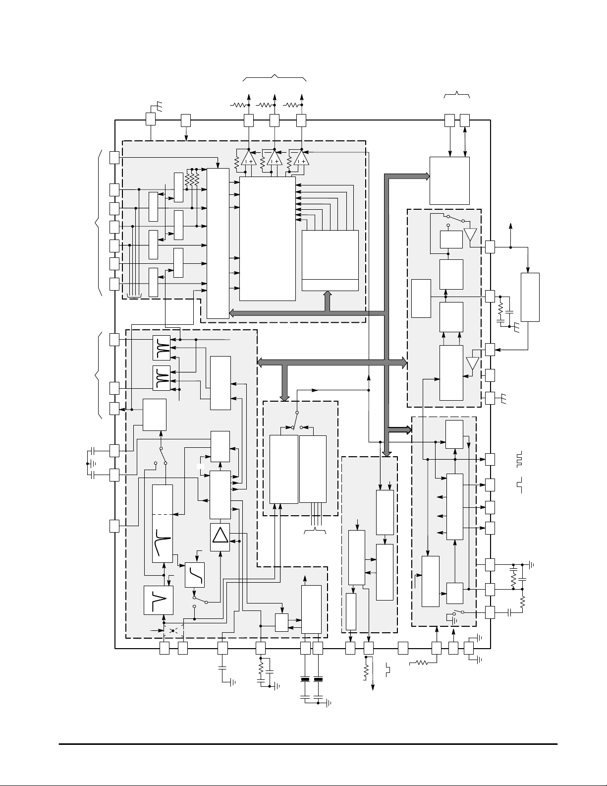
Representative Block Diagram
Outputs
Gnd1V
Sound Trap/Luma Filter/Luma Delay/
Chroma Filter/P AL and NTSC
Decoder/Hue and Saturation Control
Select
Sync
Separator
16Fh/
C
Sync
PLL #1 Horizontal
Filter
Switch
4
PLL/VCO
H
Filter
B–YR–YY1
Quiet
Gnd
MC44011
Fh
Ref
4
15 k
Ret
R–Y
Data Bus
PLL #2
Pixel Clock
PLL/VCO
Frequency
Divider
Inputs
Y2
B–Y
Color Difference
Stage
Contrast, Brightness,
Saturation Control DACs
Interface/
Registers
PLL
Filter
G
R
I2C Data
Clock
B
Fast
Comm
R/V
G/Y
B/U
V
CC2
Gnd2
SDL
SCL
V
CC3
Gnd3
To A/D Converters
Outputs
µ
P
To
This document contains information on a new product. Specifications and information herein
are subject to change without notice.
MOTOROLA ANALOG IC DEVICE DATA
Motorola, Inc. 1996 Rev 1
1
Page 2
MC44011
Inputs
Outputs
R/V
5.0
5.0
20
Color Matrix and
Blank
Burst
Clamp Clamp Clamp
Gate
CC2
V
(5.0 V)
23
ClampClampClamp
Signal Selection
B–YY R–Y B G R
Gnd2
24
25282726293031424133324334
Sep
T o Sync
G/Y
5.0
21
Controls
B/U
22
Contrast
Saturation
Red Gain
Blue Gain
Brightness
∆
∆
DACs
Color Difference Stage
Red DC
Blue DC
∆
∆
2Fo
Bus Control & Flag Status Read
Voltage
Monitor
SCL
5
C Data
2
Interface/
I
Fo
2
÷
VCO
12–40 MHz
Pump
Charge
U
D
P
µ
To
SDL
6
Registers
T o A/D Converters
Clock
PLL #2
Filter
Ret
15 k
Divider
Frequency
R–Y
B–Y
Hue DACs
C
Saturation/
Outputs
Fs Notch
X1, X2, X8
Delay
Adj. Luma
Figure 1. Representative Block Diagram
Y1
Clamp Y1 B–Y R–Y R–Y B–Y Y2 B G R FC
Ident
Filter
Select
System
Luma
4.4/4.8/5.2
5.5/6.0/6.5 MHz
Select
Delay
1
Comp Video 1
Luma Peaking
Chroma Trap &
C
Sound Trap
3
Comp Video 2
Ident
C
Decoder
PAL/NTSC
C
Chroma Filter
2
ACC Filter
R–Y
B–Y
Separator &
Adaptive Sync
ACC
PAL/NTSC/S–VHS Decoder
PLL
44
Chroma PLL Filter
Selector
Sync Separator
From
C
Oscillator
38
Xtal 1
17.7 MHz
Sync Separator
& Selector
Inputs
RGB & Y2
36
Xtal 2
14.3 MHz
Comp Sync
Vertical Decoder
2Fh
Vert. Sync
525, 625
& Decoder
Line Counter
Coincidence
Field ID
7
4
Field ID
Vertical Sync
5.0 V
16Fh
Separator
Counter
37
NC
5.0
PLL #2
PLL #1
C
ref
I
Comparator
Phase & Frequency
Det
Phase
64
÷
16Fh Blank 2Fh
Circuit
Calibration
VCO
9
40
CC1
V
(5.0 V)
Figure 1.
39
Gnd1
12 11 10 13 35 8 14 17 19 15 16 18
CC3
V
Gnd3
Fh
S/C Burst
16Fh/
Quiet
H Fil
H Filt
(5.0 V)
Ref
Gate
Sync
C
GND
Switch
2
MOTOROLA ANALOG IC DEVICE DATA
Page 3
MC44011
ELECTRICAL CHARACTERISTICS (The tested electrical characteristics are based on the conditions shown in Table 1 and 2.
Composite Video input signal = 1.0 Vpp, composed of: 0.7 Vpp Black–to–White; 0.3 Vpp Sync–to–Black; 0.3 Vpp Color Burst. V
= V
CC3
= 5.0 V, I
= 32 µA (Pin 9), unless otherwise noted.)
ref
Table 1. Control Bit Test Settings
Control Bit Name Value Function
$77–7 S–VHS–Y 0 Composite Video input selected.
$77–6 S–VHS–C 0 Composite Video input selected.
$77–5 FSI 0 50 Hz Field Rate selected.
$77–4 L2 GATE 0 PLL #2 Gating enabled.
$77–3 BLCP 0 Clamp Pulse Gating enabled.
$77–2 L1 GATE 0 Vertical Gating enabled.
$77–1, 0 CB1, CA1 1,1 Vertical section Auto–Countdown mode
$78–7 36/68 µs 0 Time from beginning of Line 4 to V ertical Sync is 36 µs.
$78–6 CalKill 0 Horizontal Calibration Loop enabled.
$79–7, 6 HI, VI 1,1 Normal
$7A–7 Xtal – 0 = 17.7 MHz crystal selected, 1 = 14.3 MHz crystal selected.
$7A–6 SSD 0 Normal
$7B–7, 6 T1, T2 1,1 Sound Trap Notch filter set to 5.5 MHz (with 17.7 MHz crystal).
$7C–7 SSC 0 Permits PAL and NTSC selection.
$7C–6, $7D–6 SSA, SSB – 0, 1 = PAL decoding, 1,0 = NTSC decoding
$7D–7, $7E–7, 6 P1, P3, P2 1, 1, 1 Sets Luma Peaking at 0 dB.
$7F–7, 6, $80–6 D3, D1, D2 0, 0, 0 Set Luma Delay to minimum
$80–7 RGB EN 0 Fast Commutate input can enable RGB inputs.
$81–7 Y2 EN 0 Y2 input (Pin 29) deselected
$81–6 Y1 EN 1 Y1 luma path from PAL/NTSC decoder selected.
$82–7 YUV EN 0 RGB output mode selected
$82–6 YX EN 0 Disable luma matrix from RGB inputs.
$83–7 L2 Gain 0 Set PLL #2 Phase/Frequency detector gain high.
$83–6 L1 Gain 1 Set PLL #1 Phase Detector gain high.
$84–7 H Switch 0 Set Horizontal Phase Detector filter switch open.
$84–6 525/625 – 0 = 625 lines (PAL), 1 = 525 lines (NTSC)
$85–7 F
$85–6 C
$86–7 Vin Sync 1 Composite Video inputs (Pin 1 or 3) Sync Source selected.
$86–6 H EN 0 Enabled Horizontal Timebase.
$87–7 Y2 Sync 0 Y2 sync source not selected.
$88–7 V2/V1 1 Select Video 1 input (Pin 1).
$88–6 RGB Sync 0 RGB inputs Sync Source not selected.
÷ 2 0 Select direct VCO output from PLL #2.
osc
Sync
0 16 Fh output selected at Pin 13.
CC1
= V
CC2
DAC Value Function DAC Value Function
$78 32 R–Y/B–Y Gain $82 32 Red Contrast Trim
$79 32 Sub Carrier Phase $83 32 Blue Brightness Trim
$7D 00 Blue Output DC Bias $84 32 Main Brightness
$7E 00 Red Output DC Bias $85 32 Red Brightness Trim
$7F 63 Pixel Clock VCO Gain $86 32 Saturation (Color Diff.)
$80 32 Blue Contrast Trim $87 16 Saturation (Decoder)
$81 32 Main Contrast $88 32 Hue
NOTE: Currents out of a pin are designated –, and those into a pin are designated +.
MOTOROLA ANALOG IC DEVICE DATA
Table 2. DAC Test Settings
3
Page 4
MC44011
MAXIMUM RATINGS
Rating Symbol Value Unit
Power Supply Voltage V
Power Supply Difference
(Between any two VCC pins)
Input Voltage: Video 1, 2, SCL, SDL V
Input Voltage: 15 kHz Return –0.5, V
Input Voltage: R–Y, B–Y, Y2, RGB, FC –0.5, V
Junction T emperature (Storage and Operating) T
NOTES: 1. Devices should not be operated at these limits. The “Recommended Operating Conditions”
table provides for actual device operation.
2.ESD data available upon request.
CC1
V
CC2
V
CC3
– ±0.5 Vdc
in
J
RECOMMENDED OPERATING CONDITIONS
Characteristics Symbol Min Typ Max Unit
Power Supply Voltage V
Power Supply Difference (Between any two VCC pins) ∆V
Input Voltage: V ideo 1, 2 (Sync–White) V
Input Voltage: Chroma (S–VHS Mode) – – 1.2
Input Voltage: Y2 0.7 1.0 1.4
Input Voltage: RGB 0.5 0.7 1.0
Input Voltage: R–Y, B–Y (Pins 30, 31) 0 – 1.8
Input Voltage: 15 kHz Return 0 – V
Input Voltage: SCL, SDL 0 – V
Input Voltage: FC 0 – V
Input Voltage: Burst Signal 30 280 560 mVpp
Input Voltage: Sync Amplitude 60 300 V
Output Load Impedance to Ground: RGB (Pull–Up = 390 Ω) RL
Output Load Impedance to Ground: B–Y, R–Y RL
Output Load Impedance to Ground: Y1 RL
Pull–Up Resistance at Vertical Sync (Pin 4) R
Source Impedance: Video 1, 2 – 0 – 1.0 kΩ
Source Impedance: Pins 26 to 31 0 – 1.0
Pixel Clock Frequency (Pin 18, see PLL #2 Electrical Characteristic) f
15 kHz Return Pulse Width (Low Time) PW
I2C Clock Frequency f
Reference Current (Pin 9) I
Operating Ambient Temperature T
NOTE: All limits are not necessarily functional concurrently.
–0.5 to +6.0 Vdc
–0.5 to +6.0
–0.5 to +6.0
–0.5, V
–65 to +150 °C
+0.5 Vdc
CC1
+0.5
CC3
+0.5
CC2
CC1, 2, 3
CC
in
RGB
CD
Y1
VS
px
15k
I2C
ref
A
4.75 5.0 5.25 Vdc
–0.5 0 0.5 Vdc
0.7 1.0 1.4 Vpp
CC3
CC1
CC2
CC1
1.0 –
10 –
1.0 –
1.0 10 – kΩ
– 2.0 to 45 – MHz
0.2 – 45 µs
– – 100 kHz
– 32 – µA
0 – 70 °C
∞
∞
∞
Vdc
mVpp
kΩ
ELECTRICAL CHARACTERISTICS (T
Characteristics Min Typ Max Unit
POWER SUPPLIES
Power Supply Current (VCC = 5.0 V) Pin 40 75 95 115 mA
4
= 25°C, V
A
Pin 23 6.0 9.0 12
Pin 19 3.5 6.0 8.0
Total 85 110 135
CC1
= V
CC2
= V
= 5.0 V, unless otherwise noted.)
CC3
MOTOROLA ANALOG IC DEVICE DATA
Page 5
MC44011
ELECTRICAL CHARACTERISTICS (continued) (T
Characteristics UnitMaxTypMin
PAL/NTSC/S–VHS DECODER
Video 1, 2 Inputs
Crosstalk Rejection, f = 1.0 MHz
(Measured at Y1 output, Luma Peaking = 0 dB, $77–7 = 1)
DC Level: @ Selected Input – 2.8 – Vdc
DC Level: @ Unselected Input – 0.7 –
Clamp Current –30 –20 –10 µA
Sound Trap Rejection (See Figures 14 to 23)
With 17.7 MHz Crystal: @ 6.5 MHz (T1, T2 = 00) 15 30 – dB
With 17.7 MHz Crystal: @ 6.0 MHz (T1, T2 = 10) 15 30 –
With 17.7 MHz Crystal: @ 5.5 MHz (T1, T2 = 11) 10 43 –
With 17.7 MHz Crystal: @ 5.74 MHz (T1, T2 = 01) 15 26 –
With 14.3 MHz Crystal: @ 4.44 MHz (T1, T2 = 11) – 35 –
R–Y, B–Y Outputs (Pins 41, 42)
Output Amplitude (with 100% Saturated Color Bars)
Saturation (DAC 87) = 00 – <1.0 – mVpp
Saturation (DAC 87) = 16 – 1.6 – Vpp
Saturation (DAC 87) = 63 1.8 3.0 –
DC Level During Blanking – 2.4 – Vdc
Hue Control – Minimum Phase (DAC 88 = 00) – –30 – Deg
Hue Control – Maximum Phase (DAC 88 = 63) – 30 –
Nominal Saturation (with respect to Y1 Output, Note 1) – 100 – %
R–Y/B–Y Ratio: Balance (DAC 78) = 63 1.35 1.69 2.06 V/V
B–Y/R–Y Ratio: Balance (DAC 78) = 32 0.98 1.27 1.58
B–Y/R–Y Ratio: Balance (DAC 78) = 00 0.60 0.77 0.96
Output Amplitude V ariation as Burst is varied from 80 mVpp to 600 mVpp – 3.0 – dB
Color Kill Attenuation ($7C–7, 6 and $7D–6 = 011) – 40 – dB
Crosstalk with respect to Y1 Output (@ 1.0 MHz) –27 –20 –
Chroma Subcarrier Residual
(Measured at Y1 Output, with 17.7 MHz Crystal)
f = Subcarrier – 25 60 mVpp
2nd Harmonic Residual – 4.0 12
4th Harmonic Residual – 12 30
(Measured at R–Y, B–Y Outputs, with 17.7 or 14.3 MHz Crystal)
f = Subcarrier – 5.0 20
2nd Harmonic Residual – 5.0 20
4th Harmonic Residual – 15 50
Y1 Luma Output (Pin 33)
Clamp Level 0.4 1.1 1.8 Vdc
Output Impedance – 300 – Ω
Composite Video Mode ($77–6, 7 = 00)
Output Level versus Input Level
Delay = 000, Peaking = 111, f = 100 kHz 1.0 1.1 1.2 V/V
Delay = Min–to–Max, Peaking = Min–to–Max – 1.1 –
–3.0 dB Bandwidth (17.7 MHz Crystal, PAL Decoding selected,
Sound trap at 6.5 MHz, Peaking off)
Peaking Range ($7D–7, $7E–6/7 = 000 to 111, @ 3.0 MHz, with 17.7 MHz Crystal,
Sound trap at 6.5 MHz)
Overshoot with Minimum Peaking – 0 – %
Differential Non–linearity (Measured with Staircase) – 2.0 – %
Delay (Pin 1 or 3 to 33)
With 14.3 MHz Crystal: Minimum – 690 – ns
Maximum – 1040 –
With 17.7 MHz Crystal: Minimum – 594 –
Maximum – 876 –
NOTE: 1. This spec indicates a correct output amplitude at Pins 41 and 42, with respect to Y1 output. For standard color bar inputs, the output amplitude is
NOTE: 1. between 1.5 and 1.7 Vpp, with the settings in T ables 1 and 2.
= 25°C, V
A
CC1
= V
CC2
= V
= 5.0 V, unless otherwise noted.)
CC3
20 40 – dB
– 2.8 – MHz
5.0 8.0 10 dB
MOTOROLA ANALOG IC DEVICE DATA
5
Page 6
MC44011
ELECTRICAL CHARACTERISTICS
PAL/NTSC/S–VHS DECODER
S–VHS Mode ($77–6, 7 = 11)
Output Level versus Input Level (Delay = Min–to–Max) 1.0 1.1 1.2 V/V
–3.0 dB Bandwidth (17.7 MHz crystal, PAL Decoding selected,
Sound trap at 6.5 MHz)
Y/C Crosstalk Rejection 20 40 – dB
Delay (Luma input to Pin 33)
14.3 MHz Crystal: Minimum – 395 – ns
14.3 MHz Crystal: Maximum – 745 –
17.7 MHz Crystal: Minimum – 350 –
17.7 MHz Crystal: Maximum – 632 –
Crystal Oscillator
PLL Pull–in range with respect to Subcarrier Frequency
(Burst Level ≥ 30 mVpp): with 17.7 MHz Crystal – ±350 – Hz
(Burst Level ≥ 30 mVpp): with 14.3 MHz Crystal – ±300 –
4fsc Filter (Pin 44) DC Voltage
@ 14.3 MHz – 2.4 – Vdc
@ 17.7 MHz – 3.5 –
No Burst present – 1.3 –
DC Voltages Vdc
System Select (Pin 34)
NTSC Mode (SSA = 1, SSB = 0, SSC = 0, SSD = 0) 1.5 1.75 2.0
PAL Mode (SSA = 0, SSB = 1, SSC = 0, SSD = 0) 0 0.075 0.4
Color Kill Mode (SSA = 1, SSB = 1, SSC = 0, SSD = 0) – 0.075 –
External Mode (SSA = X, SSB = X, SSC = 1, SSD = 0) 3.7 4.0 4.3
Ident Filter (Pin 43)
NTSC Mode – 1.6 –
PAL Mode 1.2 1.5 1.8
No Burst present – 0.2 –
ACC Filter (Pin 2)
No Burst present – 0.25 –
Threshold for ACC Flag on 0.8 1.2 1.6
Burst = 50 mVpp – 1.4 –
Burst = 280 mVpp – 1.7 –
System Select Output Impedance – 40 100 kΩ
COLOR DIFFERENCE SECTION
RGB/YUV Outputs
Output Swing, Black–to–White (DAC $81 = 63) 2.0 3.0 – Vpp
THD (RGB Inputs to RGB Outputs @ 1.0 MHz, 0.7 Vpp) – 0.5 2.0 %
–3.0 dB Bandwidth – 6.0 – MHz
Clamp Level
RGB Outputs ($7D, 7E = 00) – 1.4 – Vdc
UV Outputs ($7D, 7E = 32) – 2.3 –
Red, Blue Clamp Level Change (DACs $7D, 7E varied from 00 to 63) 0.85 1.8 2.4
Crosstalk Rejection
Among RGB Outputs @ 1.0 MHz 20 40 – dB
Y1 to Y2 20 40 –
From RGB Outputs to Y1 or Y2 20 40 –
Input Black Clamp Voltage at Y2, B–Y, R–Y, and RGB 2.4 3.0 3.6 Vdc
Fast Commutate Input (Pin 25)
Switching Threshold Voltage – 0.5 – Vdc
Input Current @ Vin = 0 V – –7.5 – µA
Input Current @ Vin = 5.0 V – 0 –
Timing: Input Low–to–High (RGB Enable) – 50 – ns
Timing: Input High–to–Low (RGB Disable) – 90 –
(continued) (TA = 25°C, V
Characteristics UnitMaxTypMin
CC1
= V
CC2
= V
= 5.0 V, unless otherwise noted.)
CC3
– 4.5 – MHz
6
MOTOROLA ANALOG IC DEVICE DATA
Page 7
MC44011
ELECTRICAL CHARACTERISTICS (continued) (T
Characteristics UnitMaxTypMin
COLOR DIFFERENCE SECTION
Contrast (Gain) V/V
Y1 to RGB (DAC $81 = 32, DAC $86 = 00) 1.9 2.4 3.0
Y2 to RGB (DAC $81 = 32, DAC $86 = 00) 1.8 2.3 2.8
Green In (Pin 27) to Green Out (Pin 21) with YX Enabled 1.8 2.3 2.4
($82–6 = 1, DAC $81 and DAC $86 = 32)
Red–to–Green and Blue–to–Green Gain Ratio 0.8 1.0 1.2
RGB Input to RGB Output with YX Not Enabled 2.0 2.6 3.2
($82–6 = 0, DAC $81 and DAC $86 = 32)
Ratio (DAC $81 = 00 versus 32) – 0.2 0.4
Ratio (DAC $81 = 63 versus 32) 1.5 2.0 2.5
Red and Blue Trim Control (DACs $80, 82 varied from 00 to 63) ±5.0 ±30 ±60 %
Saturation (Average of R, G, B saturation levels with respect to Luma)
Inputs at Pins 29 to 31 (DAC $86 = 32) 50 90 130 %
Ratio (DAC $86 = 00 versus 32) – – 5
Ratio (DAC $86 = 63 versus 32) 150 170 190
Inputs at Pins 26 to 28 (DAC $86 = 32, $82–6 = 1) 70 125 180
Brightness
Black Level Range (Brightness = 00 to 63 with respect to Brightness setting of 32) ±0.3 ±0.5 ±0.7 Vdc
Red and Blue Trim Control (DACs $83, 85 varied from 00 to 63) ±0.05 ±0.3 ±0.6
Color Coefficients
G–Y Matrix Coefficient versus B–Y –0.21 –0.19 –0.17
G–Y Matrix Coefficient versus R–Y –0.56 –0.51 –0.46
YX Matrix (Inputs at Pins 26 to 28, $82–6 = 1):
Y versus R 0.28 0.30 0.32
Y versus G 0.57 0.59 0.61
Y versus B 0.09 0.11 0.13
HORIZONTAL TIME BASE SECTION (PLL #1)
Free–Running Period (Calibration mode in effect, Bit $86–6 = 1)
17.7 MHz Crystal selected ($84–6 = 0) 62.5 64.0 65.5 µs
14.3 MHz Crystal selected ($84–6 = 1) 62.5 63.5 65.5
VCO minimum period (Pin 11 Voltage at 1.2 V) 56 59.5 62 µs
VCO maximum period (Pin 11 Voltage at 2.8 V) 66 69.5 72
VCO Control Gain factor 5.0 8.5 12 µs/V
Phase Detector Current
High Gain ($83–6 = 1)
Low Gain–to–High Gain Current Ratio 0.32 0.38 0.44 µA/µA
Noise Gate Width ($77–2 = 0, Low Gain, see Figure 26) – 16 – µs
Horizontal Filter Switch (Pin 12)
Saturation Voltage (I12 = 20
Dynamic Impendance ($84–7 = 1) – <5.0 – kΩ
Parallel Resistance ($84–7 = 0) 0.6 1.0 – MΩ
Pins 8, 13, 14 Output Level
High (lO = –40 µA)
Low (lO = 800 µA) – 0.1 0.8
Burst Gate (Pin 8) Timing (See Figures 25, 27) µs
Rising edge from Sync leading edge (Pins 1, 3) 4.4 5.6 6.8
Rising edge from Sync center (Pins 26 to 29) – 2.5 –
Pulse Width 3.0 3.5 4.0
16Fh Output (Pin 13) Timing (Bit $85–6 = 0) (See Figures 25, 27)
Rising edge from Fh rising edge – 1.3 – µs
Duty Cycle – 50 – %
Composite Sync Output (Pin 13) Timing (Bit $85–6 = 1) µs
Input Sync center to Output Sync center (Pins 1, 3) – 0.95 –
Input Sync center to Output Sync center (Pins 26 to 29) – 0.4 –
µA)
= 25°C, V
A
CC1
= V
CC2
= V
= 5.0 V, unless otherwise noted.)
CC3
15 50 85 µA
– 10 100 mV
2.4 4.5 – Vdc
MOTOROLA ANALOG IC DEVICE DATA
7
Page 8

MC44011
ELECTRICAL CHARACTERISTICS
HORIZONTAL TIME BASE SECTION (PLL #1)
Fh Reference (Pin 14) Timing (See Figures 25, 27)
Rising edge from Sync center (Pins 1, 3) – 1.3 – µs
Rising edge from Sync center (Pins 26 to 29) – 650 – ns
Duty cycle – 50 – %
Sandcastle Output (Pin 35, see Figures 25, 27) Vdc
Output Voltage – Level 1 3.7 4.0 4.3
Output Voltage – Level 2 2.8 3.0 3.2
Output Voltage – Level 3 – 1.55 –
Output Voltage – Level 4 – 0.07 –
Rising edge from Sync center (Pins 1, 3) – –2.6 – µs
Rising edge from Sync center (Pins 26 to 29) – –3.3 –
High Time – 6.0 –
Level 2 Time – 5.0 –
Reference Voltage @ Pin 9 (I
PHASE–LOCKED PIXEL CLOCK SECTION (PLL #2)
VCO Frequency @ Pin 18 MHz
Minimum (Pin 16 = 1.6 V , $85–7 = 1) – 2.0 4.0
Maximum (Pin 16 = 4.0 V , $85–7= 0) 30 45 60
VCO Up (Flag 19) Threshold Voltage @ Pin 16 1.5 1.7 1.9 Vdc
VCO Down (Flag 20) Threshold Voltage @ Pin 16 3.1 3.3 3.5
VCO Control Voltage Range @ Pin 16 1.2 – 3.8 Vdc
VCO Control Gain factor ($7FDAC = 00, $85–7 = 0) 4.0 8.0 12 MHz/V
Charge Pump Current (Pin 16) 25 50 75 µA
High Gain ($83–7 = 0)
Current Ratio 0.3 0.4 0.5 µA/µA
Low Gain–to–High Gain
Pixel Clock Output (Pin 18) (Load = 3 FAST TTL loads + 10 pF)
Output Voltage – High – 3.9 – Vdc
Output Voltage – Low – 0.15 –
Rise Time @ 50 MHz – 7.0 – ns
Rise Time @ 9.0 MHz – 17 –
Fall Time @ 50 MHz – 5.0 –
Fall Time @ 9.0 MHz – 8.0 –
15 kHz Return (Pin 15)
Input Threshold Voltage – 1.5 – Vdc
Falling edge from Fh rising edge – 60 – ns
Minimum Input Low Time 200 – –
VERTICAL DECODER
Vertical Frequency Range 43.3 – 122 Hz
Vertical Sync Output
Saturation Voltage (lO = 800 µA) – 0.1 0.8 V
Leakage Current @ 5.0 V (Output high) – – 40 µA
Timing from Sync polarity reversal to Pin 4 falling edge (See Figures 33, 34) µs
($78–7 = 0) 32 36 40
($78–7 = 1) 62 68 74
Vertical Sync Pulse Width (Pin 4, NTSC or PAL) 490 500 510 µs
Field Ident (Pin 7) Output Voltage – High (lO = –40 µA) 2.4 4.5 – Vdc
Field Ident (Pin 7) Output Voltage – Low (lO = 800 µA) – 0.1 0.8
Field Ident (Pin 7) Timing – Fig. 33, 34 –
HORIZONTAL SYNC SEPARATOR
Sync Slicing Levels (Pins 1, 3) – 120 – mV
From Black Levelāā(Pins 26 to 29)
ref
(continued) (TA = 25°C, V
Characteristics UnitMaxTypMin
= 32 µA) 1.0 1.2 1.4 Vdc
CC1
= V
CC2
= V
= 5.0 V, unless otherwise noted.)
CC3
– 150 –
8
MOTOROLA ANALOG IC DEVICE DATA
Page 9
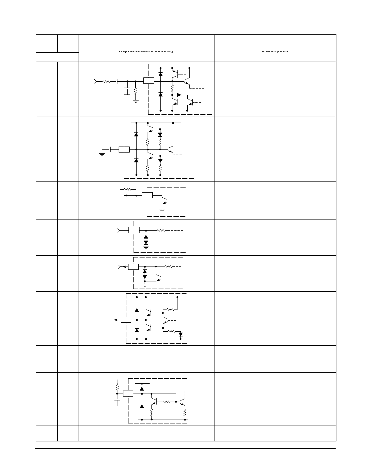
FB FN
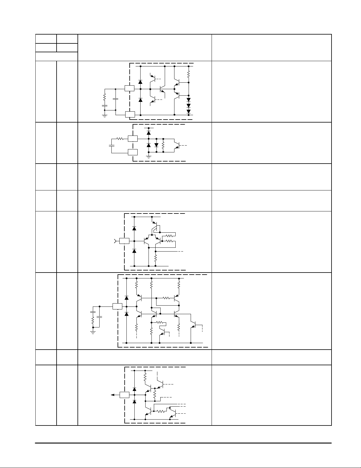
Representative Circuitry
Description
QFP PLCC
Pin
39, 41 1, 3
Video
Input
MC44011
PIN FUNCTION DESCRIPTION
Representative Circuitry Description
(Pin numbers refer to PLCC package)
0.47
470
47 pF
10 M
20 k
(Pin numbers refer to PLCC package)
Video Input 1 & 2 – Video 1 (Pin 1) and Video 2
(Pin 3) are composite video inputs. Either can be
NTSC or PAL. Input impedance is high, termination
must be external. Also used for the luma and chroma
components of an S–VHS signal. Selection of these
inputs is done by software. External components
protect against ESD and noise.
40 2
42 4
43 5
44 6
0.1
5.0
Vertical Sync
From MCU
To/From MCU
2
10 k
ACC Filter – A 0.1 µF capacitor at this pin filters the
feedback loop of the chroma automatic gain control
amplifier. Input chroma burst amplitude can be
between 30 and 600 mVpp.
Vertical Sync Output – An open collector output
4
5
6
100 k
180 k
requiring an external pull–up. Output is an active low
pulse, 500 µs wide, occurring each field. Timing of this
pulse depends on Bit $78–7.
SCL – Clock for the I2C bus interface. See Appendix C
for specifications. Maximum frequency is 100 kHz.
SDL – Bidirectional data line for the I2C bus interface.
As an output, it is an open collector. (Write Address
$8A, Read Address $8B)
1 7
7
(Same as Pin 7)
5.0
9
2 8
3 9
4 10
Field ID
110 k
2.2 µF / /
0.01
(See power distribution diagram at the end of this section.)
MOTOROLA ANALOG IC DEVICE DATA
8.0 k
100 k
20 k
12 k
Field ID – TTL level output indicating Field 1 or Field 2.
Polarity depends on state of Bit $78–7 (Vertical Sync
Delay). See T able 1 1 and Figure 33 and 34.
Burst Gate – TTL level output used for external
clamps, as well as internally. Pulse is active high,
≈ 3.5 µs wide, with the rising edge ≈ 3.0 µs after
center of selected incoming sync pulse.
Reference Current Input – Current supplied to this
pin, typically 32 µA from 5.0 V through a 110 kΩ
resistor, is the reference current for the calibration
circuit. Noise filtering should be done at the pin.
Voltage at this pin is typically 1.2 V.
Quiet Ground – Ground for the horizontal PLL filter
(PLL #1) at Pin 1 1.
9
Page 10
FB FN
QFP
PLCC
Pin
5 11
PIN FUNCTION DESCRIPTION (continued)
Representative Circuitry
Representative Circuitry
(Pin numbers refer to PLCC package)
(Pin numbers refer to PLCC package)
11
100 k
0.1
68 pF
10
MC44011
Description
(Pin numbers refer to PLCC package)
(Pin numbers refer to PLCC package)
H Filter – Components at this pin filter the output of
the phase detector of PLL #1. This PLL becomes
phase–locked to the selected incoming horizontal
sync. External component values are valid for NTSC
and PAL systems.
Description
6 12
7 13
8 14
9 15
10 16
0.047
10 k
470 pF
15 kHz
Return
4700 pF
12 k
12
(Same as Pin 7)
(Same as Pin 7)
15
16
11
Down
1.0 k
6.0 k
6.0 k
1.0 M
10 k
20 k
UpGain
Vert
Gate
H Filter Switch – An internal switch–to–ground which
permits altering the filtering action of the components
at Pin 11.
16 Fh/C
pin provides either a square wave equal to Fh x 16
(≈ 250 kHz), or composite sync, depending on the
setting of Bit $85–6.
Fh Reference – A TTL square wave output which is
phase–locked to the selected incoming horizontal sync.
The rising edge occurs ≈ 1.3 µs after sync center.
15 kHz Return – This TTL input receives the output of
an external frequency divider which is part of PLL #2
(Pixel Clock PLL). This signal will be phase and
frequency–locked to the Fh signal at Pin 14. If PLL #2
is not used, this pin should be connected to a 5.0 V
supply.
PLL #2 Filter – Components at this pin filter the output
of the phase detector of PLL 2. This PLL becomes
phase–locked to the Fh signal at Pin 14.
Recommended values for filter components are
shown. External components should be connected to
ground at Pin 17. If PLL #2 is not used, this pin should
be grounded.
– A TTL level output from PLL #1. This
Sync
11 17
12 18
10
(See power distribution diagram at the end of this section.)
200
Pixel
Clock
Output
18
Gnd3 – Ground for the high frequency PLL #2. Signals
at Pins 15 to 19 should be referenced to this ground.
Pixel Clock Output – Sampling clock output (TTL) for
external A/D converters, and for the external frequency
divider. Frequency range at this pin is 6.0 to 40 MHz.
MOTOROLA ANALOG IC DEVICE DATA
Page 11
FB FN
QFP
PLCC
Pin
13 19
14 20
MC44011
PIN FUNCTION DESCRIPTION (continued)
Representative Circuitry
Representative Circuitry
(Pin numbers refer to PLCC package)
(Pin numbers refer to PLCC package)
(See power distribution diagram at the end of this section.)
20
5.0 V
390
Output
Color
& Gain
Brightness
36 k
Description
(Pin numbers refer to PLCC package)
(Pin numbers refer to PLCC package)
V
– A 5.0 V supply (±5%), for the high frequency
CC3
PLL #2. Decoupling must be provided from this pin to
Pin 17. Ripple on this pin will affect pixel clock jitter.
R/V Output – Red (in RGB mode), or R–Y (in YUV
mode), output from the color difference stage. A
pull–up (390 Ω) to 5.0 V is required. Blank level is
≈ 1.4 Vdc. Maximum amplitude is ≈ 3.0 Vpp,
black–to–white.
Description
15 21
16 22
17 23
18 24
19 25
20, 21,2226, 27,
28
23 29
(Same as Pin 20)
(Same as Pin 20)
(See power distribution diagram at the end of this section.)
(See power distribution diagram at the end of this section.)
25
V
ref
R, G, B
Inputs
100 k
V
ref
Y2
Input
29
100 k
G/Y Output – Green (in RGB mode), or Y (in YUV
mode), output from the color difference stage (same
as Pin 20).
B/U Output – Blue (in RGB mode), or B–Y (in YUV
mode), output from the color difference stage (same
as Pin 20).
V
– A 5.0 V supply (±5%), for the color difference
CC2
stage. Decoupling must be provided from this pin to
Pin 24.
Gnd2 – Ground for the color difference stage. Signals
at Pins 20 to 31 should be referenced to this pin.
FC – Fast Commutate switch. Taking this pin high
(TTL level) connects the RGB inputs (Pins 26 to 28)
to the RGB outputs (Pins 20 to 22), permitting an
overlay function. The switch can be disabled in
software (Bit $80–7).
Blue (26), Green (27), Red (28) Inputs – Inputs to
the color difference stage. Designed to accept
standard analog video levels, these input pins have a
clamp and sync separator. They are selected with
Pin 25 or in software (Bit $80–7).
Y2 Input – Luma #2/Composite sync input. This
luma input to the color difference stage is used in
conjunction with auxiliary color difference inputs,
and/or as a sync input. Clamp and sync separator
are provided.
24, 25 30, 31
R–Y, B–Y
Inputs
26 32
0.47
32
MOTOROLA ANALOG IC DEVICE DATA
B–Y (30), R–Y (31) Inputs – Inputs to the color
V
ref
100 k
difference stage. Designed for standard color
difference levels, these inputs can be capacitor
coupled from the color difference outputs, from a delay
line, or an auxiliary signal source. Input clamp is
provided.
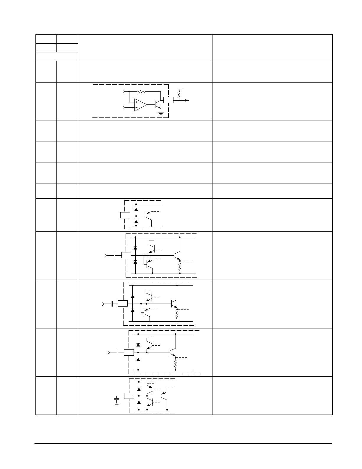
Y1 Clamp – A 0.47 µF capacitor at this pin provides
clamping for the Luma #1 output.
11
Page 12
FB FN
QFP
PLCC
Pin
27 33
MC44011
PIN FUNCTION DESCRIPTION (continued)
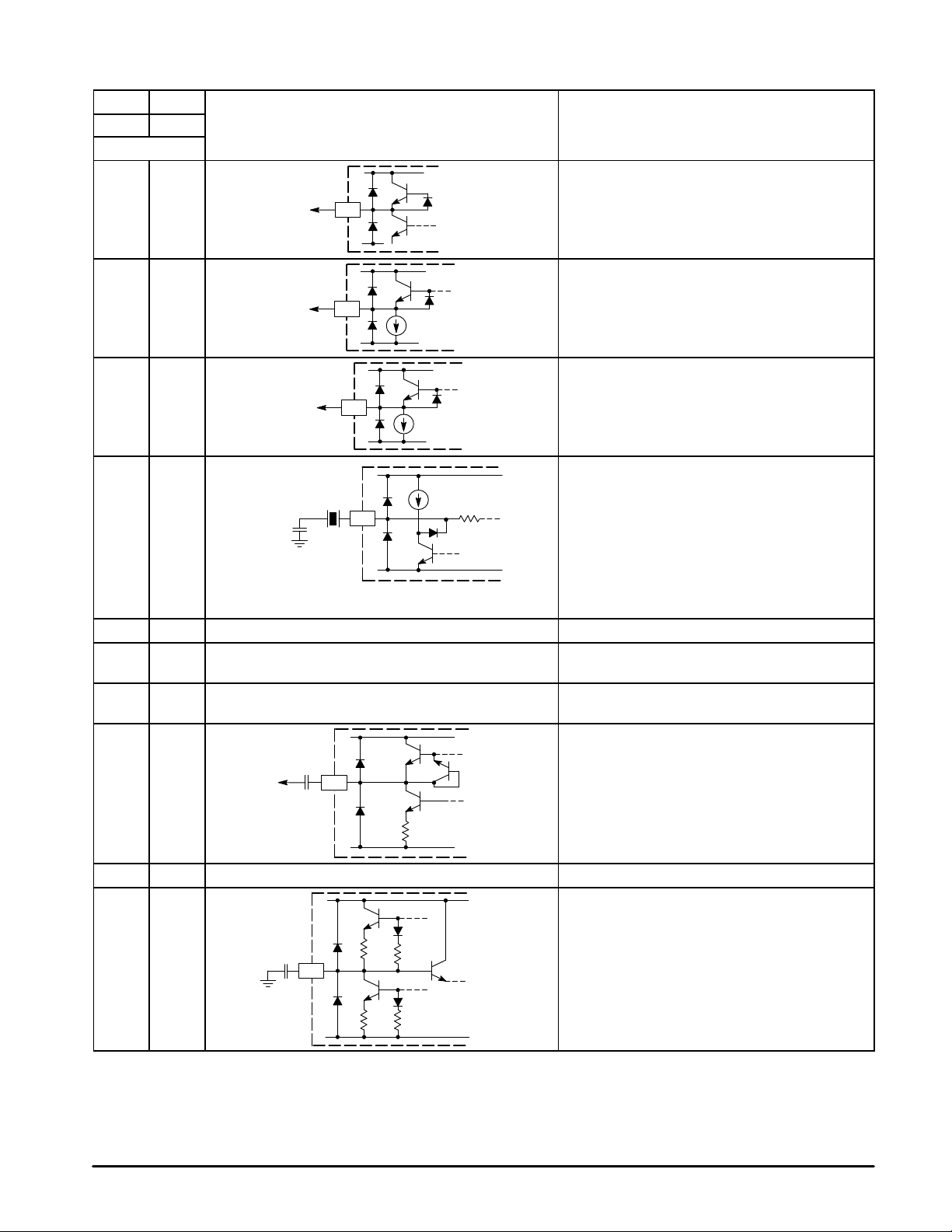
Representative Circuitry
Representative Circuitry
(Pin numbers refer to PLCC package)
(Pin numbers refer to PLCC package)
Y1
Output
33
Description
(Pin numbers refer to PLCC package)
(Pin numbers refer to PLCC package)
Y1 Output – Luma #1 output. This output from the
PAL/NTSC/S–VHS decoder is the luma component of
the decoded composite video at Pin 1 or 3. It is
internally directed to the color difference stage.
Description
28 34
System
Select
29 35
Sandcastle
Pulse
30, 32 36, 38
R = 400 Ω at Pin 38
Ω
R = 300
31 37 No Connect – This pin is to be left open.
33 39
34 40
35 41
(See power distribution diagram at the end of this section.)
(See power distribution diagram at the end of this section.)
at Pin 36
B–Y
34
35
14.3 MHz
17.7 MHz
41
20 µA
R
System Select – A multi–level dc output which
indicates the color decoding system to which the
PAL/NTSC detector is set by the software. This output
is used by the MC44140 chroma delay line.
Sandcastle Pulse – A multi–level timing pulse output
used by the MC44140 chroma delay line. This pulse
encompasses the horizontal sync and burst time.
Xtal 2 (36), Xtal 1 (38) – Designed for connection of 4x
subcarrier color crystals. Selection is done in software.
The selected frequency is used by the PAL/NTSC
detector; system identifier; all notches and traps; delay
lines; and the horizontal calibration circuit.
The crystal frequency should be:
14.3 MHz at Pin 36 for NTSC,
17.7 MHz at Pin 38 for PAL.
(See Table 17 for crystal specifications)
Ground 1 – Ground for all sections except PLL #2
and the color difference stage.
V
– A 5.0 V (±5%), supply to all sections except
CC1
PLL #2 and the color difference stage.
B–Y Output – Output from the PAL/NTSC decoder, it
is typically capacitor–coupled to a delay line or to the
B–Y input. This pin is clamped, and filtered at the
color subcarrier frequency , 2x, and 8x that frequency.
36 42 (Same as Pin 41) R–Y Output – Output from the PAL/NTSC decoder.
37 43
0.1
43
12
Ident Filter – A 0.1 µF capacitor filters the system
identification circuit in the NTSC/PAL decoder.
MOTOROLA ANALOG IC DEVICE DATA
Page 13
FB FN
QFP
PLCC
Pin
38 44
MC44011
PIN FUNCTION DESCRIPTION (continued)
Representative Circuitry
Representative Circuitry
(Pin numbers refer to PLCC package)
(Pin numbers refer to PLCC package)
0.1
47 k
2200 pF
44
Description
(Pin numbers refer to PLCC package)
(Pin numbers refer to PLCC package)
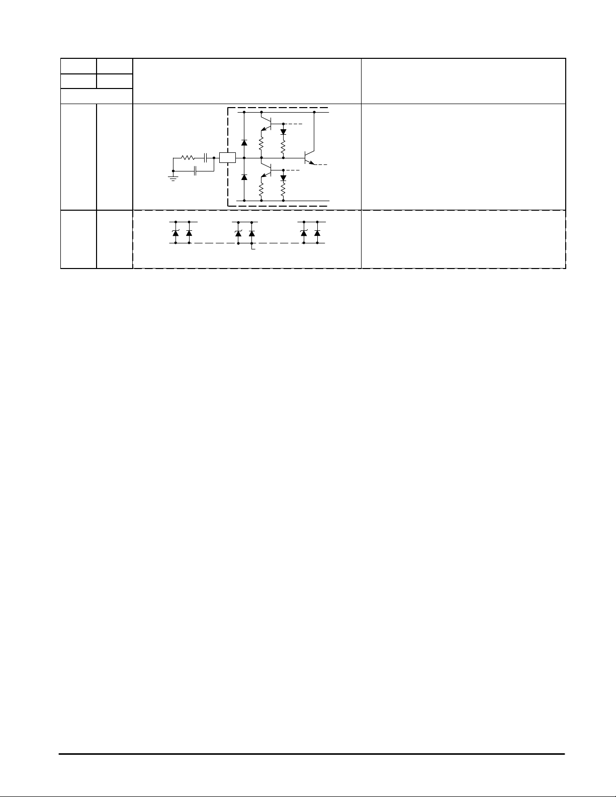
Crystal PLL Filter – Components at this pin filter the
PLL for the crystal chroma oscillator circuit.
Description
4, 11,
13, 17,
18, 33,
34
10, 17,
19, 23,
24, 39,
40
V
CC1
7.0 V
(Dashed lines indicate substrate connection.)
7.0 V
V
CC2
7.0 V
V
CC3
Power Distribution – The three VCC pins must be
externally connected to 5.0 V (±5%) supply. The four
grounds must be externally tied together, preferably to
a ground plane.
MOTOROLA ANALOG IC DEVICE DATA
13
Page 14
10
MC44011
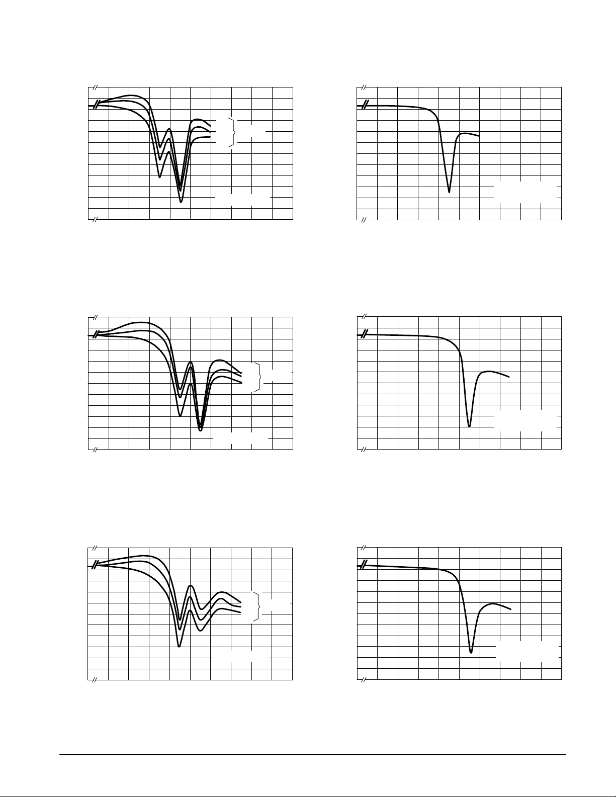
Luma Frequency Response (14.3 MHz) Crystal, (4.5 MHz) Sound Trap
Figure 2. Composite Video Mode Figure 3. S–VHS Mode
10
0
–10
–20
–30
–40
dB GAIN AT Y1 RELATIVE TO VIDEO 1
–50
0.1
10
0
–10
–20
–30
–40
dB GAIN AT Y1 RELATIVE TO VIDEO 1
–50
0.1
0
000
Peaking
010
111
Sound Trap = 1,1
1.0 3.0 5.0 7.0 10
f, FREQUENCY (MHz)
–10
–20
–30
–40
dB GAIN AT Y1 RELATIVE TO VIDEO 1
–50
0.1 1.0 3.0 5.0 7.0 10
f, FREQUENCY (MHz)
Sound Trap = 1,1
All Peaking Settings
Luma Frequency Response (17.7 MHz) Crystal, (5.5 MHz) Sound Trap
Figure 4. Composite Video Mode Figure 5. S–VHS Mode
10
0
000
Peaking
010
111
Sound Trap = 1,1
1.0 3.0 5.0 7.0 10 0.1 1.0 3.0 5.0 7.0 10
f, FREQUENCY (MHz) f, FREQUENCY (MHz)
–10
–20
–30
–40
dB GAIN AT Y1 RELATIVE TO VIDEO 1
–50
Sound Trap = 1,1
All Peaking Settings
10
0
–10
–20
–30
–40
dB GAIN AT Y1 RELATIVE TO VIDEO 1
–50
0.1
14
Luma Frequency Response (17.7 MHz) Crystal, (5.5/5.75 MHz) Sound Trap
Figure 6. Composite Video Mode
000
Peaking
010
111
Sound Trap = 1,1
1.0 3.0 5.0 7.0 10
f, FREQUENCY (MHz)
10
0
–10
–20
–30
Sound Trap = 0,1
–40
dB GAIN AT Y1 RELATIVE TO VIDEO 1
–50
0.1 1.0 3.0 5.0 7.0 10
f, FREQUENCY (MHz)
All Peaking Settings
MOTOROLA ANALOG IC DEVICE DATA
Figure 7. S–VHS Mode
Page 15
MC44011
Luma Frequency Response (17.7 MHz) Crystal, (6.0 MHz) Sound Trap
Figure 8. Composite Video Mode
10
0
–10
000
Peaking
–20
010
111
–30
–40
dB GAIN AT Y1 RELATIVE TO VIDEO 1
–50
0.1 1.0 3.0 5.0 7.0 10 0.1 1.0 3.0 5.0 7.0 10
Sound Trap = 1,0
10
0
–10
–20
–30
–40
dB GAIN AT Y1 RELATIVE TO VIDEO 1
–50
Figure 9. S–VHS Mode
Sound Trap = 1,0
All Peaking Settings
f, FREQUENCY (MHz)f, FREQUENCY (MHz)
Luma Frequency Response (17.7 MHz) Crystal, (6.5 MHz) Sound Trap
Figure 10. Composite Video Mode Figure 11. S–VHS Mode
10
–10
–20
–30
0
000
Peaking
010
111
10
0
–10
–20
–30
–40
dB GAIN AT Y1 RELATIVE TO VIDEO 1
–50
0.1
–10
–15
–20
–25
–30
–35
dB GAIN AT Y1 RELATIVE TO VIDEO 1
–40
3.0
Sound Trap = 0,0
All Peaking Settings
Sound Trap = 0,0
–40
dB GAIN AT Y1 RELATIVE TO VIDEO 1
–50
1.0 3.0 5.0 7.0 10 1.0 3.0 5.0 7.0 10
0.1
f, FREQUENCY (MHz) f, FREQUENCY (MHz)
Figure 12. (3.58 MHz) Chroma Notch Figure 13. (4.43 MHz) Chroma Notch
–10
Gain at
Peaking =
000
001
100
101
010
011
110
111
Sound Trap = 1,1
14.3 MHz Crystal
–15
–20
–25
Gain at
Peaking =
–30
–35
dB GAIN AT Y1 RELATIVE TO VIDEO 1
3.5 4.0 4.5 5.0
–40
4.0
000
001
100
101
010
011
110
111
f, FREQUENCY (MHz)f, FREQUENCY (MHz)
Sound Trap = 1,1
17.7 MHz Crystal
MOTOROLA ANALOG IC DEVICE DATA
15
Page 16
–15
MC44011
(4.5 MHz) Sound Trap
Figure 14. Composite Video Mode Figure 15. S–VHS Mode
–10
–20
–25
–30
–35
–40
dB GAIN AT Y1 RELATIVE TO VIDEO 1
–45
4.0
–15
–20
–25
–30
–35
–40
dB GAIN AT Y1 RELATIVE TO VIDEO 1
–45
5.0
–15
–20
–25
–30
Sound Trap = 1,1
Peaking = 111
14.3 MHz Crystal
dB GAIN AT Y1 RELATIVE TO VIDEO 1
4.5 5.0 4.0 4.5 5.0
Sound Trap = 1,1
–35
Peaking = 111
14.3 MHz Crystal
–40
f, FREQUENCY (MHz)f, FREQUENCY (MHz)
(5.5 MHz) Sound Trap
Figure 16. Composite Video Mode Figure 17. S–VHS Mode
–5.0
–10
–15
–20
–25
–30
–35
Sound Trap = 1,1
Peaking = 111
17.7 MHz Crystal
dB GAIN AT Y1 RELATIVE TO VIDEO 1
5.5 6.0 5.5 6.0
f, FREQUENCY (MHz) f, FREQUENCY (MHz)
Sound Trap = 1,1
Peaking = 111
–40
17.7 MHz Crystal
–45
5.0
–10
–15
–20
–25
–30
–35
dB GAIN AT Y1 RELATIVE TO VIDEO 1
–40
5.0
16
(5.5 + 5.75 MHz) Sound Trap
Figure 18. Composite Video Mode
Sound Trap = 0,1
Peaking = 111
17.7 MHz Crystal
5.4 6.6 5.4 6.65.8 6.25.8 6.2
–5.0
–10
–15
–20
–25
–30
–35
–40
dB GAIN AT Y1 RELATIVE TO VIDEO 1
–45
5.0
Figure 19. S–VHS Mode
Sound Trap = 0,1
Peaking = 111
17.7 MHz Crystal
f, FREQUENCY (MHz)f, FREQUENCY (MHz)
MOTOROLA ANALOG IC DEVICE DATA
Page 17

MC44011
(6.0 MHz) Sound Trap
–10
–15
–20
–25
–30
–35
dB GAIN AT Y1 RELATIVE TO VIDEO 1
–40
5.5
–15
–20
Figure 20. Composite Video Mode
Sound Trap = 1,0
Peaking = 111
17.7 MHz Crystal
6.0 6.5 5.5 6.0 6.5
Figure 22. Composite Video Mode
–5.0
–10
–15
–20
–25
–30
–35
–40
–45
(6.5 MHz) Sound Trap
–15
–20
Figure 21. S–VHS Mode
Sound Trap = 1,0
Peaking = 111
17.7 MHz Crystal
f, FREQUENCY (MHz)f, FREQUENCY (MHz)
Figure 23. S–VHS Mode
–25
–30
–35
–40
dB GAIN AT Y1 RELATIVE TO VIDEO 1
–45
6.0
–25
–30
–35
Sound Trap = 0,0
Peaking = 111
17.7 MHz Crystal
6.5 7.0 6.5 7.0
f, FREQUENCY (MHz) f, FREQUENCY (MHz)
–40
dB GAIN AT Y1 RELATIVE TO VIDEO 1 dB GAIN AT Y1 RELATIVE TO VIDEO 1
–45
6.0
Figure 24. FC Input Current
0
–20
A)
µ
(
–40
–60
INPUT CURRENT
,l
in
–80
VCC = 5.0 V
Sound Trap = 0,0
Peaking = 111
17.7 MHz Crystal
–100
0
MOTOROLA ANALOG IC DEVICE DATA
1.0 4.02.0 3.0
PIN 25 VOLTAGE (V)
5.0
17
Page 18

Video Input
(@ Pins 1 or 3)
MC44011
Figure 25. Horizontal PLL1 Timing/Composite Video Inputs
C
L
Burst Gate
(Pin 8)
Fh Ref
(Pin 14)
16Fh Out
(Pin 13)
Comp Sync Out
(Pin 13)
Sandcastle Out
(Pin 35)
1.3
µ
2.6
3.1 µs
s
0.7
3.3 µs
µ
s
3.5 µs
4.5 V
1/2Fh
1.3
µ
s
µ
s
(1.4 µs during vertical interval)
4.0 V
3.0 V
5.0 µs5.9 µs
4.5 V
4.5 V
1/16Fh
4.5 V
1.55 V
0 V
18
NOTE: In above waveforms, all timing is referenced to the center of the incoming Sync Pulse at Pin 1 or 3.
Above timings based on a 4.6
Lower two levels of Sandcastle output alternate, based on video system in effect.
All timings are nominal, and apply to both PAL and NTSC signals.
µs wide sync pulse.
Figure 26. Horizontal PLL1 Noise Gate and Filter Pin
Video Input
(@ Pins 1 or 3)
Noise Gate
Charge Pump Current
(Pin 11)
Voltage Waveform
(Pin 11)
16 µs
700 mVpp with High Gain
250 mVpp with Low Gain
MOTOROLA ANALOG IC DEVICE DATA
Page 19

Video Input
(@ Pins 26 to 29)
MC44011
Figure 27. Horizontal PLL1 Timing/R, G, B and Y2 Inputs
C
L
Burst Gate
(Pin 8)
Fh Ref
(Pin 14)
16Fh Out
(Pin 13)
Comp Sync Out
(Pin 13)
Sandcastle Out
(Pin 35)
650 ns
3.3 µs
5.9 µs
2.5
µ
2.0
4.7 µs
3.5 µs
s
µ
s
1.3
µ
s
(1.4 µs during vertical interval)
4.0 V
5.0 µs
4.5 V
4.5 V
1/2Fh
4.5 V
1/16Fh
4.5 V
3.0 V
1.55 V
0 V
R, G, B Outputs
(@ Pins 20 to 22)
NOTE: In above waveforms, all timing is referenced to the center of the incoming Sync Pulse at Pin 26 to 28, or 29.
Above timings based on a 4.6
Lower two levels of Sandcastle output alternate, based on video system in effect.
C
L
70 ns
MOTOROLA ANALOG IC DEVICE DATA
µs wide sync pulse.
19
Page 20

Video Input
(@ Pins 1 or 3)
R–Y, B–Y Outputs
(@ Pins 41, 42)
MC44011
Figure 28. System Timing/Video Inputs to RGB Outputs
50%
700 ns
50%
850 ns
50%
R, G, B Outputs
(@ Pins 20 to 22)
Input @ Pin 25
R, G, B Outputs
(@ Pins 20 to 22)
50 ns
Color Difference
Inputs Enabled
Figure 29. Fast Commutate Timing
0.5 V
50%
RGB Inputs
Enabled
0.5 V
90 ns
50%
Color Difference
Inputs Enabled
20
MOTOROLA ANALOG IC DEVICE DATA
Page 21

Composite Input
(@ Pins 1, 3, 26 to 29)
Fh Ref
(Pin 14)
Burst Gate
(Pin 8)
Composite Sync
(Pin 13)
MC44011
Figure 30. Horizontal Outputs versus Fields (NTSC System)
Line 1
Field 1Field 2
Composite Input
(@ Pins 1, 3, 26 to 29)
Fh Ref
(Pin 14)
Burst Gate
(Pin 8)
Composite Sync
(Pin 13)
Field 2Field 1
MOTOROLA ANALOG IC DEVICE DATA
21
Page 22

Composite Input
(@ Pins 1, 3, 26 to 29)
Fh Ref
(Pin 14)
Burst Gate
(Pin 8)
Composite Sync
(Pin 13)
MC44011
Figure 31. Horizontal Outputs versus Fields (PAL System)
Line 1
Field 1/3Field 2/4
Composite Input
(@ Pins 1, 3, 26 to 29)
Fh Ref
(Pin 14)
Burst Gate
(Pin 8)
Composite Sync
(Pin 13)
Fh Ref
(Pin 14)
Field 2/4Field 1/3
Figure 32. Horizontal PLL2 Timing
60 ns
22
15 kHz Return
(Pin 15)
Determined by
External Circuit
(Must be > 200 ns)
MOTOROLA ANALOG IC DEVICE DATA
Page 23

MC44011
Figure 33. Vertical T iming (NTSC System)
A) Bit $78–7 = 0
Video Input
Vert Sync Out
(Pin 4)
Field Ident Out
(Pin 7)
Video Input
Vert Sync Out
(Pin 4)
Field Ident Out
(Pin 7)
B) Bit $78–7 = 1
Line 1
Line 1
36
µ
s
Field 1Field 2
110 µs
µ
s
36
Field 2Field 1
68 µs
500 µs
500 µs
Video Input
Vert Sync Out
(Pin 4)
Field Ident Out
(Pin 7)
Video Input
Vert Sync Out
(Pin 4)
Field Ident Out
(Pin 7)
µ
s
68
Field 1Field 2
100
µ
s
µ
s
68
Field 2Field 1
144 µs
500 µs
500 µs
MOTOROLA ANALOG IC DEVICE DATA
23
Page 24

MC44011
Figure 34. Vertical T iming (PAL System)
A) Bit $78–7 = 0
Video Input
Vert Sync Out
(Pin 4)
Field Ident Out
(Pin 7)
Video Input
Vert Sync Out
(Pin 4)
Field Ident Out
(Pin 7)
Line 1
36
36 µs
Field 1/3Field 2/4
Field 2/4Field 1/3
68 µs
µ
s
110 µs
500 µs
500 µs
B) Bit $78–7 = 1
Video Input
Vert Sync Out
(Pin 4)
Field Ident Out
(Pin 7)
Video Input
Vert Sync Out
(Pin 4)
Field Ident Out
(Pin 7)
Line 1
Field 1/3Field 2/4
Field 2/4Field 1/3
µ
68
100 µs
68
µ
144 µs
s
500 µs
s
500 µs
24
MOTOROLA ANALOG IC DEVICE DATA
Page 25

MC44011
FUNCTIONAL DESCRIPTION
Introduction
The MC44011, a member of the MC44000 Chroma 4
family , is a composite video decoder which has been tailored
for applications involving multimedia, picture–in–picture, and
frame storage (although not limited to those applications).
The first stage of the MC44011 provides color difference
signals (R–Y, B–Y, and Y) from one of two (selectable)
composite video inputs, which are designed to receive PAL,
NTSC, and S–VHS (Y,C) signals. The second stage provides
either RGB or YUV outputs from the first stage’s signals, or
from a separate (internally selectable) set of RGB inputs,
permitting an overlay function to be performed. Adjustments
can be made to saturation; hue; brightness; contrast;
brightness balance; contrast balance; U and V bias;
subcarrier phase; and color difference gain ratio.
The above mentioned video decoding sections provide the
necessary luma/delay function, as well as all necessary
filters for sound traps, luma/chroma separation, luma
peaking, and subcarrier rejection. External tank circuits and
luma delay lines are not needed. For PAL applications, the
MC44140 chroma delay line provides the necessary
line–by–line corrections to the color difference signals
required by that system.
The MC44011 provides a pixel clock to set the sampling
rate of external A/D converters. This pixel clock, and other
horizontal frequency related output signals, are
phase–locked to the incoming sync. The VCO’s gain is
adjustable for optimum performance. The MC44011 also
provides vertical sync and field identification (Field 1, Field 2)
outputs.
Selection of the various inputs, outputs, and functions, as
well as the adjustments, is done by means of a two–wire I2C
interface. The basic procedure requires the microprocessor
system to read the internal flags of the MC44011, and then
set the internal registers appropriately. This I2C interface
eliminates the need for manual controls (potentiometers) and
external switches. All of the external components for the
MC44011, except for the two crystals, are standard value
resistors and capacitors, and can be non–precision.
(The DACs mentioned in the following description are 6–bits wide. The
settings mentioned for them are given in decimal values of 00 to 63.
These are not hex values.)
P AL/NTSC/S–VHS Decoder
A block diagram of this decoder section is shown in
Figure 35. This section’s function is to take the incoming
composite video (at Pins 1 or 3), separate it into luma and
chroma information, determine if the signal is PAL or NTSC
(for the flags), and then provide color difference and luma
signals at the outputs. If the input is S–VHS, the luma/chroma
separation is bypassed, but the other functions are still
in effect.
Comp
Video 1
Comp
Video 2
ACC Filter
Chroma PLL Filter
Xtal 1
Xtal 2
Figure 35. PAL/NTSC/S–VHS Decoder Block Diagram
Select
($88–7)
1
3
To
Sync
Sep
2
44
38
36
Switches shown with control bits = 0.
4.4/4.8/5.2
5.5/6.0/6.5 MHz
($7B–7,6)
($77–6)
PLL
Oscillator
Sound
Trap
Phase Adjust ($79–5/0)
C
Chroma
Filter
Crystal Select
($7A–7)
Chroma Trap and
Luma Peaking
($7D–7; $7E–7,6)
Flag 23
C
(ACC Active)
ACC
($77–7)
295/244 ns
Luma
Delay
Flag 24
(PAL)
PAL/NTSC
Decoder
Saturation ($87–5/0)
Hue ($88–5/0)
Color Balance ($78–5/0)
Color System
($7C–7,6; $7D–6)
Blanking
To Color
Diff Stage
Adjustable
Luma Delay
($7F–7,6; $80–6)
Ident
Circuit
3.6/7.2/28.6/4.4/
8.8/35.4 MHz Notch
C
3.6/7.2/28.6/4.4/
8.8/35.4 MHz Notch
33
32
34
43
42
41
Y1 Out
Y1 Clamp
System
Select
Ident
Filter
R–Y Out
B–Y Out
MOTOROLA ANALOG IC DEVICE DATA
25
Page 26

MC44011
17.73 MHZ
14.32 MHz
Inputs
The inputs at Pins 1 and 3 are high impedance inputs
designed to accept standard 1.0 Vpp positive video signals
(with negative going sync). The inputs are to be
capacitor–coupled so as not to upset the internal dc bias.
When normal composite video is applied, the desired input is
selected by Bit $88–7. Bits $77–6 and $77–7 must be set to
0 so that their switches are as shown in Figure 35. The
selected signal passes through the sound trap, and is then
separated by the chroma trap and the chroma (high
pass) filter.
When S–VHS signals (Y,C) are applied to the two inputs,
Bit $88–7 is used to direct the luma information to the sound
trap, and the chroma information to the ACC circuit
(Bit $77–6 must be set to a Logic 1). Bit $77–7 is normally
set to a Logic 1 in this mode to bypass the first luma delay
line and the chroma trap, but it can be left 0 if the additional
delay is desired.
Sound Trap
The sound trap will filter out any residual sound subcarrier
at the frequency selected by control bits T1 and T2 according
to Table 3. The accuracy of the notch frequency is directly
related to the selected crystal frequency.
T able 3. Sound Trap Frequency
Crystal
Frequency
T1
($7B–7)T1($7B–6)
0 0 6.5 MHz
0 1 5.5 + 5.75 MHz
1 0 6.0 MHz
1 1 5.5 MHz
0 0 5.25 MHz
0 1 4.44 + 4.64 MHz
1 0 4.84 MHz
1 1 4.44 MHz
Notch
Frequency
Code 01 (for T1, T2) is used to widen the band rejection
where stereo is in use. Typical rejection is 30 dB.
ACC and PAL/NTSC Decoder
The chroma filter bandpass characteristics (3.58 or
4.43 MHz) is determined by the selected crystal. The output
of the chroma filter is sent to the ACC circuit which detects
the burst signal, and provides automatic gain control once
the crystal oscillator has achieved phase lock–up to the
burst. The dc voltage at Pin 2 is ≈ 1.5 to 2.0 V . This will occur
if the burst amplitude exceeds 30 mVpp, and if the correct
crystal is selected (Bit $7A–7). A 17.734472 MHz crystal is
required for PAL, and a 14.31818 MHz crystal is required for
NTSC. When Flag 23 is high, it indicates that the crystal’s
PLL has locked up, and the ACC circuit is active, providing
automatic gain control. A small amount of phase adjustment
(≈±5°) of the crystal PLL, for color correction, can be made
with control DAC $79–5/0. Pin 2 is the filter for the ACC loop,
and Pin 44 is the filter for the crystal oscillator PLL.
The PAL/NTSC decoder then determines if the signal is
PAL or NTSC by looking for the alternating phase
characteristic of the PAL burst. When Flag 24 is high, PAL
has been detected. Bits SSA, SSB, SSC, and SSD (Table 4)
must then be sent to the decoder to set the appropriate
decoding method.
T able 4. Color System Select
SSA
($7C–6)
0 0 0 0 Not Used
0 1 0 0 PAL
1 0 0 0 NTSC
1 1 0 0 Color Kill
X X 1 0 External
SSB
($7D–6)
SSC
($7C–7)
SSD
($7A–6)
Color
System
Upon receiving the SSA to SSD bits, the decoder provides
the correct color difference signals, and with the Identification
circuit, provides the correct level at the System Select output
(Pin 34). This output is used by the MC44140 delay line.
The color kill setting (SSA = SSB = 1) should be used
when the ACC flag is 0, when the color system cannot be
properly determined, or when it is desired to have a
black–and–white output (the ACC circuit and flag will still
function if the input signal has a burst signal). The “External”
setting (SSC = 1) is used when an external (alternate) source
of color difference signals are applied to the MC44140 delay
line. (See Miscellaneous Applications Information for more
details.)
Color Difference Controls and Outputs
The color difference signals (R–Y, B–Y) from the
PAL/NTSC decoder are directed to the saturation, hue and
color balance controls, and then through a series of notch
filters before being output at Pins 41 and 42. Blanking and
clamping are applied to these outputs.
The saturation control DAC($87–5/0) varies the amplitude
of the two signals from 0 Vpp (DAC setting = 00), to a
maximum of ≈ 1.8 Vpp (at a DAC setting of 63). The
maximum amplitude (without clipping) is ≈ 1.5 Vpp, but a
nominal setting is ≈ 1.3 Vpp at a DAC setting of 15.
The hue control ($88–5/0) varies the relative amplitude of
the two signals to provide a hue adjustment. The nominal
setting for this DAC is 32.
The color balance control ($78–5/0) provides a fine
adjustment of the relative amplitude of the two outputs. This
provides for a more accurate color setting, particularly when
NTSC signals are decoded. The nominal setting for this DAC
is 32, and should be adjusted before the hue control is
adjusted.
The notch filters provide filtering at the color burst
frequency, and at 2x and 8x that frequency. Additionally,
blanking and clamping (derived from the horizontal PLL) are
applied to the signals at this stage. The nominal output dc
level is ≈ 2.0 to 2.5 Vdc, and the load applied to these outputs
should be >10 kΩ. Sync is not present on these outputs.
26
MOTOROLA ANALOG IC DEVICE DATA
Page 27

MC44011
Luma Peaking, Delay Line, and Y1 Output
When composite video is applied, the luma information
extracted in the chroma trap is then applied to a stage which
allows peaking at ≈ 3.0 MHz with the 17.7 MHz crystal
(≈ 2.2 MHz with the 14.3 MHz crystal). The amount of
peaking at Y1 is with respect to the gain at the minimum
peaking value (P1, P2, P3 = 111), and is adjustable with
Bits $7D–7, and $7E–7,6 according to Table 5.
The luma delay lines allow for adjustment of that delay so
as to correspond to the chroma delay through this section.
Table 6 indicates the amount of delay using the D1–D3 bits
($7F–7,6, and $80–6). The delay indicated is the total delay
from Pin 1 or 3 to the Y1 output at Pin 33. The amount of
delay depends on whether Composite Video is applied, or YC
signals (S–VHS) are applied.
The output impedance at Y1 is ≈ 300 Ω, and the black level
P1
($7D–7)P2($7E–6)P3($7E–7)
0 0 0 9.5 dB
0 0 1 8.5
1 0 0 7.7
1 0 1 6.5
0 1 0 5.3
0 1 1 3.8
1 1 0 2.2
1 1 1 0
17.7 MHz Crystal, 6.5 MHz Sound Trap, Composite V ideo Mode
T able 5. Luma Peaking
clamp is at ≈ 1.1 V. Sync is present on this output. Y1 is also
internally routed to the color difference stage.
T able 6. Luma Delay
14.3 MHz Crystal 17.7 MHz Crystal
D1
($7F–6)D2($80–6)
0 0 0 690 ns 395 ns 594 ns 350 ns
0 0 1 760 465 650 406
0 1 0 830 535 707 463
0 1 1 900 605 763 519
1 0 0 970 675 819 575
1 0 1 1040 745 876 632
1 1 0 970 675 819 575
1 1 1 1040 745 876 632
D3
($7F–7)
Comp. Video
($77–7 = 0)
S–VHS
($77–7 = 1)
Composite Video
($77–7 = 0)
Y1
Peaking
S–VHS
($77–7 = 1)
Color Difference Stage and RGB/YUV Outputs
A block diagram of this section is shown in Figure 36. This
section’s function is to take the color difference input signals
(Pins 30, 31), or the RGB inputs (Pins 26 to 28), and output
the information at Pins 20 to 22 as either RGB or YUV.
The inputs (on the left side of Figure 36) are analog RGB,
or color difference signals (R–Y and B–Y) with Y1 or Y2 as
the luma component. Pin 25 (Fast Commutate) is a logic level
T able 7. Color Difference Input/Output Selection
RGB EN
FC
1 0 0 0 RGB inputs, RGB outputs, no saturation control
1 0 1 0 RGB inputs, RGB outputs, with saturation control
1 0 1 1 RGB inputs, YUV outputs, with saturation control
1 0 0 1 Not usable
FC Low and/or
RGB EN
FC Low and/or
RGB EN Hi
$80–7
Hi
YX EN
$82–6
X 0 R–Y, B–Y inputs, RGB outputs. Y1 or Y2 must be selected
X 1 R–Y, B–Y inputs, YUV outputs. Y1 or Y2 must be selected
YUV EN
$82–7
input, used in conjunction with RGB EN
(Bit $80–7), to select
the RGB inputs or the color difference inputs. The outputs
(Pins 20 to 22) are either RGB or YUV, selected with
Bit $82–7. The bit numbers adjacent to the various switches
and gates indicate the bits used to control those functions.
Table 7 indicates the modes of operation.
Function
MOTOROLA ANALOG IC DEVICE DATA
27
Page 28

MC44011
In addition to Table 7, the following guidelines apply:
a. To select the RGB inputs, both FC must be high and
RGB EN
must be low. Therefore, the RGB inputs can
be selected either by the I2C bus by leaving FC
permanently high, or by the FC input by leaving
Bit $80–7 permanently low. For overlay functions,
where high speed, well controlled switching is
necessary, the FC pin must be the controlling input.
b. When the R–Y, B–Y inputs are selected, either Y1 or Y2
must be selected, and the other must be deselected.
The YX input is automatically disabled in this mode.
c. In applications where the color difference inputs are
obtained from the NTSC/PAL decoder (from a
composite video signal), Y1 is used. The Y2 input is
normally used where alternately sourced color
difference signals are applied, either through the
MC44140 delay line, or through other external switching
to Pins 30 and 31.
In Figure 36, the bit numbers followed by “–0/5” indicate
DAC operated controls (contrast, brightness, etc.), which are
controlled by the I2C bus. The DACs have 6–bit resolution,
allowing 64 adjustment steps. Table 8 provides guidelines on
the DAC operation.
Table 8. DAC Operation – Color Difference Section
Function Bits RGB Outputs ($82–7 = 0) YUV Outputs ($82–7 = 1)
Brightness $84–0/5 Affects dc black and maximum levels of the three
∆ DC – Red
∆ DC – Blue
Contrast $81–0/5 Provides gain adjustment (black–to–white) of the
∆ Gain – Red
∆ Gain – Blue
V DC
U DC
Main Saturation $86–0/5 Affects color saturation, except when the RGB
$85–0/5
$83–0/5
$82–0/5
$80–0/5
$7E–0/5
$7D–0/5
outputs, but not the clamp level, nor the amplitude.
Fine tune the Red and Blue brightness levels. Allows a small amount of color tint control (not to
three outputs.
Fine tune the Red and Blue contrast levels. Fine tune of the U and V gain levels.
Must be set to 00. Should nominally be set to 32. This sets the dc
inputs bypass this section (YX EN = 0).
Affects dc black and white levels of the Y output
only, but not the clamp level, nor the amplitude.
be confused with hue).
Provides gain adjustment of the three outputs.
level of the U and V outputs at ≈ mid–scale.
Affects color saturation levels of the UV outputs.
Does not affect the Y output.
Inputs
R
G
B
R–Y
B–Y
Y2
F/C
C
28
C
27
26
C
31
C
C
30
29
C
(From Decoder)
25
YX
$81–7
$81–6
Y1
$80–7
Matrix
Decoder
$82–6
Figure 36. Color Difference Stage and Outputs
Contrast
$81–0/5
$82–0/5
Main Saturation
$86–0/5
R–YB–YYX
R–Y
G–Y
B–Y
Y
R
G
B
$82–7
NOTES:
Brightness
$84–0/5
$82–7
∆
∆
Gain
∆
($80–0/5)
1. = Clamp Circuit
C
2. Switches controlled by
I2C Interface – See Text.
DC ($85–0/5)
V DC ($7E–0/5)
∆
DC ($83–0/5)
Gain
U DC ($7D–0/5)
20
21
22
5.0
R/V
5.0
G/Y
5.0
B/U
390
390
390
Ω
Ω
Outputs
Ω
28
MOTOROLA ANALOG IC DEVICE DATA
Page 29

MC44011
The RGB and Y2 inputs are designed to accept standard
1.0 Vpp analog video signals. They are not designed for TTL
level signals. The color difference inputs are designed to
accept signals ranging up to 1.8 Vpp. All signals are to be
capacitor–coupled as clamping is provided internally. Input
impedance at these six pins is high.
For applications involving externally supplied color
difference signals, sync can be supplied on the luma input
(Y2), or it can be supplied separately at the RGB inputs.
Where the color difference signals are obtained from the
NTSC/PAL decoder, sync is provided to this section on the
internal Y1 signal. See Sync Separator section for more
details on injecting sync into the MC4401 1.
Sync is present on all three outputs in the RGB mode, and
on the Y output only (Pin 21) in the YUV mode.
The Fast Commutate input (FC, Pin 25) is a logic level
input with a threshold at ≈ 0.5 V. Input impedance is ≈ 67 kΩ,
and the graph of Figure 24 shows the input current
requirements. Propagation delay from the FC pin to the
RGB/YUV outputs is ≈ 50 ns when enabling the RGB inputs,
and ≈ 90 ns when disabling the inputs. (See Figure 29 Fast
Commutate Timing diagram.) If Pin 25 is open, that is
equivalent to a Logic 1, although good design practices
dictate that inputs should never be left open. The voltage on
this pin should not be allowed to go more than 0.5 V above
V
or below ground.
CC2
The three outputs (Pins 20 to 22) are open–collector,
requiring an external pull–up. A representative schematic is
shown in Figure 37.
The output amplitude can be varied from 100 mVpp to
3.0 Vpp by use of the contrast and saturation controls. Any
output load to ground should be kept larger than 1.0 kΩ. In
the RGB mode, DACs $7D and $7E should be set to 00,
which results in clamping levels of ≈ 1.4 Vdc. In the YUV
mode, DACs $7D and $7E should be set to 00, which results
Figure 37. Output Stage
∆
DC
5.0
36 k
5.0
390
Output
Color or
Color Diff
Contrast
∆
Gain
Brightness
in clamping levels of ≈ 1.4 Vdc. In the YUV mode, the DACs
should be set to 32 to bias the U and V outputs to ≈ 2.3 V. The
Y output clamp will remain at ≈ 1.4 V in the YUV mode.
Horizontal PLL (PLL1)
PLL1 (shown in Figure 38) provides several outputs which
are phase–locked to the incoming horizontal sync. In normal
operation, the two switches at the left side of Figure 38 are as
shown, and (usually) the transistor at Pin 12 is off.
The phase detector compares the incoming sync (from the
sync separator) to the frequency from the ÷ 64 block. The
phase detector’s output, filtered at Pin 11, controls the VCO
to set the correct frequency (≈ 1.0 MHz) so that the output of
the ÷ 64 is equal to the incoming horizontal frequency.
The line–locked outputs are:
1) Fh Ref (Pin 14) – A square wave, TTL levels, at the
horizontal frequency, and phase–locked to the sync
source according to the timing diagram of Figures 25
and 27.
2) Burst Gate (Pin 8) – This is a positive going pulse, TTL
levels, coincident with the burst signal. See the timing
diagram of Figures 25 and 27.
Frequency
Divider
4.43 MHz/
3.58 MHz
SC
$78–6
525/625
($84–6)
$86–6
Frequency
Comparator
Up/Down
Converter
VCO
From Sync
Separator
Figure 38. Horizontal PLL (PLL1)
Calibration Loop
Counter
D–to–A
1.0 MHz
16Fh
13 11
16Fh/
C
Sync
Divide By 64
$85–6
Frame
I
ref
Burst
Gate
358
S/C
OutFhRef
f
H
Horiz Sync
14
from Sync
Separator
Phase
Det 1
H Filter
To PLL #2
Flag 12
(Horizontal not locked)
Coincidence
Detector
L1 Gain
$83–6
Gate
$77–2
$84–7
12
H Filter
Switch
MOTOROLA ANALOG IC DEVICE DATA
29
Page 30

MC44011
3) Sandcastle Output (Pin 35) – This is a multilevel
output, at the horizontal frequency, used by the
MC44140 delay line. See the timing diagram of
Figures 25 and 27.
4) 16Fh/C
TTL levels, user selectable. When Bit $85–6 is set to 0,
Pin 13 is a square wave at 16x the horizontal frequency
(250 kHz for PAL, ≈ 252 kHz for NTSC). When Bit $85–6
is set to 1, Pin 13 is negative composite sync, derived
from the internal sync separator. See the timing diagram
of Figures 25 and 27.
The first three outputs mentioned above, and Pin 13 when
set to 16Fh, are consistent, and do not change duty cycle or
wave shape during the vertical sync interval. These four
outputs will also be present regardless of the presence of a
video signal at the selected input.
When Pin 13 is set to C
composite sync format. If there is no video signal present at
the selected input, this output will be a steady logic high.
Loading on these pins should not be less than 2.0 kΩ to
either ground or 5.0 V.
Pin 11 is the filter for the PLL, and requires the
components shown in Figure 38, and with the values shown
in the application circuit of Figure 42. Pin 12 is a switch which
allows the filtering characteristics at Pin 11 to be changed.
Switching in the additional components (set $84–7 = 1)
increases the filter time constant, permitting better
performance in the presence of noisy signals.
The gain of the phase detector may be set high or low,
depending on the jitter content of the incoming horizontal
frequency, by using Bit $83–6. Broadcast signals usually
have a very stable horizontal frequency, in which case the
low gain setting ($83–6 = 0) should be used. When the video
source is, for example, a VCR, the high gain setting may be
preferable to minimize instability artifacts which may show up
on the screen.
The gating function ($77–2) provides additional control
where the stability of the incoming horizontal frequency is in
question. With this bit set to 0, gating is in effect, causing the
phase detector to not respond to the incoming sync pulses
during the vertical interval. This reduces disturbances in this
PLL due to the half–line pulses and their change in polarity.
The gating may be disabled by setting this bit to 1 where the
timing of the incoming sync is known to be stable. The gating
cannot be enabled if the phase detector gain is set high
($83–6 = 1).
Calibration Loop
The calibration loop (upper left portion of Figure 38)
maintains a near correct frequency of this PLL in the absence
of incoming sync signals. This feature minimizes
re–adjustment and lock time when sync signals are
re–applied. The calibration loop is similar to the PLL function,
receiving one frequency from the crystal (either 4.43 MHz or
3.58 MHz) divided down to a frequency similar to the
standard horizontal frequency. Bit $84–6 is used to set the
frequency divider to the correct ratio, depending on which
crystal is selected (see Table 9). The output of the frequency
comparator operates an up/down counter, which in turn sets
(Pin 13) – This is a dual purpose output,
Sync
output, it follows the incoming
Sync
the D–to–A converter to drive the VCO through switch Sc.
The resulting frequency at the output of the divide–by–64
block is then fed to the frequency comparator to complete
the loop.
When a sync signal is not present at Phase Detector #1,
and at the Coincidence Detector, as indicated by the
coincidence detector’s output (Flag 12), Bit $78–6 should be
set to 0. This will cause the switch (Sc) to transfer to the
D–to–A converter for two lines (lines 4, 5) in each vertical
field, and will maintain the PLL1 at a frequency near the
standard horizontal frequency (between 14 to 16 kHz). When
lock to an incoming sync is established, Bit $78–6 may be set
to 1, disabling the periodic recalibration function, or it may be
left set to 0.
If a more accurate horizontal frequency is desired in the
absence of an input signal, Bit $86–6. can be set to 1 (and
Bit $84–6 set according to Table 9). This holds the horizontal
frequency to ≈ 15.7 kHz. In this mode, Flag 12 will stay 0, as
the PLL will not be able to lock–up to a newly applied external
signal. To reset the system, set $86–6 to 0, write $00 to
register $00, and then check Flag 12 to determine when the
loop locks to an incoming signal.
T able 9. Calibration Loop
Crystal Set Bit $84–6 to
14.3 MHz 1
17.7 MHz 0
On initial power up, Bit $86–6 (PLL1 EN) is automatically
set to 1, engaging the calibration loop continuously. This
condition will remain until this bit is set to 0, and $00 is written
to register $00, as part of the initialization routine.
Pixel Clock PLL (PLL2)
The second PLL, depicted in Figure 39, generates a high
frequency clock which is phase–locked to the horizontal
frequency.
Figure 39. Pixel Clock PLL (PLL2)
fH from PLL1
Phase and
Frequency
Comparator
Up
Down
15 k
Return
15625 Hz or
15750 Hz
L2 Gain
$83–7
Charge
Pump
Voltage
Monitor
16 1815
VCO Gain
$7F–5/0
PLL2 Filter
Flag 19 (VCO HI)
Flag 20 (VCO LO)
B
2VCO
Frequency
Divider
$85–7
Pixel
Clock
30
MOTOROLA ANALOG IC DEVICE DATA
Page 31

MC44011
The phase and frequency comparator receive inputs from
PLL1 (fH, the horizontal frequency), and the frequency
returned from the external divider. Any difference between
these two signals causes the Up or Down output to change
the charge pump’s timing. The charge pump output is
composed of two equal current sources which alternately
source and sink current to the filter at Pin 16. The voltage at
Pin 16 (which is the input to the VCO) is therefore determined
by the relative timing of those two current sources, and the
filter characteristics. A coarse control of the loop gain is set
with Bit $83–7. Low gain is obtained by setting this bit to a 1,
which sets the charge pump’s output current sources to
≈±20 µA. Setting this bit to 0 sets the current sources to
≈±50 µA, or high gain.
Depending on the output frequency desired, and whether
or not a 50–50 square wave is needed at the pixel clock, the
÷ 2 may be engaged (Bit $85–7). Generally, the ÷ 2 should
not be engaged for high frequencies, and should be engaged
for low frequencies, so as to keep the VCO’s input voltage in
a comfortable range (between 1.7 and 3.3 V). If the input
voltage is outside this range, Flag 19 or 20 will switch high,
indicating the need to fine tune the VCO’s gain (control DAC
$7F). The usable adjustment range for this DAC is 00 to ≈ 50.
Settings of 51 to 62 will generally produce non–square wave
outputs, and can be unstable. A setting of 63 will shut off the
VCO, which should be done if the pixel clock is not used.
When not used, Pin 18 will be at a constant low level.
The pixel clock frequency is equal to the horizontal
frequency (fH) x the frequency divider ratio. The frequency
divider can be made up of programmable counters (e.g.,
MC74F161A Applications Information), or it can be
integrated into another device (e.g., an ASIC). The returned
signal to Pin 15 must be TTL/CMOS logic levels, and must
have a low time of > 200 ns. The phase comparator will
phase–lock the falling edge of the returned signal with the
rising edge of the fH signal at Pin 14 (see Figure 32).
Vertical Decoder
The vertical decoder section, depicted in Figure 40,
provides a vertical sync pulse and a field identification signal,
as well as flags which indicate if vertical lockup has occurred,
and if the number of horizontal lines per frame is greater or
less than 576.
Inputs to this section consists of the composite sync from
the sync separator, and horizontal related signals from the
horizontal PLL (PLL1).
Figure 40. Vertical Decoder
Vert Sync
Separator
$77–0
$77–1
$77–5
2Fh
Comp
Sync
16Fh
Field ID
5.0 V
10 k
Vertical Sync
Field ID
7
$78–7
4
Coincidence
Line Counter
& Decoder
525, 625
Counter
Flag 14 (< 576 Lines)
Flag 15 (Vert countdown engaged)
The sync output (Pin 4) is an active low signal which starts
after the horizontal half–line sync pulses change polarity (see
Figures 33 and 34). The pulse width is nominally 500 µs for
both P AL and NTSC signals. The position of this sync pulse’s
leading edge can be altered slightly with Bit $78–7, but this
does not change the pulse width. Since the pulse width is
generated digitally by counters, it will not vary with
temperature, supply voltage, or manufacturing distribution.
The sync output is an open–collector NPN output, requiring
an external pull–up resistor. Minimum value for the pull–up is
1.0 kΩ, with 10 kΩ recommended for most applications.
Flag 14 (< 576 lines) is derived from the counter which
compares the number of horizontal lines in each frame with a
preset value of 576. This flag can be used externally to help
determine whether PAL or NTSC signals are being provided
to the MC44011. Flag 15 (Vertical countdown engaged)
indicates that the vertical decoder has locked–up to the
incoming composite sync information for eight consecutive
fields (CB1, CA1 = 11).
The operation of the vertical decoder is controlled by Bits
$77–0 and $77–1, according to Table 10.
T able 10. Vertical Decoder Mode
CB1 ($77–1) CA1 ($77–0) Vertical Sync Mode
0 0 Force 625
1 0 Force 525
0 1 Injection Lock
1 1 Auto–Count
The Injection Lock mode has a quicker response time, but
less noise immunity, than the Auto–Count mode, and is
normally used when attempting to lock–up to a new signal
(such as when changing video input selection). Flag 15 will
not switch high when in this mode. The Auto–Count mode,
having a higher noise immunity, should be set once the
horizontal PLL is locked–up (by reading Flag 12), and then
Flag 15 should be checked after 8 fields for vertical lock–up.
The modes designated Force 525 and Force 625 can be
used for those cases where it is desired to force the vertical
sync pulse to occur twice every 525 or 625 lines, regardless
of the incoming signal. In either of these modes, the
MC44011’s vertical section will not lock–up to the vertical
sync information contained in the incoming composite video
signal. If there is no incoming video signal, the vertical sync
will still occur every 525 or 625 lines generated by the
horizontal PLL. Flag 14 will indicate the number of lines
selected, and Flag 15 will be a steady high.
Bit $77–5 (FSI) is used only in the P AL mode to select the
vertical sync output rate. With this bit set to 0, the vertical
sync pulses will be synchronized with the composite vertical
sync input (every 20 ms). With this bit set to 1, the MC44011
will add a second vertical output sync pulse 10 ms after the
one occurring at the vertical interval, giving a vertical sync
rate of 100 Hz.
MOTOROLA ANALOG IC DEVICE DATA
31
Page 32

MC44011
The Field ID output (Pin 7) indicates which field is being
processed when interlaced signals are applied, but the
polarity depends on Bit $78–7. Table 11 indicates Pin 7
output. When non–interlaced signals are being processed,
Pin 7 will be a constant high level when $78–7 is set to 1, and
will be a constant low level when $78–7 is set to a 0. Loading
on Pin 7 should not be less than 2.0 kΩ to either ground or
5.0 V. Figures 33 and 34 indicate the timing.
Table 11. Field ID Output
36/68 µs
($78–7) Field
1 1 High
1 2 Low
0 1 Low
0 2 High
Sync Separator
The sync separator block provides composite sync
information to the horizontal PLL, and to various other blocks
within the MC44011 from one of several sources. It also
provides composite sync output at Pin 13 when Bit $85–6 = 1.
The sync source is selectable via the I2C bus according to
Table 12.
Field ID
(Pin 7)
T able 12. Sync Source
Vin Sync
($86–7)
0 0 0 None
0 0 1 RGB (Pins 26–28)
0 1 0 Y2 (Pin 29)
1 X X Comp. Video (Pins 1, 3)
Y2 Sync
($87–7)
RGB Sync
($88–6)
Sync Source
Setting Bit $86–7 to a 1 overrides the other bits, thereby
deriving the sync from the composite video input (either Pin 1
or 3) selected by Bit $88–7.
When RGB is selected, sync information on Pins 26 to 28
is used. Sync may be applied to all three inputs, or to any one
with the other two ac grounded. If RGB signals are applied to
these pins, sync may be present on any one or all three.
When Y2 is selected, sync information on Pin 29 is used.
The sync amplitude applied to any of the above pins must be
greater than 100 mV, and it must be capacitor coupled.
This system allows a certain amount of flexibility in using
the MC4401 1, in that if the sync information is not present as
part of the applied video signals, sync may be applied to
another input. In other words, the input selected for the sync
information need not be the same as the input selected for
the video information.
SOFTWARE CONTROL OF THE MC44011
I2C Interface
Communication to and from the MC44011 follows the I2C
interface arrangement and protocol defined by Philips
Corporation. In simple terms, I2C is a two line, multimaster
bidirectional bus for data transfer. See Appendix C for a
description of the I2C requirements and operation. Although
an I2C system can be multimaster, the MC44011 never
functions as a master.
Figure 41. I2C Bus Interface and Decoder
Start Bit
Recognition
Clock
Data
5
6
Acknowledge
Clock Counter
8–Bit Shift Register
19 Registers
Flag Data
The MC4401 1 has a write address of $8A, and a flag read
address of $8B. It requires that an external microprocessor
read the internal flags, and then set the appropriate registers.
The MC44011 does not do any automatic internal switching
when applied video signals are changed. A block diagram of
the I2C interface is shown in Figure 41. Since writing to the
MC44011’s registers can momentarily create jitter and other
undesirable artifacts on the screen, writing should be done
only during vertical retrace (before line 20). Reading of flags,
however, can be done anytime.
Reset
Chip
Address
Latch
Sub–Address
Read/
Write
Latch
Latches
32
MOTOROLA ANALOG IC DEVICE DATA
Page 33

MC44011
Sub
Write to Control Registers
Writing should be done only during vertical retrace. A write
cycle consists of three bytes (with three acknowledge bits):
1) The first byte is always the write address for the
MC44011 ($8A).
2) The second byte defines the sub–address register
(within the MC44011) to be operated on ($77 through
$88, and $00).
3) The third byte is the data for that register.
Communication begins when a start bit (data taken low
while clock is high), initiated by the master, is detected,
generating an internal reset. The first byte is then entered,
generated by the MC44011, which tells the master to
continue the communication. The second byte is then
entered, followed by an acknowledge. The third byte is the
operative data which is directed to the designated register,
followed by a third acknowledge.
Sub–Address Registers
The sub–addresses of the 19 registers are at $77
through $88, and $00. Fourteen of the registers use Bits
0–5 to operate DACs which provide the analog
adjustments. Most of the other bits are used to set/reset
functions, and to select appropriate inputs/outputs. Table 13
indicates the assignments of the registers.
and if the address is correct ($8A), an acknowledge is
T able 13. Sub–Address Register Assignments
Sub–
Address
$77 S–VHS Y S–VHS C FSI L2 GATE BLCP L1 GATE CBI CAI
$78 36/38 µs Cal Kill (R–Y)/(B–Y) adjust DAC
$79 HI VI Subcarrier balance DAC
$7A Xtal SSD
$7B T1 T2
$7C SSC SSA
$7D P1 SSB Blue bias for YUV operation DAC
$7E P3 P2 Red bias for YUV operation DAC
$7F D3 D1 Pixel Clock VCO Gain adjust DAC
$80 RGB EN D2 Blue Contrast trim DAC
$81 Y2 EN Y1 EN Main Contrast DAC
$82 YUV EN YX EN Red Contrast trim DAC
$83 L2 Gain L1 Gain Blue Brightness trim DAC
$84 H Switch 525/625 Main Brightness DAC
$85 PClk/2 C Sync Red Brightness trim DAC
$86 Vin Sync PLL1 En Main Saturation DAC (Color Difference section )
$87 Y2 Sync 0 (R–Y)/(B–Y) Saturation balance DAC (Decoder section)
$88 V2/V1 RGB Sync Hue DAC
$00 Set to $00 to start Horizontal Loop if $88–6 = 0
7 6 5 4 3 2 1 0
T able 14 is a brief explanation of the individual control bits.
A more detailed explanation of the functions is found in the
block diagram description of the text (within the Functional
Description section). Table 15 provides an explanation of the
MOTOROLA ANALOG IC DEVICE DATA
DACs. Each DAC is 6 bits wide, allowing 64 adjustment
steps. The proper sequence and control of the bits and
DACs, to achieve various system functions, is described in
the Applications Information section.
33
Page 34

MC44011
T able 14. Control Bit Description
Control Bit
$77–7 S–VHS–Y Set to 0 for normal Composite Video inputs at V1 and/or V2 (Pins 1, 3). Set to 1 for S–VHS (YC)
$77–6 S–VHS–C Set to 0 for normal Composite Video inputs at V1 and/or V2 (Pins 1, 3). Set to 1 for S–VHS (YC)
$77–5 FSI Set to 0 for a Vertical Sync output rate of 50 Hz. Set to 1 for 100 Hz. Useable in PAL systems only.
$77–4 L2 GATE When set to 0, the pixel clock charge pump (PLL2) operation is inhibited during the Vertical
$77–3 BLCP GATE When 0, Vertical Gating of the black level clamp pulse during the Vertical Retrace occurs to
$77–2 L1 GATE When set to 0, the horizontal PLL’s phase detector (PLL1) operation is inhibited during the Vertical
$77–1, 0 CB1, CA1 Sets the Vertical Timebase operating method according to Table 10.
$78–7 36/68 µs When 0, the time delay from the sync polarity reversal within the Composite Sync to the leading
$78–6 CalKill When 0, the Horizontal Calibration Loop is enabled for two lines (lines 4 and 5) in each field.
$79–7 HI This bit is not used in the MC44011, and must be set to 1.
$79–6 VI This bit is not used in the MC44011, and must be set to 1.
$7A–7 Xtal When 0, the crystal at Pin 38 (17.7 MHz) is selected. When 1, the crystal at Pin 36 (14.3 MHz)
$7A–6 SSD This bit is not used in the MC44011, and must be set to 0.
$7B–7, 6 T1, T2 Used to set the Sound Trap Notch filter frequency according to Table 3.
$7C–7, 6 $7D–6 SSC, SSA, SSB Sets the NTSC/PAL decoder to the correct system according to Table 4.
$7D–7 $7E–7, 6 P1, P2, P3 Sets the Luma Peaking in the decoder section according to Table 5. (See text).
$7F–7, 6 $80–6 D3, D1, D2 Sets the Luma Delay in the decoder section according to Table 6. (See text).
$80–7 RGB EN When 0, permits the RGB inputs (Pins 26 to 28) to be selected with the Fast Commutate (FC)
$81–7 Y2 EN When 1, the Y2 Luma input (Pin 29) is selected. When 0, it is deselected.
$81–6 Y1 EN When 1, the Y1 Luma Signal (provided by the decoder section to the color difference section) is
$82–7 YUV EN When 0, Pins 20 to 22 provide RGB output signals. When 1, those pins provide YUV
$82–6 YX EN Effective only when the RGB inputs are selected. When 0, the RGB inputs (Pins 26 to 28) are
$83–7 L2 Gain When 0, the gain of the pixel clock VCO (PLL2) is high (50 µA). When 1, the gain is low (20 µA).
$83–6 L1 Gain When 0, the Horizontal Phase Detector Gain (PLL1) is low. When 1, the gain is high.
$84–7 H Switch When 0, Pin 12 is open. When 1, Pin 12 is internally switched to ground, allowing the PLL1 filter
$85–7 PClk/2 When 0, the PLL2 VCO provides the Pixel Clock at Pin 18 directly. When 1, the VCO output is
Name Description
operation. When 1, the Y–input at the selected video input (V1 or V2, selected by Bit $88–7)
bypasses the initial luma delay line, and associated luma/chroma filters and peaking. The signal
passes through the second luma delay, adjustable with Bits D1–D3. Luma is output at Pin 33.
operation. When 1, the chroma input at the non–selected video input (V1 or V2 by Bit $88–7) is
directed to the ACC loop and PAL/NTSC detector. Color difference signals are then output at
Pins 41 and 42.
Retrace to minimize momentary instabilities. When set to 1, PLL2 operation is not inhibited.
minimize momentary instabilities. The V ertical Gating can be inhibited by setting this bit to 1.
Retrace to minimize momentary instabilities. When set to 1, the phase detector is not inhibited. If
PLL1 gain is high (Bit $83–6 = 1), gating cannot be enabled.
edge of the Vertical Sync output (Pin 4) is 36 µs. When 1, the time delay is 68 µs.
(See Figure 33 and 34).
When 1, the Calibration Loop is not engaged. Upon power–up, this bit is ineffective (Calibration
Loop is enabled) until bit $86–6 is set to 0, and register $00 is set to $00.
is selected.
input (Pin 25). When 1, the FC input is disabled, preventing the RGB inputs from being selected.
When the RGB inputs are selected, the Color Difference inputs (Pins 30, 31) are deselected.
selected. When 0, it is deselected.
output signals.
directed to the RGB outputs (Pins 20 to 22) via the Contrast and Brightness controls. When 1, the
RGB inputs are directed through the Color Difference Matrix, allowing Saturation control in
addition to the Brightness and Contrast controls. See Figure 36.
operation to be adjusted for noisy signals.
directed through a ÷ 2 stage, and then to Pin 18.
34
MOTOROLA ANALOG IC DEVICE DATA
Page 35

MC44011
T able 14. Control Bit Description (continued)
Control Bit DescriptionName
$84–6 525/625 This bit sets the division ratio from the crystal for the reference frequency for the Horizontal
$85–6 C Sync When 0, Pin 13 will provide a square wave of ≈ 250 kHz (16 x Fh). When 1, Pin 13 provides a
$86–7 Vin Sync When 1, Composite Sync at the selected Video input (Pin 1 or 3) is used for all internal timing.
$86–6 PLL1 Enable After power up, this bit must be set to 0, and then register $00 set to $00, to enable the Horizontal
$87–7 Y2 Sync When 1, and $86–7 = $88–6 = 0, Composite Sync at the Y2 input (Pin 29) is used for all internal
$87–6 0 This bit must always be set to 0.
$88–7 V2/V1 When Composite Video is applied, and this bit is 0, the Video 2 input (Pin 3) is directed to the
$88–6 RGB Sync When 1, and $86–7 = $87–7 = 0, Composite Sync at any or all of the RGB inputs (Pin 26 to 28) is
Calibration Loop. For NTSC systems, set to 1. For PAL systems, set to 0.
negative composite sync signal. See Figures 25, 27, 30, 31.
When 0, the Sync source is selected by Bits $87–7 and $88–6. See Table 12.
Loop (PLL1). Setting this bit to a 1 will disable the Horizontal Loop, and engages the Calibration
Loop.
timing. When 0, the Sync source is selected by Bits $86–7 or $88–6. See Table 12.
Sound Trap. When 1, the Video 1 input (Pin 1) is selected. In S–VHS applications, when 0, Pin 3
is the Y (luma) input, and Pin 1 is the chroma input. When this bit is 1, Pin 1 is the luma input, and
Pin 3 is the chroma input.
used for all internal timing. When 0, the sync source is selected by Bits $86–7 or $87–7.
See Table 12.
Table 15. Control DAC Description
Control Bits Description
$78–5/0 This DAC allows for a relative gain adjustment of the R–Y and B–Y outputs (Pins 41, 42) as a means of adjusting the
$79–5/0 Used to balance out reference errors of the color subcarrier, primarily for NTSC. Nominal setting is 32.
$7D–5/0 Used to set the U (Pin 22) dc bias level. When in the YUV mode ($82–7 = 1), this setting should nominally be 32.
$7E–5/0 Used to set the V (Pin 22) dc bias level. When in the YUV mode ($82–7 = 1), this setting should nominally be 32.
$7F–5/0 Used to fine tune the gain of the Pixel Clock VCO to obtain optimum performance without instabilities. A setting of 63
$80–5/0 Used to fine tune the contrast of the Blue output when in RGB mode. In YUV mode this provides a fine tuning of the
$81–5/0 Used to adjust the gain of the three outputs. In RGB mode this is the Contrast control.
$82–5/0 Used to fine tune the contrast of the Red output when in RGB mode. In YUV mode this provides a fine tuning of the
$83–5/0 Used to fine tune the brightness of the Blue output when in RGB mode. In YUV mode this provides a fine tuning of the
$84–5/0 Used to adjust the brightness of the three RGB outputs. In YUV mode this DAC affects only Y output (Pin 21).
$85–5/0 Used to fine tune the brightness of the Red output when in RGB mode. In YUV mode this provides a fine tuning of the
$86–5/0 Used to adjust the saturation of the RGB/YUV outputs of the Color Difference section.
$87–5/0 Used to adjust the saturation of the R–Y, B–Y outputs (Pins 41, 42) of the Decoder section.
$88–5/0 Used to adjust the hue of the R–Y, B–Y outputs (Pins 41, 42). Nominal setting is 32.
$00–7/0 This register must be set to 00, after Bit $86–6 is set to 0, to enable the Horizontal Loop (PLL1) after power up, or
NOTE: The above DACs are 6–bits wide. The settings mentioned above, and in subsequent paragraphs are given in decimal values of 00 to 63. These are not
hex values.
color decoding accuracy. Nominal setting is 32.
Adjustment range is ≈±5°.
When in RGB mode, set to 00.
When in RGB mode, set to 00.
will shut off the VCO. Setting 50 to 62 provide non–square wave outputs, and can be unstable. As the setting is
increased from 00 to 49, the gain is increased. Changing this register does not change the Pixel Clock frequency.
color, similar to, but not to be confused with, hue.
color, similar to, but not to be confused with, hue.
color, similar to, but not to be confused with, hue.
color, similar to, but not to be confused with, hue.
anytime when Bit $86–6 is set to 0 after having been a 1.
MOTOROLA ANALOG IC DEVICE DATA
35
Page 36

MC44011
Reading Flags
A read cycle need not be restricted to the vertical interval,
but may be done anytime. A flag read cycle consists of three
bytes (with three acknowledge bits):
• The first byte is always the Read address for the MC4401 1
($8B).
• The second and third bytes are the flag data.
Communication begins when a start bit (data taken low
while clock is high), initiated by the master (not the
MC4401 1), is detected, generating an internal reset. The first
T able 16. Flag Description
Clock No. Description (When Flag = 1)
10 Internally set to a Logic 1.
11 Horizontal Loop (PLL1) enabled, indicating the loop can be driven by the incoming sync. This bit will be low upon
power up, and will change to a 1 after initialization of control Bit $86–6 and register $00.
12 Horizontal Loop (PLL1) not locked. Lack of incoming sync, or wrong sync source selection, or the wrong horizontal
frequency, will cause the Coincidence Detector to indicate a “not locked” condition.
13 Internally set to Logic 0.
14 Less than 576 horizontal lines counted per frame. This flag helps determine the applied video system. When high, a
525 line system (NTSC) is indicated. When low, a 625 line system (PAL) is indicated.
15 Vertical Countdown engaged. When high, this flag indicates the Vertical Countdown section has successfully
maintained lock for 8 consecutive fields, indicating therefor a successful vertical lock–up. This flag is low in the
Injection Lock mode.
16 Internally set to a Logic 1.
17 Internally set to a Logic 1.
18 (Acknowledge pulse).
19 Pixel clock VCO control voltage too low (< 1.7 V at Pin 16). This indicates the VCO may not function correctly as the
control voltage is near one end of its range. The DAC setting at register $7F–5/0 must be increased, and/or the ÷ 2
block must be selected (set $85–7 = 1), to clear this flag.
20 Pixel clock VCO control voltage too high (> 3.3 V at Pin 16). This indicates the VCO may not function correctly as the
control voltage is near one end of its range. The DAC setting at register $7F–5/0 must be reduced, and/or the ÷ 2 block
must be deselected (set $85–7 = 0) to clear this flag. This flag will be high if the VCO is off (DAC $7F = 63).
21 Internally set to a Logic 1.
22 Internally set to a Logic 0.
23 ACC Loop is active, indicating it is locked up to the color burst signal. The Color Burst amplitude must exceed
30 mVpp, and the correct crystal selected, for lock–up to occur.
24 PAL system identified by the decoder, indicating the decoder recognizes the line–by–line change in the burst phase.
When NTSC is applied, this flag is 0.
25 Not used.
26 Internally set to a Logic 0.
27 (Acknowledge pulse).
byte (address) is then entered, and if correct, an
acknowledge is generated by the MC4401 1. The flag bits will
then exit the MC44011 as two 8 bit bytes at clock cycles
10–17 and 19–26. The master (receiving the data) is
expected to generate the acknowledge bits at clocks 18 and
27. The master must then generate the stop bit.
The MC44011 flags must be read on a regular basis to
determine the status of the various circuit blocks. The
MC44011 does not generate interrupts. It is recommended
the flags be read once per field or frame. See Table 16 for a
description of the flags.
36
MOTOROLA ANALOG IC DEVICE DATA
Page 37

MC44011
APPLICATIONS INFORMATION
Design Procedure and PC Board Layout
The external components required by the MC44011 are
shown in Figure 42. Except for the crystals, all the
components are standard value resistors and capacitors, and
Figure 42. Basic Functional Circuit
can be non–precision. Table 18 describes the external
components for each pin.
V
Out
Sync
SCL
I2C
Bus
SDL
Field ID Out
Burst Gate Out
16Fh/C
Fh
Frequency
Pixel
Clock
Red Out
Green Out
Blue Out
0.1
Sync
Out
Ref
Divider
2.2
100 k
5.0
µ
/0.01
5.0
10 k
12 k
5.0
10 k
110 k
68 pF
47 nF
4700 pF
390 ea
470 pF
Video 2
Input
7
8
9
10
11
12
13
14
15
16
17
470
0.47
75
10 M
47 pF
0.1
645
32144434241
SDL
SCL
V Sync
Video 2
CC3
5.0
R Out
G Out
ACC Filt
MC44011
B Out
FLD ID
Burst G
I
ref
Q Gnd
PLL 1 Filt
PLL 1 Filt SW
16Fh/C
Sync
FH Ref
15 k Ref
PLL Filt
Gnd
Clk Out
V
1819202122232425262728
470
0.47
47 pF
0.1
Video 1
Ident Filt
4FSC PLL
CC2
Gnd
F Comm
V
5.0
B In
Fast
Commutate
0.1
2200 pF
B-Y O/P
R-Y O/P
G In
7510 M
47 k
5.0
40
CC1
V
Gnd
Xtal 1
N/C
Xtal 2
SANDC
Sys Sel
Y 1 Out
Y 1 Clmp
R–Y I/P
B–Y I/P
Y2 In
R In
Video 1
Input
39
38
37
36
35
34
33
32
31
30
29
17.7 MHz
14.3 MHz
0.47
220
220
0.22
220
0.22
220
0.22
(If necessary – see text)
1.0
1.0
20 pF
20 pF
0.22
MC44140
Delay Line
75
75 Ea
0.1 0.1
Y1 Luma Out
Y2 Luma Input
Red In
Green In
Blue In
Crystal Specifications and Operation
The crystals used with the MC44011 should comply with
Table 17 specifications.
T able 17. Crystal Specifications
Frequency:
(4 x Subcarrier)
Pull–in range: ±1600 Hz
Tolerance: 30 ppm (with fixed load capacitor)
T emperature Coef ficient: 50 ppm (with fixed load capacitor)
Operating Mode: Fundamental series resonance
Load Capacitance: Nominally 20 pF
Motional Capacitance: 10 to 30 fF
Series Resistance: < 30 Ω (nominally 10 Ω)
NTSC (14.31818 MHz)
PAL (17.734472 MHz)
PAL–M (14.30244 MHz)
(with respect to crystal frequency)
MOTOROLA ANALOG IC DEVICE DATA
The oscillator output resistance at Pin 36 is nominally
300 Ω for NTSC mode, and 400 Ω at Pin 38 for PAL mode. It
is recommended that a stray capacitance (PC board,
package pins, etc.) of 4.0 to 5.0 pF be included when
selecting a crystal.
The above values for tolerance and temperature coefficent
can be increased if a trimmer capacitor is used for the load
capacitor.
The crystal PLL filter (Pin 44) voltage is between 1.8 and
3.8 V in normal operation. If the color output of the MC4401 1
is incorrect, or non–existent (ACC flag off), this voltage
should be checked. If it is beyond either of the above limits,
the capacitor in series with the crystal should be changed so
as to allow the PLL to pull–in the crystal. The capacitor is
generally specified by the crystal manufacturer, but should
also comply with Table 17 specifications. If no burst is
present, Pin 44 voltage will be ≈ 1.3 V.
The selected crystal frequency can be checked by using a
scope at the non–selected crystal pin. The signal amplitude
is nominally 200 to 400 mVpp. In this way the selected
crystal’s frequency is not affected by the scope probe.
37
Page 38

MC44011
T able 18. External Components
Pin Name Function
1, 3 Video 1,
2 ACC Filter The 0.1 µF ceramic capacitor filters the Automatic Gain circuit.
4 Vert Sync The pull–up resistor is required for this open–collector output.
5, 6 SCL, SDL Pull–up resistors are required on each I2C line since outputs are open–collector. They are typically
7 Field ID No external components required.
8 Burst Gate No external components required.
9 I
10 Quiet Gnd This is the Reference Ground for Pin 9 and the PLL1 Filter.
11 PLL1 Filter The 100 kΩ resistor, and the 0.1 µF and 68 pF capacitors are the filter network for this PLL. Connect to
12 PLL1 Filt SW The 12 kΩ resistor and 470 pF capacitor give the filter a longer time constant when Pin 12 is switched in.
13 16Fh/C
14 Fh Ref No external components required.
15 15 k Return TTL Return signal from external frequency divider.
16 PLL2 Filter The 10 kΩ resistor and 47 nF and 4.7 nF capacitors are the filter network for this PLL. Connect to
17 Ground Ground for the Pixel Clock circuit.
18 Clk Out Pixel Clock output to external frequency divider and triple A/D converter.
19 V
20, 21, 22 R, G, B Out The 390 Ω pull–up resistors are required for these open–collector outputs. The pull–ups should go to a
23 V
24 Ground Ground for the Color Difference section.
25 Fast Comm No external components required. This input
26, 27, 28 B, G, R In Input signals must be capacitor–coupled. The 220 Ω resistors protect the pins from ESD and RFI.
29 Y2 Input Input signals must be capacitor–coupled. The 220 Ω resistor protects the pin from ESD and RFI. The
30, 31 B–Y, R–Y In Input signals must be capacitor–coupled. The MC44140 is required if P AL signals are processed
32 Y1 Clamp The 0.1 µF ceramic capacitor provides clamping for the Y1 output.
33 Y1 Out No external components required. This pin cannot drive 75 Ω directly. If required to do so, see text for
34, 35 System Sel,
36, 38 Xtal 2, Xtal 1 A 17.7 MHz crystal is required (at Pin 38) for PAL signals, and a 14.3 MHz crystal is required (at Pin 36)
37 N/C No external components required.
39 Ground Ground for Color Decoder section.
40 V
41, 42 B–Y, R–Y
43 Indent Filter The 0.1 µF ceramic capacitor provides filtering for the Identification circuit.
44 4FSC PLL The 47 kΩ resistor, and 0.1 µF and 2.2 nF capacitors are the filter network for the crystal PLL. Connect to
Video 2
ref
Sync
CC3
CC2
Sandcastle
CC1
Out
Input signals must be capacitor–coupled. The 470 Ω resistors protect the pins from ESD and RFI. The
75 Ω resistors are not required by the MC44011, but depend on the signal source. The 47 pF capacitors
filter high frequency noise.
located at the master device.
The 110 kΩ resistor provides ≈32 µA from the 5.0 V source. This pin must be well filtered to the Quiet
Ground (Pin 10).
Pin 10 ground.
No external components required.
Pin 17 ground.
5.0 V supply for the Pixel Clock circuit.
clean, well filtered 5.0 V supply. These pins cannot drive 75 Ω directly. If required to do so, see text for
suggested buffer.
5.0 V supply for the Color Difference section.
should not
75 Ω resistor is not required by the MC44011, but depends on the signal source.
(see text).
suggested buffer.
For use by the MC44140 delay line. No other external components required.
for NTSC signals. If only one crystal is required, leave the other pin open. The series capacitor depends
on the crystal manufacturer. (See Table 17 for crystal specs.)
5.0 V supply for the Color Decoder section.
The MC44140 is required if PAL signals are processed. Otherwise, capacitor–couple to Pins 30, 31
(see text).
Pin 39 ground.
be left open.
38
MOTOROLA ANALOG IC DEVICE DATA
Page 39

MC44011
Power Supplies and Ground
There are three VCC pins (Pins 19, 23, and 40) which must
be connected to a source of 5.0 V, ±5%. Since the three pins
are internally connected by diodes, none can be left open,
even if a particular section (such as the Pixel Clock
Generator) is to be unused. Total current required is
≈ 135 mA (including the RGB output load current). There are
four ground pins (Pins 10, 17, 24, and 39) which must be
connected together, and preferably connected to a ground
plane.
Pins 19 and 17 are the VCC and ground for the Pixel Clock
Generator, and the circuitry associated with the Pixel Clock
should be referenced to those two pins.
Pins 23 and 24 are the VCC and ground for the Color
Difference section, which includes the RGB outputs. The
output pull–up resistors should be connected to the VCC at
Pin 23.
Pins 40 and 39 are the VCC and ground for the Color
Decoder, Sync Separator, Horizontal PLL and the Vertical
Decoder. Pin 10 is the Quiet Ground for the horizontal PLL’s
VCO and filter, and therefore, the components on Pins 9 and
11 should be connected as close as possible to Pin 10.
Bypassing of the power supplies must be done as clos e
as possible to each VCC pin, and at the output pull–up
resistors. Recommended bypassing components are a 10
µF tantalum capacitor in parallel with a 0.01 µF ceramic.
Input Signals
The various video inputs, Video 1 and 2, Red In, Green In,
Blue In, R–Y, B–Y, and Y2 inputs, are designed to accept
standard level analog video waveforms. They are not
designed for digital signals. The input impedance of the
above pins is high. The need for 75 Ω terminations for those
video signals depends on the video source itself. All of the
above signals must be capacitor–coupled as clamping is
provided internally .
The I2C inputs (SCL, SDL) are designed according to the
I2C specifications, which define VOL as between 0 and 1.5 V ,
and VOH as between 3.0 V to VCC. See Appendix C.
The 15 k Return and Fast Commutate (Pins 15 and 25,
respectively) are designed for TTL level signals. If unused,
they should not be left open, but connected to 5.0 V, or
ground, as appropriate.
Output Signals
The RGB/YUV outputs are open–collector, and require
pull–up resistors (typically 390 Ω) to a clean 5.0 V (V
The output impedance is such that the load impedance (to
ground) should be >1.5 kΩ. If it is desired to drive a 75 Ω load
(e.g., a monitor) from these outputs, a simple buffer (see
Figure 43) can be added.
Figure 43. Output Buffer
5.0
R, G, B,
or Y1 Out
390
300
470
2N3904
75
To Monitor
CC2
The Y1 output (Pin 33) has an output impedance of
≈ 300 Ω, and can be used as a monitoring point, or to drive
the input of the MC44145 sync separator, or other high
impedance loads (minimum load for Y1 is 1.0 kΩ). If it is to be
used to drive a 75 Ω load, the buffer shown in Figure 43 can
be used,
except the 390 Ω resistor must be deleted
The Vertical Sync output (Pin 4) is an open–collector logic
level output, and requires a pull–up resistor to 5.0 V . 10 kΩ is
recommended, but it can be as low as 1.0 kΩ. The I2C data
line (SDL, Pin 6) is also open–collector when it is an output,
and can sink a maximum of 3.0 mA. Only one pull–up resistor
is required on the SDL line (regardless of the number of
devices on that line), and it is typically near the master
device. The Field ID, Burst Gate, 16Fh/C
Sync
Pixel Clock outputs are logic level totem–pole outputs.
PC Board
The PC board layout should be neat and compact, and
should preferably have a ground plane. If feasible, a second
plane should be provided for the 5.0 V supply, but this is not
mandatory. The components at Pins 9 and 11 should be
connected to the same ground track which goes to Pin 10.
The VCC and ground should be connected as directly as
possible to the power supply, and not routed through a maze
of digital circuitry before arriving at the MC44011. Since the
MC44011 is intended to be used with A/D converters and
high speed digital signals, it is expected digital circuitry will be
on the same board. Care should be taken in the layout to
prevent digital noise from entering the analog portions of the
MC4401 1. The most sensitive pins are Pins 1, 2, 3, 9, 10, 11,
12, 16, and 44, and should be protected from noise.
Initialization and Programming Information
Upon powering up the MC44011, initialization consists of
first filling the registers with initial values to set a known
condition. Table 19 provides recommended values for the
initial settings, although these may be tailored for each
application (with the exception of Bits $79–6,7, $7A–6,
$86–6, and $87–6). Table 19 settings will set up the
MC44011 to the following conditions:
• Composite video input at Video 1 (Pin 1), NTSC, using the
crystal at Xtal 2 (Pin 36).
• Y1 enabled, RGB outputs enabled, and Composite
Sync at Pin 13
• RGB inputs not enabled (R–Y, B–Y inputs are enabled)
).
• The Sound Trap at 4.5 MHz
• The Luma Peaking at 0 dB
• The Luma Delay at minimum
• High gain and high noise rejection for the horizontal PLL
• Vertical decoder set to Injection Lock mode
• The Pixel Clock VCO is off
After the registers are initialized, then set Bit $86–6 to 0,
and load register $00 with $00. This will enable the horizontal
PLL, permitting normal operation.
.
, Fh Ref, and
MOTOROLA ANALOG IC DEVICE DATA
39
Page 40

MC44011
Sub
T able 19. Recommended Initial Settings
Sub–
Address
$77 S–VHS Y = 0 S–VHS C = 0 FSI = 0 L2 Gain = 0 BLCP = 0 L1 Gain = 0 CBI = 0 CAI = 1
$78 36/68 µs = 0 Calkill = 0 (R–Y)/(B–Y) Adjust DAC = 32
$79 HI = 1 VI = 1 Subcarrier Balance DAC = 32
$7A Xtal = 1 SSD = 0 –
$7B T1 = 1 T2 = 1 –
$7C SSC = 0 SSA = 1 –
$7D P1 = 1 SSB = 0 Blue Bias = 00
$7E P3 = 1 P2 = 1 Red Bias = 00
$7F D3 = 0 D1 = 0 Pixel Clock VCO Gain Adjust = 63
$80 RGB EN = 1 D2 = 0 Blue Contrast Trim = 32
$81 Y2 EN = 0 Y1 EN = 1 Main Contrast = 47
$82 YUV EN = 0 YX EN = 0 Red Contrast Trim = 32
$83 L2 Gain = 1 L1 Gain = 1 Blue Brightness Trim = 32
$84 H Switch = 1 525/625 = 1 Main Brightness = 30
$85 PClk/2 = 1 C
$86 Vin Sync = 1 PLL1 EN = 1 Main Saturation (Color Difference section ) = 32
$87 Y2 Sync = 0 0 (R–Y)/(B–Y) Saturation Balance (Decoder section) = 15
$88 V2/V1 = 1 RGB
NOTE: These settings are for power–up initialization only. Refer to the text, and Appendix B, for subsequent modifications based on the application.
Then, after selecting the desired input(s) (from Pins 1, 3,
or 26 to 31), and based on the applied signals at those
inputs, and by reading the flags, the registers are adjusted
for the desired and proper mode of operation. A suggested
routine for setting modes is given in Appendix B. The “initial
values” in the Control DACs table of Appendix B are those
in Table 19. The remainder of the flow chart is a
recommendation only, and should be tailored for each
application.
The monitoring of flags should be done on a regular basis,
and it is recommended it be done once per field. See T able 16
(in the Functional Description section) for a summary of the
flags. Should any flags change, the following procedures are
recommended:
Flag 11 (Horizontal Enabled) – Once enabled by setting Bit
$86–6 = 0, this flag should always remain a 1. Should it
change to 0, reset $86–6 to 0, and write $00 to register $00
again. If the flag does not return to a 1, this indicates a
possible device malfunction.
Flag 12 (Horizontal Out–of–Lock) – When 1, this indicates:
a. the wrong input is selected (Bits $88–7, $81–7,
$80–7, and $77–7,6), or;
b. the wrong sync source is selected (Bits $86–7, $87–7,
and $88–6), or;
c. the incoming signal is somewhat unstable, as from a
VCR tape (change Bit $83–6), and/or;
d. the incoming signal is noisy (change Bit $84–7), or;
e. a loss of the incoming signal with sync.
(It is possible for this flag to flicker when the video signal is
from a poor quality tape, or other poor quality source.)
7 6 5 4 3 2 1 0
= 1 Red Brightness Trim = 32
Sync
=0 Hue = 32
Sync
Flag 14 (Less than 576 lines) – This flag, from the vertical
decoder, is used to help determine if the signal is PAL or
NTSC. Should it change, this indicates the incoming signal
has changed format, or possibly one of the items listed under
Flag 12 above.
Flag 15 (Vertical Countdown Engaged) – Bits 77–0 and 1
must be set to 1 (after Flag 12 reads 0) for this flag to indicate
correctly. Then this flag will change to a 1 after 8 fields of
successful synchronization of the internal counters with the
incoming signal. To change to a 0 requires 8 consecutive
fields of non–synchronization. If this flag changes to 0, this
indicates a loss of signal, a change of signal format, or
instability in the horizontal PLL.
Flags 19, 20 (VCO Control Voltage Low/High) – These
flags are meaningful only if the Pixel Clock Generator is used.
If Flag 19 is a 1, the gain of the pixel clock VCO needs to be
increased by increasing the value of register $7F, and/or set
Bit $85–7 = 1. If Flag 20 is a 1, the value of the register must
be decreased, and/or set Bit $85–7 = 0. If the VCO is turned
off ($7F = 63), Flag 19 will be 0, and Flag 20 will be 1.
Flag 23 (ACC Active) – If this flag is a 0, it indicates the ACC
loop is not active. This will happen if the burst signal is less
than 30 mVpp, if the incorrect crystal is selected ($7A–7), if
the crystal PLL is not locked, or if the horizontal PLL is not
locked.
Flag 24 (P AL Identified) – This flag is a 1 when PAL signals
are applied, and a 0 when NTSC signals are applied, or when
no burst is present.
It is recommended that the Color Decoder section, and
crystal, should be set according to the state of Flags 14, 23,
and 24 according to Table 20.
40
MOTOROLA ANALOG IC DEVICE DATA
Page 41

MC44011
T able 20. Color Standard Selection Table
Flags Bit Settings
#14
<576 Lines
X 0 X Either 1 1 0 Color Kill
0 1 0 Either 1 1 0 Color Kill
0 1 1 17.7 MHz 0 1 0 PAL
1 1 0 14.3 MHz 1 0 0 NTSC
1 1 1 (Note 1) 0 1 0 PAL–M
NOTES: 1. PAL–M, used in Brazil and other South American countries, can be decoded by the MC44011, but requires a 14.3024 MHz crystal.
2.SSD ($7A–6) is always set to 0.
#23
ACC Active
#24
PAL Signal
Crystal
SSA
($7C–6)
SSB
($7D–6)
MISCELLANEOUS APPLICATIONS INFORMATION
SSC
($7C–7)
System
Use of the MC44140 Delay Line
The MC44140 delay line is generally required if PAL
signals are to be decoded, so as to average out the
line–by–line color information associated with PAL color
decoding. If the same single P AL video source is always used
in a particular application, the delay line can be eliminated,
and any slight phase errors can be corrected with the DAC of
register $79–5/0. If, however, various video sources can be
used, and/or if the video signal is less than broadcast quality ,
it is recommended the MC44140 delay line be included.
The MC44140 acts on the color difference signals before
they enter the color difference stage of the MC44011. It will,
however, pass NTSC signals through without modifications.
The MC44011 uses the System Select output (Pin 34) to
indicate to the delay line which signals are being processed.
Figure 44. Incorporating the MC44140 Delay Line
MC44011
Gnd
Xtal 1
Xtal 2
SandC
Sys Sel
R–Y Out
B–Y Out
R–Y In
B–Y In
39
38
17.7 MHz
36
14.3 MHz
35
34
42
41
31
30
120 pF
0.1
22 pF
22 pF
0.1
0.02
1.0
22
The System Select voltage is set when the color decoder is
set with Bits SSA, SSB, SSC, SSD. The Sandcastle output
(Pin 35) provides the horizontal timing signals to the delay
line. In addition, the MC44140 uses the crystal frequency for
the internal counters.
The MC44140 is inserted into the circuit between the Color
Difference outputs and inputs of the MC44011. In addition,
the MC44140 provides pins (Pins 8,9) for inserting an
alternate source of color difference signals to the MC44011
by setting the System Select to external (Bit $7C–7 = 1). See
Figure 44 for a suggested circuit.
If only NTSC signals are to be processed by the MC44011,
the MC44140 is not needed. In this case, connect Pin 42 to
Pin 31 with a 0.1 µF capacitor, and similarly connect Pin 41 to
Pin 30.
0.1
10
1
2
3
4
5
6
7
8
5.0
Clk
V
DDA
Gnd
SandC
Sys Sel
R–Y In
R–Y Out
Ext R–Y
MC44140
Bias
R–Y In
B–Y In
V
DD
Gnd
B–Y In
B–Y Out
Ext B–Y
68 k
16
15
14
13
12
11
10
0.01
1.0
0.1
0.01
9
0.01
22
5.0
47
0.02
B–Y
R–Y
Alternate
Inputs
MOTOROLA ANALOG IC DEVICE DATA
41
Page 42

MC44011
Figure 45. T ypical Waveforms
White
Y ellow
Cyan
Green
Magenta
Red
Blue
Black
Video Input
@ Pins 1 or 3
(Standard Color Bar
Pattern, 100% Saturation)
R–Y Output
Pin 42
(DAC $87 = 15)
B–Y Output
Pin 41
(DAC $87 = 15)
Y1 Output
Pin 33
Red Output
Pin 20
[
2.8 Vdc
[
2.4 Vdc
[
2.4 Vdc
[
1.1 Vdc
[
1.4 Vdc
700
770
1200
1200
1460
440
V
950
400
O
Green Output
Pin 21
Blue Output
Pin 22
DACs set per Table 19. All amplitudes in milliVolts.
Voltages are nominal, and do not represent guaranteed limits.
[
1.4 Vdc
[
1.4 Vdc
V
V
V
DAC 81
32
47
63
S
V
O
S
V
O
S
V
V
O
1725
2360
3160
S
220
340
440
42
MOTOROLA ANALOG IC DEVICE DATA
Page 43

MC44011
Use of the MC44145 Pixel Clock Generator
For most applications the Pixel Clock Generator (PLL2)
within the MC4401 1 will be suitable. In those cases, however ,
where the pixel clock frequency is set to within ±1.0 MHz of
the selected crystal frequency (14.3 MHz or 17.7 MHz), or to
within ±1.0 MHz of double the selected crystal frequencies,
undesirable noise artifacts may be present on the RGB
outputs. In these cases the MC44145 should be used to
generate the Pixel Clock. The circuitry within the MC44145
duplicates that of the MC44011, but since it is physically
removed from the circuitry within the MC44011, the
interfering noise is not generated. If the MC44145 is used,
the Pixel Clock Generator within the MC4401 1 should be shut
off by setting the DAC of register $7F to 63, eliminating the
components at Pin 16, and grounding Pin 16.
If the desired pixel clock frequency is close to the limits
mentioned above, then experimentation may be used to
determine the need for the MC44145.
Frequency Divider
The frequency of the Pixel Clock is determined by the
horizontal frequency and an external frequency divider. The
divider simply divides down the Pixel Clock Frequency so
that it equals the horizontal frequency. The PLL within the
MC44011 (or the MC44145) compares the horizontal
frequency with the returned frequency, and adjusts the
internal VCO accordingly, to achieve the proper relationship
between the two. The PLL will phase–lock the
negative–going edge of the returned signal with the
positive–going edge of the Fh signal (Pin 14 of the
MC44011). The returned signal must be TTL logic level
amplitudes, and have a minimum low time of 200 ns. A
suggested circuit for the divider, shown in Figure 46, uses
74F161 programmable binary counters. The 12 switches at
the bottom are used to set the division ratio, and hence the
Pixel Clock frequency.
The division ratio is determined by dividing the desired
clock frequency by the horizontal frequency, and then using
the closest whole number. After determining the binary
equivalent of that number, close each switch corresponding
to a 1, and leave open each switch corresponding to a 0.
Alternately, the switches could be deleted, and Pins 3, 4, 5
and 6 of each 74F161 hard–wired to 5.0 V or ground, or
controlled by a microprocessor where different pixel clock
frequencies are required.
Return
Clock Out
MC44011
or
MC44145
To A/D Converters
(MC44250 or MC44251)
10
5.0
10 k ea
(MSB)
Figure 46. Suggested Frequency Divider
74F00
QA
QB
QC
QD
RCO
74F161
V
CC
CLR
Gnd
14
13
12
11
15
16
1
8
5.0
1.0
54812
5.0
10
7
ENP
ENT
2
Clk
9
LD
6
D
5
C
4
B
3
A
7
ENP
ENT
2
Clk
9
LD
6
D
5
C
4
B
3
A
QA
QB
QC
QD
RCO
74F161
V
CC
CLR
Gnd
14
13
12
11
15
16
1
8
5.0
1.0
9
5.0
10
7
ENP
ENT
2
Clk
9
LD
6
D
5
C
4
B
3
A
QA
QB
QC
QD
RCO
74F161
V
CC
CLR
Gnd
14
13
12
11
15
16
1
8
1
(LSB)
5.0
1.0
MOTOROLA ANALOG IC DEVICE DATA
43
Page 44

MC44011
Connecting the MC44011 to the MC44250 or
MC44251 A/D Converter
The MC44250 and MC44251 triple A/D converters are
designed to accept RGB or YUV inputs, and provide 8–bit
equivalents of each. Additionally, the inputs have black level
clamps, allowing the input signals to be capacitor–coupled.
Figure 47. Connecting to a Triple A/D Converter
100 pF ea
390 ea
Frequency
Divider
0.047
0.047
0.047
15 k Ret
Pixel Clock
Burst Gate
R/V Out
G/Y Out
B/U Out
MC44011
15
18
20
21
22
8
10 µH
10
µ
H
10 µH
5.0
Connecting the MC44011 to the MC141621 or
MC141625 NTSC Comb Filter
A comb filter can be used ahead of the MC44011 to
enhance picture quality by providing a more accurate
separation of the luma and chroma components from the
composite video, without sacrificing bandwidth. The usual
benefits are reduced dot crawl, and increased color purity.
The simplified schematic of Figure 47 shows the connections
between the MC44011 and the MC44250/1, including
anti–aliasing filters between the devices. Connection to other
A/D converters would be done in a similar manner. Refer to
the appropriate data sheet for details.
23
29
33
35
37
Clk
Hz
R/V In
G/Y In
B/U In
MC44250
MC44251
Red
or V
Green
or Y
Blue
or U
R7
*
*
R0
G7
*
*
G0
B7
*
*
B0
Digital Outputs
Figure 48 (a simplified schematic) shows the normal mode of
implementing the MC141621 (NTSC) or MC141625
(PAL/NTSC) comb filter with the MC44011. The two comb
filters can also provide the Y and C signals in digital format.
Refer to their data sheets for details. The MC14576A
operational amplifiers have an internally set gain of 2.
Comp
Video
Output
75
1.0
5.0
µ
130 k
510
Figure 48. Implementing the Comb Filter
5.0
MC14577
820 k
F
0.47
200
150
1.0 k
Video
Input
Comb Filter
Clk
0.1
MC14576A
MC141621
MC141625
1
Y Out
C Out
3
2
MC14576A
5.0
750 k
5
7
0.1
6
110 k
75
22 pF
22 pF
120 pF
75
75
17.7 MHz
14.3 MHz
75
1
3
38
36
Video 1
MC44011
Video 2
Set Bits:
$77–7 = 1
$77–6 = 1
$88–7 = 1
Xtal 1
Xtal 2
44
MOTOROLA ANALOG IC DEVICE DATA
Page 45

MC44011
APPENDIX A
Control Bit Summary
6Bit 7 5 4 3 2 1 0
L1 Gate CBI
CAI$77 S–VHS Y S–VHS C BLCPFSI L2 Gate
$78
$79
$7A
$7B
$7C
$7D
$7E
$7F
$80
$81
$82
$83
$84
$85
$86
$87
$88
36/68
HI
Xtal
T1
SSC
P1
P3
D3
RGB EN
Y2 EN
YUV EN
L2 Gain
H Switch
PClk/2
Vin Sync
Y2 Sync
V2/V1
0 = Comp. Video
1 = S–VHS
CalKill
SSD
SSA
SSB
Y1 EN
YX EN
L1 Gain
525/625
C Sync
PLL1 EN
RGB Sync
V1
T2
P2
D1
D2
0 = 50 Hz
1 = 100 Hz
Vertical Time Constant
1 = Cal Loop Disabled
Set to 1, 1
Set to 0
1 = Pin 36 Crystal
0 = RGB Inputs Enabled
1 = Y1 Enabled
1 = Y2 Enabled
1 = RGB Matrix Enabled
1 = YUV Outputs
1 = PLL1 Gain High
1 = PLL2 Gain Low
1 = NTSC
1 = Switch Closed
1 = Comp Sync
÷
2 Enabled
1 =
0 = PLL1 Enabled
1 = Comp Video Sync Source
0
Set to 0
1 = Y2 Sync Source
1 = RGB Sync Source
1 = Pin 1 Input
0 = PLL2
Gating
0 = Clamp
Gating
0 = PLL1
Gating
Sound Trap Notch Frequency
T1 T2
0
0
1
1
0
1
0
1
Comp Video Mode
PAL
6.5 MHz
5.5 + 5.75 MHz
6.0 MHz
5.5 MHz
SSA SSB
00
0
1
1
X
D1 D2 D3
0
0
0
0
0
1
01 1
1
0
1
0
1
1
11 1
CBI
CAI
0
0
0
1
1
0
1
4.44 + 4.64 MHz
SSC
0
1
0
0
0
0
1
1
X
P1 P2 P3
0
0
0
0
1
1
0
0
1
1
0
1
0
0
1
0
1
0
0
0
0
1
0
1
1
1
0
1
1
1
Luma Delay
14.3 MHz 17.7 MHz
690 ns
760
830
900
970
1040
970
1040
Sync Mode
Force 625
Force 525
Inj Lock
Auto Count1
NTSC
5.25 MHz
4.84 MHz
4.44 MHz
Color System
Not Used
PAL
NTSC
Color Kill
External
Y1 Peak
9.5 dB
8.5
7.7
6.5
5.3
3.8
2.2
0
594 ns
650
707
763
819
876
819
876
$78 R–Y/B–Y Gain Adjustment $82 Red Contrast Trim
$79 Subcarrier Phase $83 Blue Brightness Trim
$7D Blue DC Bias $84 Main Brightness
$7E Red DC Bias $85 Red Brightness Trim
$7F Pixel Clock VCO Gain $86 Saturation (Color Diff Section)
$80 Blue Contrast Trim $87 Saturation (Decoder)
$81 Main Contrast $88 Hue
10 Internally Set to 1 19 Pixel Clock VCO Gain too low
11 Horizontal Loop (PLL1) Enabled 20 Pixel Clock VCO Gain too high
12 Horizontal Loop not Locked 21 Internally Set to 1
13 Internally Set to 0 22 Internally Set to 0
14 Less than 576 Lines 23 ACC Loop Active
15 Vertical Decoder Engaged 24 PAL Signals Detected
16 Internally Set to 1 25 Not Used
17 Internally Set to 1 26 Internally Set to 0
MOTOROLA ANALOG IC DEVICE DATA
Control DACs
Flags
45
Page 46

MC44011
APPENDIX B
Suggested Mode Setting Routine (Simplified)
Power On
Set Chroma Registers with
Initial Values
Enable Horizontal Timebase
Set $86–6 = 0
Set Register $00 to $00
Check Horiz Enable Flag
(Flag 11)
RGB Inputs?
No
Set $80–7 = 1
Comp Video or
S–VHS?
Set $77–7 and
$77–6 = 1
Yes
Comp Video
S–VHS
Set $77–7 and
$77–6 = 0
PAL
Active and
< 576 Lines
Off?
No
Set NTSC Mode with
Bits $7C–7, 6 $7D–6
ACC (Flag 23)
Active?
No
Select other Crystal,
Bit $7A–7
Select Horizontal Calibration
Frequency Bit $84–6
Check Horiz. Out–of–Lock
Open PLL1 H–Switch
Yes
Yes
(Flag 12)
$84–7 = 0
Set PAL Mode with
Bits $7C–7, 6 $7D–6
Leave Bit
$7A–7
Set $80–7 = 0
(Pin 25 must be high)
YX Enable?
No
Set $82–6 accordingly
Y2 Enable?
No
Set $81–7 accordingly
Select Sync Source with
Bit $86–7, $87–7, $88–6
Check Vert Countdown,
engaged after 8 Fields (Flag 15)
Select RGB or YUV
Outputs with Bit $82–1
Yes
Yes
Select Y, C Inputs with
Bit $88–7
Leave Y1 Selected
$81–6 = 1
Select Sound Trap
Set $7B–6, 7
Select Luma Peak
Set $7D–7, $7E–6, 7
Select Luma Delay
Set $7F–6, 7, $80–6
Select Sync Source with
Bits $86–7, $87–7, $88–6
Select Video Input with
Bit $88–7
Horiz
Out–of–Lock
(Flag 12)
Yes
Close PLL1
H–Switch $84–7 = 1
Set PLL1 Gain
Low $83–6 = 0
Horiz
Out–of–Lock
(Flag 12)
Yes
Set PLL1 Gain
High $83–6 = 1
Set Vert Decoder to Auto
Countdown (Set $77–0, 1 = 1)
No
No
Pixel Clock
Required?
Yes
Set VCO Gain
with $7F Register
Set Oscillator
Output with Bit $85–7
Check Flags 19 & 20.
Adjust $7F Register
as required
Adjust Contrast, Brightness, Trim,
Hue, Saturation and other DACs
as necessary
Monitor Flags on a
continuing basis
No
Leave VCO Off
($7F Register Set to 63)
÷
2
46
MOTOROLA ANALOG IC DEVICE DATA
Page 47

MC44011
APPENDIX C
2
C Description
I
Introduction
The I2C system, a patented and proprietary system
developed by Philips Corporation, defines a two–wire
communication system. The number of devices in a system is
limited only by the system capacitance and data rate. Each
device is assigned two unique addresses – one for writing to it,
and one for reading from it. Any device may act as a master by
initiating a data transfer with any other device (the slave). Data
Figure C1. Basic I2C System
Vp
R2 R1
Clk In
Clk Out
Data In
Data Out
VR
VR
Clk
Data
Clk In
Clk Out
Data In
Data Out
Devices such as the MC44011, which never act as a
master, need not have the output drive transistor at the Clock
pin. Nominal value for R1 and R2 is 10 kΩ, but can be
different to account for system capacitance at high data
rates. VR is a switching threshold for input signals.
The significant electrical characteristics are as follows:
– Maximum data rate (Clock frequency) is 100 kHz;
– VOL max is 0.4 V when sinking 3.0 mA;
– VIL max is 0.3 x Vp, but at least 1.5 V;
– VIH min is 3.0 V for a 5.0 V system, or 0.7 x Vp for other
supply voltages.
– The maximum input current at Clock and Data at V
OL
max (when they are inputs) is –10 µA;
– The maximum input current at Clock and Data at 0.9 x Vp
(when they are inputs) is 10 µA;
– The maximum pin capacitance is 10 pF;
– Maximum bus capacitance is 400 pF.
Data Transfer
Prior to initiating a data transfer, both lines must be high
(all drive transistors off). A device which initiates a data
transfer assumes the role of the master, and generates a
START condition by taking the Data line low while Clock is
still high. At this time, all other devices become listeners. The
master will supply the clock for the entire sequence.
The master then sends the 8–bit address by operating
both the clock and data lines. Data must be stable during the
clock’s high time, and can change during the clock’s low time.
The MSB is sent first. The address must end in a 0 if it is a
Write operation (data transfer from master–to–slave), and it
must end in a 1 if it is a Read operation.
At the 9th Clock Pulse, the master must release the Data
line high, and the slave must provide an acknowledge bit by
pulling Data low during this clock time. If the master does not
receive a proper acknowledge, it can terminate the operation.
transfer is in 8–bit bytes, and can be in either direction, but not
in both directions in one data transfer operation.
Hardware Aspects
The system bus consists of two wires, Clock and Data. All
devices must have open–collector (or open–drain) outputs. A
single pull–up resistor is required on each line, as shown in
Figure C1.
Device NDevice 2Device 1
VR
VR
Clk
Data
Clk
Data
VR
Clk Out
VR
Data Out
After the first acknowledge, the role of the two devices
depends on whether it is a Write or a Read operation, but the
master always supplies the clock.
– In a Write operation the master is the transmitter , and the
slave is the receiver.
– In a Read operation the slave is the transmitter, and the
master is the receiver.
The transmitter then sends the next 8–bit byte. At the 18th
Clock Pulse (and every 9th clock pulse thereafter), the
transmitter releases the Data line, and the receiver
acknowledges by pulling Data low. There is no limit to how
many bytes may be sent after the address.
When all data is transferred, the Data line must be
released by the transmitter so that the master can set the
STOP condition. This is done by first pulling Data low (during
clock low), then releasing Data high while clock is high. After
this, the bus is free for any other device to initiate a new data
transfer.
Definitions
Master – The device which initiates a data transfer
(regardless of the data direction), generates the clock, and
terminates the transfer.
Slave – The device addressed by the master.
Transmitter – The device which supplies data to the bus.
Receiver – The device which receives data from the bus.
Notice that the master is not necessarily the transmitter,
and the slave is not necessarily the receiver.
Other
For additional information on the I2C bus specifications;
modes of operation; arbitration; and synchronization, contact
Philips Corporation.
Clk In
Data In
MOTOROLA ANALOG IC DEVICE DATA
47
Page 48

MC44011
APPENDIX D
PLL Loop Theory
High Frequency Line–Locked Clock Generator
This section is not intended as a complete loop theory, its
aim is merely to point out the idiosyncrasies of the loop, and
provide the user with enough information for the selection of
filter components. For a more in depth explanation, the
references at the end of this section may be consulted.
Figure D1. PLL2 Basic Configuration
15.7 kHz
from PLL1
Phase and
Frequency
Comparator
15
15 k
Return
15.7 kHz
Up
Down
Charge
Pump
VCO
18
Frequency
Divider
Pixel
Clock
16
C1
PLL2 Filter
R
C2
The following general remarks apply to the loop (PLL2):
– The loop frequency is ≈ 15.7 kHz.
– In spite of the samples nature of the loop, a continuous
time approximation is possible if the loop bandwidth is
sufficiently small.
– Ripple on VC (filter pin) is a function of loop bandwidth.
– The loop is a type II, 3rd order. However, since C2 is
small, the pole it creates is far removed from the low
frequency dominant poles, and the loop can be analyzed
as a 2nd order loop.
The following remarks apply to the Phase and Frequency
Comparator:
– Phase and frequency sensitive.
– Independent of duty cycle.
– It has 3 allowed states: up, down, and off (high
impedance).
– The VCO is always pulled in the right direction during
acquisition.
– The Comparator’s gain is higher at or near lock.
The last two remarks imply that only the higher value need
be taken into account, as acquisition will be slower but
always in the correct direction, whereas the higher gain will
come into action as soon as the error reaches 2π.
The following values are selected and defined:
C2 = C1/10 or less, to satisfy the requirement that the effect
of C2 on the low frequency response of the loop be minimal,
and similar to a 2nd order loop.
= 0.707 (damping factor).
ξ
= 15750 x 2p = 98960 rad/sec (input frequency).
ωi
= RC as the loop filter
τ
= Ko x Ip x R/(2πN) – the loop gain
K
=K x τ = 4ξ2 (the normalized loop gain)
K′
= 70 x 106 rad/V
Ko
Stability analysis with C2 = C1/10 and K′ = 2 (ξ = 0.707)
gives a minimum value of 7.5 for the ratio ωi/K. T o have some
margin, a reasonable value can be 15 to 20 or higher.
Selecting ωi/K = 20 yields,
K = ωi/20 ≈ 5000.
Using the following items:
K′ = 2,
τ = 2/K = 400 µs,
K = Ko x Ip x R/(2πN)
Ip = 20 µA
N = 2000 (average value)
yields a value of 22 kΩ for R. Using a value of 400 µs for τ, C1
calculates to 18 nF, and C2 calculates to 1.8 nF.
With the above values, the loop’s natural frequency (ωn),
and loop bandwidth (ω3dB) can be calculated:
ωn = {(Ko/N) x Ip/(2πC) }
0.5
= 3520 rad/sec.
fn = 3520/2π = 560 Hz.
ω3dB ≈ 2 x ωn = 1120 Hz (valid if ξ = 0.707).
The circuit designer should be cautioned at this point that
the above calculated values are not necessarily optimum for
every application. Besides the fact that several assumptions
were made in the discussion, the equations cannot account
for items such as the PC board layout, characteristics of the
external divider, and noise from various sources. The above
calculated values provide for a functional circuit, which
should then be tweaked to obtain minimum jitter at the pixel
clock output.
When initially adjusting the filter component values, it
is advisable to maintain the same general time constant
(400 µs in this example), and the same x10 relationship
between C1 and C2.
References:
(1)
Charge–Pump Phase–Lock–Loops
(2)
Phaselock Techniques
(3)
Phase–Locked–Loops
(4) AN–535,
Phase–Locked–Loop Design Fundamentals
by Floyd M. Gardner, J. Wiley & Sons, 1979.
by Roland E. Best, McGraw Hill, 1984.
48
by Floyd M. Gardner, IEEE T ransactions on Communications, Vol. com–28, no. 11, Nov. 1980.
, Motorola.
MOTOROLA ANALOG IC DEVICE DATA
Page 49

MC44011
GLOSSARY
Aspect Ratio – The ratio of the width of a TV screen to the
height. In standard TVs, it is 4:3. In HDVT it will likely be 16:9.
Back Porch – The blanking time after the sync signal during
which the color burst is inserted.
Blank, Pedestal – The signal level which is either at black, or
slightly more negative than black (“blacker–than–black”), and
is used to turn off the screen dot during retrace. Also referred
to as the
Brightness – A measure of the dc levels of the luma
component. Changing brightness will change the minimum
and maximum luma levels together.
Burst – The 8 to 10 cycle sine wave which is inserted in the
back porch. It’s frequency is the color subcarrier (3.58 MHz
or 4.43 MHz), and is used as a phase reference for the color
decoder.
Burst Gate – A signal identifying the time during which the
burst signal occurs.
C, Chrominance – The color component of the video signal.
The color is determined by the phase of the chrominance
component relative to the burst signal.
Clamping – A process which establishes a fixed dc voltage
level, usually during the back porch time.
Color Difference Signals – B–Y, R–Y, also designated as
U and V.
Color Decoder – A circuit which separates composite video
into Red, Blue, and Green, luminance, and sync signals.
Color Encoder – A circuit which combines Red, Blue, and
Green, luminance, and sync signals into composite video.
Comb Filter – A multi–bandpass filter which separates the
luma and chrominance components from the video signal,
without sacrificing bandwidth.
Component Video, YUV – A format whereby the video
information is kept as separate luma, R–Y, and B–Y signals
(YUV)
Composite Sync – A sync signal which combines horizontal
and vertical sync information. The waveform is made up of
regularly spaced negative going pulses for the horizontal
sync, and then half–line pulses and polarity reversal to
indicate the vertical sync and retrace time.
Composite Video – The video signal which consists of sync,
back porch, color burst, video information (luma and
chroma), and front porch. This is the signal normally
broadcast by TV stations.
Contrast – A measure of the difference between minimum
and maximum luma amplitudes. Increasing contrast
produces a “blacker” black and a “whiter” white.
dB – A power or voltage measurement unit, referred to
another power or voltage. It is generally computed as:
Field – One of the two or more equal parts into which a frame
is divided in an interlaced system.
Frame – The information which makes up one complete
picture. It consists of 525 lines in NTSC systems, and
625 lines in PAL systems. An interlaced system is typically
composed of two fields.
pedestal
. U is the same as B–Y, and V is the same as R–Y.
10 x log (P1/P2) for power measurements, and
20 x log (V1/V2) for voltage measurements.
.
Front Porch – The blanking time immediately before the
sync signal.
Horizontal Sync – The negative going sync pulses at the
beginning of each line. The pulses indicate to the circuit to
begin sweeping the dot across the screen.
Hue – A measure of the correctness of the colors on a
screen.
Interlaced System – A method of generating a picture on the
screen whereby the even number lines are processed, and
then the odd number lines are processed, thereby
completing a full picture.
IRE – Abbreviation for
amplitude unit used to define video levels. In standard NTSC
signals, blank–to–white is 100 IRE units, and blank–to–sync
tip is 40 IRE units. In a 1.0 Vpp signal, one IRE unit is
7.14 mV.
Luma, Y – The brightness component of the video signal.
Usually abbreviated “Y”, it defines the shade of gray in a
black–and–white TV set. In color systems, it is composed of
0.30 red, 0.59 green and 0.11 blue.
NTSC –
committee set the color encoding standards and format for
television broadcast in the United States.
PAL –
which the burst is alternated 90° each line to help
compensate for color errors which may occur during
transmission. This system is popular mainly in Europe.
Pixel – The smallest picture element, or dot, on a screen. It is
determined by the design of the CRT, as well as the system
bandwidth.
R–Y, B–Y – Referred to as
are two of the three signals of component video. When
combined with Y, the full color and luminance information is
available.
Retrace – The rapid movement of the blanked dot from the
screen’s right edge to the left edge so it can start scanning a
new line. It is also the rapid movement from the lower right
corner to the upper left corner during vertical blanking.
RGB – The three main colors
acquiring, and subsequent display of a video signal.
S–VHS – A format whereby the video information is kept as
separate luma and chroma signals (Y and C).
Sandcastle – A signal which indicates the horizontal
blanking time. It encompasses the front porch, sync, and
back porch. Two amplitudes distinguish the front porch +
sync time from the back porch.
Saturation – A measure of the intensity of the color on a
screen. Also related to its purity .
Sync Separator – A circuit which will detect, and output, the
sync signal from a composite video waveform.
Vertical Sync – The synchronizing signal which indicates to
the circuitry to drive the dot to the upper left corner of the
screen, thereby starting a new field. This signal is derived
from the composite sync.
National Television System Committee
Phase Alternating Line
International Radio Engineers
. A color encoding system in
color difference signals
(red, blue, green)
used in the
, it is the
. This
. These
MOTOROLA ANALOG IC DEVICE DATA
49
Page 50

MC44011
OUTLINE DIMENSIONS
FN SUFFIX
PLASTIC PACKAGE
CASE 777–02
(PLCC)
ISSUE C
–L–
A
R
Z
C
G
G1
0.010 (0.25) N
S
T
–N–
144
V
L–M
0.007(0.180) N
D
BRK
Y
B
U
M
0.007(0.180) N
S
L–M
S
S
S
L–M
T
M
T
Z
–M–
D
W
X
VIEW D–D
0.007(0.180) N
0.007(0.180) N
M
M
S
L–M
T
L–M
T
S
S
S
H
J
E
0.004 (0.10)
SEATING
–T–
PLANE
S
VIEW S
S
K
G1
S
0.010 (0.25) N
0.007(0.180) N
L–M
T
M
L–M
T
K1
F
0.007(0.180) N
M
S
L–M
T
S
S
S
S
S
VIEW S
50
NOTES:
1. DATUMS –L–, –M–, AND –N– ARE DETERMINED
WHERE TOP OF LEAD SHOULDER EXITS
PLASTIC BODY AT MOLD PARTING LINE.
2. DIMENSION G1, TRUE POSITION TO BE
MEASURED AT DA TUM –T–, SEATING PLANE.
3. DIMENSIONS R AND U DO NOT INCLUDE MOLD
FLASH. ALLOWABLE MOLD FLASH IS 0.010
(0.25) PER SIDE.
4. DIMENSIONING AND TOLERANCING PER ANSI
Y14.5M, 1982.
5. CONTROLLING DIMENSION: INCH.
6. THE PACKAGE TOP MAY BE SMALLER THAN
THE PACKAGE BOTTOM BY UP TO 0.012
(0.300). DIMENSIONS R AND U ARE
DETERMINED AT THE OUTERMOST
EXTREMES OF THE PLASTIC BODY
EXCLUSIVE OF MOLD FLASH, TIE BAR BURRS,
GATE BURRS AND INTERLEAD FLASH, BUT
INCLUDING ANY MISMATCH BETWEEN THE
TOP AND BOTTOM OF THE PLASTIC BODY.
7. DIMENSION H DOES NOT INCLUDE DAMBAR
PROTRUSION OR INTRUSION. THE DAMBAR
PROTRUSION(S) SHALL NOT CAUSE THE H
DIMENSION TO BE GREATER THAN 0.037
(0.940). THE DAMBAR INTRUSION(S) SHALL
NOT CAUSE THE H DIMENSION TO BE
SMALLER THAN 0.025 (0.635).
DIM MIN MAX MIN MAX
A 0.685 0.695 17.40 17.65
B 0.685 0.695 17.40 17.65
C 0.165 0.180 4.20 4.57
E 0.090 0.110 2.29 2.79
F 0.013 0.019 0.33 0.48
G 0.050 BSC 1.27 BSC
H 0.026 0.032 0.66 0.81
J 0.020 ––– 0.51 –––
K 0.025 ––– 0.64 –––
R 0.650 0.656 16.51 16.66
U 0.650 0.656 16.51 16.66
V 0.042 0.048 1.07 1.21
W 0.042 0.048 1.07 1.21
X 0.042 0.056 1.07 1.42
Y ––– 0.020 ––– 0.50
Z 2 10 2 10
____
G1 0.610 0.630 15.50 16.00
K1 0.040 ––– 1.02 –––
MILLIMETERSINCHES
MOTOROLA ANALOG IC DEVICE DATA
Page 51

PIN 1
ÇÇÇ
IDENT
S
0.20 (0.008) N
M
S
L–M
T
A
0.20 (0.008) N
0.05 (0.002)
M
L–M
S
L–M
H
MC44011
OUTLINE DIMENSIONS
FB SUFFIX
PLASTIC PACKAGE
CASE 824E–02
(QFP)
ISSUE A
S
S
–L–, –M–, –N–
J1
G
–L–
G 40X
C
DATUM
PLANE
44
1
VIEW Y
11
12 22
–N–
E
W
–H–
K
A1
C1
VIEW P
34
33
S
S
–M–
L–M
H
B
M
0.20 (0.008) N
23
M
VIEW P
–H–
DATUM
PLANE
0.01 (0.004)
Y
q
1
–T–
R1R
R2
R
q
2
S
S
L–M
T
V
N
M
0.20 (0.008) N
0.05 (0.002)
PLATING
NOTES:
1. DIMENSIONING AND TOLERANCING PER ANSI
Y14.5M, 1982.
2. CONTROLLING DIMENSION: MILLIMETER.
3. DATUM PLANE –H– IS LOCATED AT BOTTOM OF
LEAD AND IS COINCIDENT WITH THE LEAD WHERE
THE LEAD EXITS THE PLASTIC BODY AT THE
BOTTOM OF THE PARTING LINE.
4. DATUMS –L–, –M– AND –N– TO BE DETERMINED AT
DATUM PLANE –H–.
5. DIMENSIONS S AND V TO BE DETERMINED AT
SEATING PLANE –T–.
6. DIMENSIONS A AND B DO NOT INCLUDE MOLD
PROTRUSION. ALLOWABLE PROTRUSION IS 0.25
(0.010) PER SIDE. DIMENSIONS A AND B DO
INCLUDE MOLD MISMATCH AND ARE DETERMINED
AT DATUM PLANE –H–.
7. DIMENSION D DOES NOT INCLUDE DAMBAR
PROTRUSION. DAMBAR PROTRUSION SHALL NOT
CAUSE THE D DIMENSION TO EXCEED 0.530
(0.021).
DIM MIN MAX MIN MAX
A 9.90 10.10 0.390 0.398
B 9.90 10.10 0.390 0.398
C 2.00 2.21 0.079 0.087
D 0.30 0.45 0.0118 0.0177
E 2.00 2.10 0.079 0.083
F 0.30 0.40 0.012 0.016
G 0.80 BSC 0.031 BSC
J 0.13 0.23 0.005 0.009
K 0.65 0.95 0.026 0.037
M 5 10 5 10
S 12.95 13.45 0.510 0.530
V 12.95 13.45 0.510 0.530
W 0.000 0.210 0.000 0.008
Y 5 10 5 10
A1 0.450 REF
C1 1.600 REF 0.063 REF
R1
R2
q
2
q
J1
VIEW Y
3 PL
F
J
BASE METAL
B1
D
0.20 (0.008) N
M
SECTION J1–J1
44 PL
INCHESMILLIMETERS
S
L–M
T
____
__
__
0.130 0.005
0.130
0.130 0.300 0.005 0.012
5 10 5 10 1
____
0 7 0 7
____
0.170
0.300
0.018 REF
0.005
0.007B1
0.012
S
MOTOROLA ANALOG IC DEVICE DATA
51
Page 52

MC44011
Motorola reserves the right to make changes without further notice to any products herein. Motorola makes no warranty , representation or guarantee regarding
the suitability of its products for any particular purpose, nor does Motorola assume any liability arising out of the application or use of any product or circuit, and
specifically disclaims any and all liability, including without limitation consequential or incidental damages. “T ypical” parameters which may be provided in Motorola
data sheets and/or specifications can and do vary in different applications and actual performance may vary over time. All operating parameters, including “Typicals”
must be validated for each customer application by customer’s technical experts. Motorola does not convey any license under its patent rights nor the rights of
others. Motorola products are not designed, intended, or authorized for use as components in systems intended for surgical implant into the body, or other
applications intended to support or sustain life, or for any other application in which the failure of the Motorola product could create a situation where personal injury
or death may occur. Should Buyer purchase or use Motorola products for any such unintended or unauthorized application, Buyer shall indemnify and hold Motorola
and its officers, employees, subsidiaries, affiliates, and distributors harmless against all claims, costs, damages, and expenses, and reasonable attorney fees
arising out of, directly or indirectly, any claim of personal injury or death associated with such unintended or unauthorized use, even if such claim alleges that
Motorola was negligent regarding the design or manufacture of the part. Motorola and are registered trademarks of Motorola, Inc. Motorola, Inc. is an Equal
Opportunity/Affirmative Action Employer.
How to reach us:
USA/EUROPE/Locations Not Listed: Motorola Literature Distribution; JAPAN: Nippon Motorola Ltd.: SPD, Strategic Planning Office, 4–32–1,
P.O. Box 5405, Denver, Colorado 80217. 1–303–675–2140 or 1–800–441–2447 Nishi–Gotanda, Shinagawa–ku, Tokyo 141, Japan. 81–3–5487–8488
Customer Focus Center: 1–800–521–6274
Mfax: RMFAX0@email.sps.mot.com – TOUCHTONE 1–602–244–6609 ASIA/PACIFIC: Motorola Semiconductors H.K. Ltd.; 8B Tai Ping Industrial Park,
Moto rola Fax Back Sys tem – US & Canada ONLY 1–800–774–1848 51 Ting Kok Road, Tai Po, N.T., Hong Kong. 852–26629298
HOME PAGE: http://motorola.com/sps/
52
– http://sps.motorola.com/mfax/
◊
MOTOROLA ANALOG IC DEVICE DATA
Mfax is a trademark of Motorola, Inc.
MC44011/D
 Loading...