

Page 1
Device
Operating
Temperature Range
Package
SEMICONDUCTOR
TECHNICAL DATA
CHROMA 4
VIDEO PROCESSOR
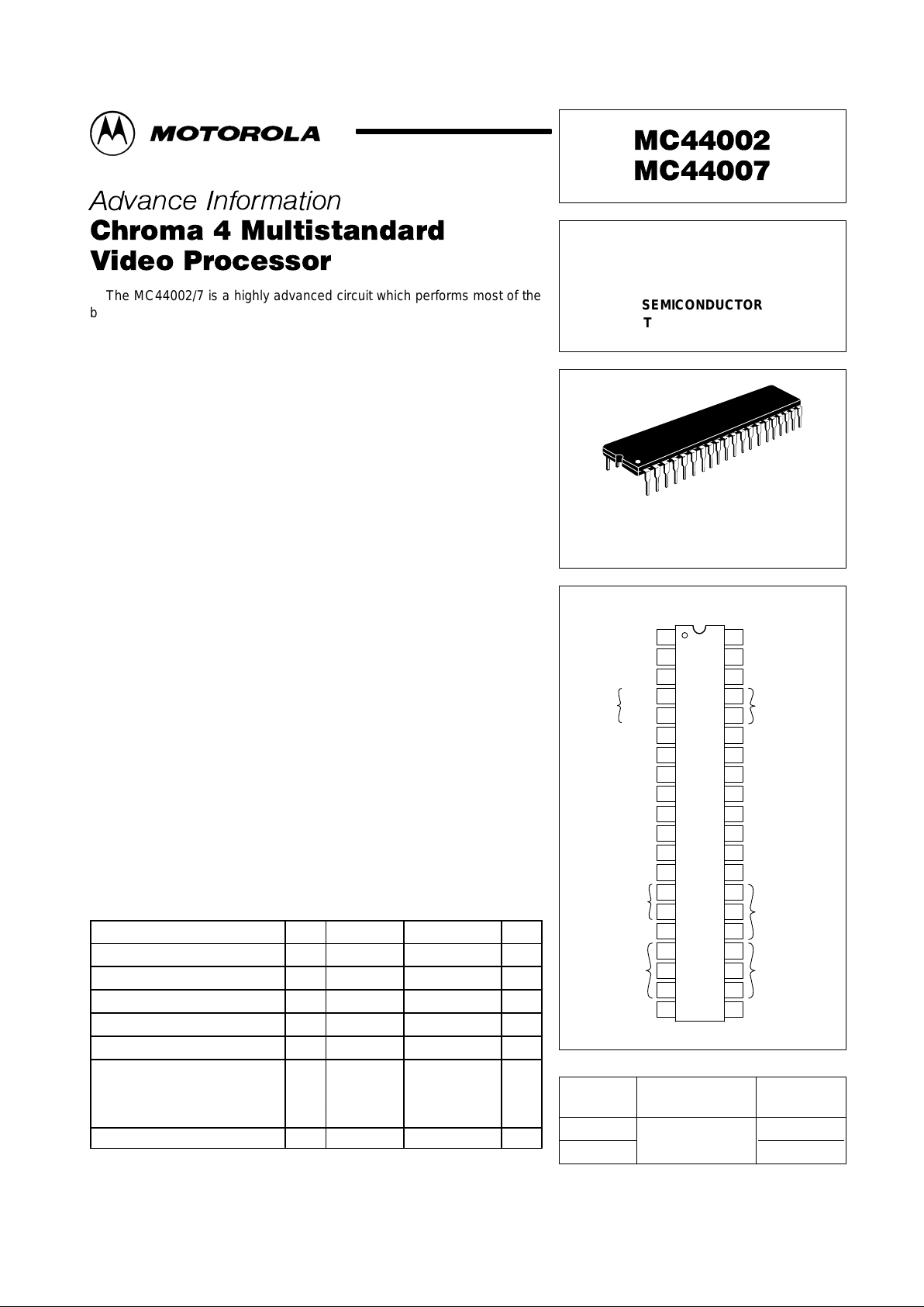
ORDERING INFORMATION
MC44002P
TA = 0° to +70°C
Plastic DIP
P SUFFIX
PLASTIC PACKAGE
CASE 711
40
1
PIN CONNECTIONS
Order this document by MC44002/D
38
40
39
37
36
35
34
33
32
31
30
29
28
27
26
25
24
23
22
21
9
10
11
12
13
14
15
16
17
18
19
20
1
2
3
4
5
6
7
8
(Top View)
ACC
Video 2
I
ref
Clock
Data
V-Ramp
V-Drive
E-W Drive
Osc Loop Filter
Ident
R-Y
B-Y
V
CC
Gnd
(17.7 MHz)
I
Anode
Analog Contrast
SECAM Cal Loop
H-Drive
H-Flyback Input
2
1
(14.3 MHz)
Sandcastle
System Select
Y1 Output
Y1 Clamp
R-Y
B-Y
Signal Gnd
R
G
B
Feedback
Y2
R
G
B
Fast Commutate
Outputs
H-Loop Filter
Inputs
Inputs
Crystals
Outputs
Video 1 In
I2C
MC44007P Plastic DIP
1
MOTOROLA ANALOG IC DEVICE DATA
The MC44002/7 is a highly advanced circuit which performs most of the
basic functions required for a color TV . All of its advanced features are under
processor control via an I2C bus, enabling potentiometer controls to be
removed completely. In this way the component count may be reduced
dramatically , allowing significant cost savings together with the possibility of
implementing sophisticated automatic test routines. Using the MC44002/7,
TV manufacturers will be able to build a standard chassis for anywhere in the
world. Additional features include 4 selectable matrix modes (primarily for
NTSC), fast beam current limiting and 16:9 display.
• Operation from a Single 5.0 V Supply; Typical Current Consumption
Only 120 mA
• Full P AL/SECAM/NTSC Capability (4 Matrix Modes)
• Dual Composite Video or S-VHS Inputs
• All Chroma/Luma Channel Filtering, and Luma Delay Line Are
Integrated Using Sampled Data Filters Requiring No External
Components
• Filters Automatically Commutate with Change of Standard
• Chroma Delay Line is Realized with a 16 Pin Companion Device, the
MC44140
• RGB Drives Incorporate Contrast and Brightness Controls and Auto
Gray Scale
• Switched RGB Inputs with Separate Saturation Control
• Auxiliary Y, R-Y, B-Y Inputs
• Line Timebase Featuring H-Phase Control, T ime Constant and
Switchable Phase Detector Gain
• Vertical Timebase Incorporating Vertical Geometry Corrections
• 16:9 Display Mode Capability
• E-W Parabola Drive Incorporating Horizontal Geometry Corrections
• Beam Current Monitor with Breathing Compensation
• Analog Contrast Control, Allowing Fast Beam Current Limitation
• MC44007 Decoders P AL/NTSC Only
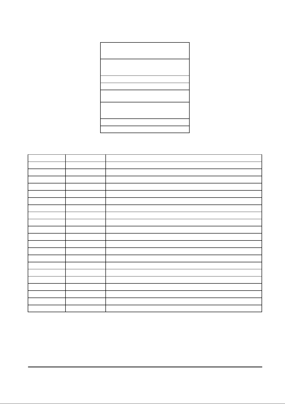
MAXIMUM RATINGS
(TA = 25°C, unless otherwise noted.)
Rating
Pin Symbol Value Unit
Supply Voltage 35 V
CC
6.0 Vdc
Operating Ambient Temperature – T
A
0 to + 70 °C
Storage Temperature – T
stg
– 65 to +150 °C
Junction Temperature – T
J
+150 °C
Drive Output Sink Current 12 I
12
2.0 mA
Applied Voltage Range: Vdc
Feedback 20 V
20
0 to +8.0
Anode Current 9 V
9
– 2.0 to V
CC
All Other Pins – V
i
0 to V
CC
ESD V
NOTE: ESD data available upon request.
This document contains information on a new product. Specifications and information herein
are subject to change without notice.
Motorola, Inc. 1996 Rev 1
Page 2
MC44002 MC44007
2
MOTOROLA ANALOG IC DEVICE DATA
MAXIMUM RATINGS
(TA = 25°C, unless otherwise noted.)
Rating UnitValueSymbolPin
Human Body Model – – ±2000
Machine Model – – ±200
NOTE: ESD data available upon request.
Chroma
T ake–Of f
Filter
Matrix
Switching
&
RGB Sat
Control
Luma
Select
17.7 MHz
Video 1
(S-VHS)
Video 2
Y2
R-Y
B-Y
Fast Comm.
Filter
Filter
System
Select
Sat &
Hue
System
R-Y B-Y Y1
Memory/Control Registers
Y1
Clamp
Parab
Gen
Beam
Current
Monitor
Control
Loops
Rx/Tx
Red
Green
Blue
Red
Green
Blue
RGB
Outputs
Analog
Contrast
FdbckDataClk
Anode
Current
E-W
Drive
Freq
Divider
Flyback
Sense
14.3 MHz
Loop
2
H Flyback
Pulse
H Drive
5.0 V
V Drive
5.0 V
I
ref
V
Sync
PAL/
NTSC/
SECAM
Decoder
Ident
Clk
Vert
Sync
Sep
Osc
PLL 1
Ramp
Gen
Luma Delay
Peaking & Trap
ACC
SandCastle
Sync
Sep
Input
Select
240
31
13038 37 36 29
14
15
39
32
33
25
27
26
28
21
24
22
17
18
19
16
10
205498637131235
34
23
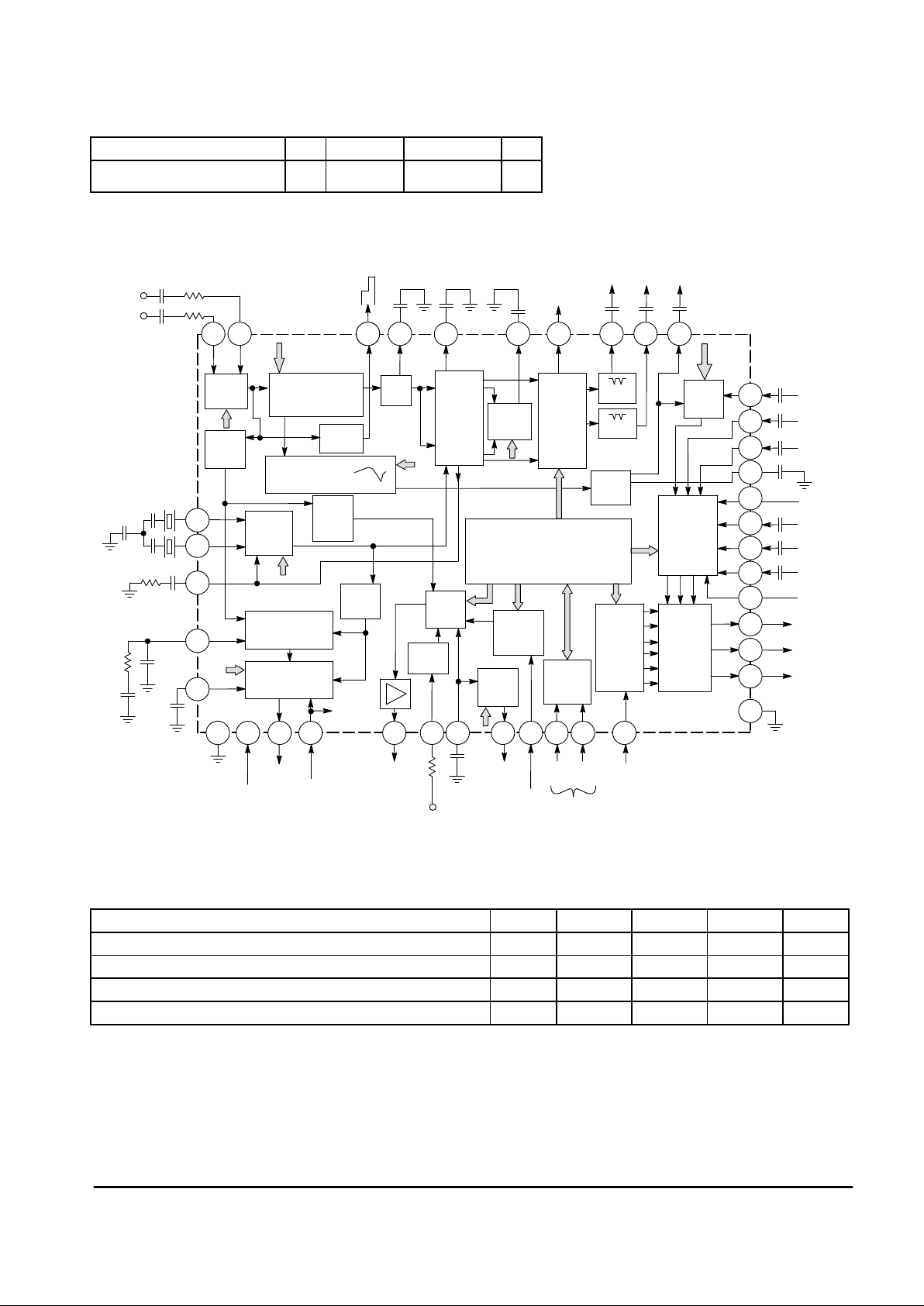
Simplified Block Diagram
11
I2C
Bus
This device contains 6,245 active transistors.
ELECTRICAL CHARACTERISTICS (V
CC
= 5.0 Vdc, I3 = 70 µA, TA = 25°C, unless otherwise noted.)
Characteristic
Pin Min Typ Max Unit
Supply Voltage 35 4.75 5.0 5.25 V
Operating Current 35 90 120 180 mA
Reference Current, Input Voltage 3 1.0 1.3 1.6 V
Thermal Resistance, Junction–to–Ambient – – 56 – °C/W
NOTES: Composite Video Input Signal Level = 1.0 Vpp Horizontal Timebase started (subaddress 00)
Black-to-White = 0.Vpp7 , Syn-to-Black = 0.3 Vpp Vertical Breathing control set to 00; V9 = 0 V
PAL/NTSC = 75% color bars; Burst = 300 mVpp All other analog controls set to midrange 32
SECAM = 75% color bars Video Peaking “P1, P2, P3” bits high
Page 3
MC44002 MC44007
3
MOTOROLA ANALOG IC DEVICE DATA
TEST CONDITIONS (unless otherwise noted.)
VCC = 5.0 V
I
ref
= 70 µA
TA = 25°C
Video Composite Input = 1.0 Vpp
– Black–to–White = 0.7 Vpp
– Black–to–Sync = 0.3 Vpp
Horizontal Timebase Started (Reg. 00)
Vertical Breathing Control Set to 00
Pin 9 = 0 V
Pin 10 = 5.0 V
PAL/NTSC = 75% Color Bars
–Burst = 300 mVpp
SECAM = 75% Color Bars (MC44002 only)
All Analog Controls Set to Midpoint (32)
Luma Peaking at Min. (P1 – P3 = 111)
Control Bits Setup
Name Value Function Status
V1/V2 1 Video Input 1 Selected
H EN 0 Horizontal Drive Enabled
BRI EN 1 “Bright” Sample “On”
HGAIN1 0 Horizontal Phase Detector Gain Reduced by 3 Enabled
YX EN 0 Luma Matrix Disabled
Y1 EN 1 Luma from Filters “On”
D EN 0 RGB Inputs Enabled
XS 0 Pin 33 Crystal Enabled
TEST 1 Outputs Sampled Once/Field
FSI 0 50 Hz Field Rate
T3 1 Low Pass Filter Enabled
VD1 1 4:3 Display Mode
2xFh 0 Horizontal Drive at 1xFh
NORM 0 Horizontal Reference Divider for 17.7 MHz
HGAIN2 1 Horizontal Phase Detector Gain Reduced by 2 Enabled
INTSEL 1 Long Vertical Time Constant
Y2 EN 0 External Luma Input “Off”
SSD 0 SECAM Mode Select Enabled
CALKIL 1 Horizontal Calibration Loop Enabled
BAI 1 Vertical Blanking for 625 Lines
S–VHS 1 Composite Video Input
Page 4
MC44002 MC44007
4
MOTOROLA ANALOG IC DEVICE DATA
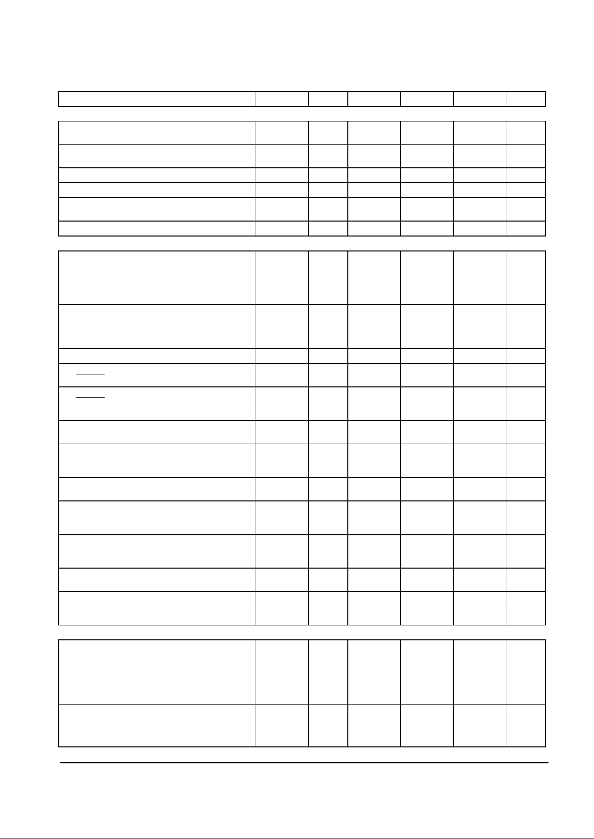
ELECTRICAL CHARACTERISTICS
Parameter Symbol Pin Min Typ Max Unit
BUS REQUIREMENTS
Maximum Output Low Voltage V
OL(max)
5 – 0.7 – V
I
sink
= 1.0 mA, Device in “Read” Mode
Maximum Sink Current I
sink(max)
5 – 1.0 – mA
VOL = 0.7 V , Device in “Read” Mode
Minimum Input High Voltage V
IH(min)
5 – 3.0 – V
Maximum Input Low Voltage V
IL(max)
5 – 1.5 – V
Maximum Rise Time t
r(max)
4, 5 – 1.0 – µs
Between VIH and VIL Levels
SCL Clock Frequency f
SCL
4 – – 100 kHz
HORIZONTAL TIMEBASE
Free–Running Frequency (Calibration Mode) – 31 kHz
17.734475 MHz Crystal. “NORM” Bit = 0;
“H EN” Bit = 1 (Horizontal Drive Disabled)
15.39 15.625 15.85
14.31818 MHz Crystal. “NORM” Bit = 1;
“H EN” Bit = 1 (Horizontal Drive Disabled)
15.42 15.75 15.98
H–Loop 1 (Pin 15 Current Forced to ± 20 µA) – 12 kHz
Minimum Frequency 13.85 14.25 14.65
Maximum Frequency 16.05 16.55 17.05
Frequency Range – 2.3 –
VCO Control Gain – 12, 15 1.9 2.4 2.9 kHz/V
Phase Detector Gain – 15 18 27 39 µA/µs
“HGAIN1” Bit = 1; “HGAIN2” Bit = 0
Phase Detector Gain Reduction Factor – 15 –
“HGAIN1“ Bit Switched from 1 to 0 2.5 3.0 3.5
“HGAIN2“ Bit Switched from 0 to 1 1.75 2.0 2.25
Line Drive Output Saturation Voltage – 12 – 0.25 0.5 V
I12 = 1.0 mA
Horizontal Drive Pulse Low – 12 – 27 – µs
Defined by Internal Counter, Deflection Transistor
“Off”, Period is 64 µs
Horizontal Flyback Input Resistance – 13 – 50 – kΩ
V13 = 2.0 V
Horizontal Flyback Clamping Voltages – 13 V
I13 = 500 µA – 5.7 –
I13 = –50 µA – –0.5 –
Horizontal Flyback Threshold Current – 13 30 – – µA
Should be Externally Limited to 500 µA Peak by an
External Resistor
Horizontal Phase Control Range – 12 8.0 – 12 µs
Flyback Duration: 12 µs
External Delay Compensation – 12, 13 6.0 – 18 µs
From Horizontal Drive to Center of Flyback Pulse.
Flyback Duration: 12 µs
VERTICAL TIMEBASE (All Values are Related to Pin 3 Reference Current)
Vertical Drive Amplitude (4:3 Display) – 7 V
(00) 1.15 1.33 1.5
(32) 1.55 1.75 1.95
(63) 1.95 2.18 2.4
C6 = 82 nF, Assuming Zero Tolerance
Capacitance, “VDI” Set to “1”
Vertical Drive Amplitude Control Range (4:3 Display) – 7 0.75 0.85 1.0 V
C6 = 82 nF, Assuming Zero Tolerance Capacitance,
“VDI” Set to “1”, Vertical Amplitude Varied from
(00) to (63)
Page 5
MC44002 MC44007
5
MOTOROLA ANALOG IC DEVICE DATA
ELECTRICAL CHARACTERISTICS (continued)
Parameter UnitMaxTypMinPinSymbol
VERTICAL TIMEBASE (All Values are Related to Pin 3 Reference Current)
Ramp Amplitude Ratio Between 4:3 and 16:9 Display
Modes
– 7 0.7 0.8 0.9 –
Vertical Amplitude = (32)
Maximum Ramp Amplitude Change With 525/625
Mode Change
– 7 – 2.0 – %
Vertical Ramp Low Voltage (4:3 Display) – 7 – 0.65 – V
Pin 6 Voltage Set to 0 V, “VDI” Set to “1”, Vertical
Position = (00)
Vertical Ramp Low Voltage (16:9 Display) – 7 – 0.85 – V
Pin 6 Voltage Set to 0 V, “VDI” Set to “0”, Vertical
Position = (00), Measured After 16:9 Holding
Period
Vertical Ramp High Voltage – 7 – 4.15 – V
Pin 6 Open, “VDI” Set to “0” or “1”, Vertical
Position = (63)
Vertical Ramp Position Control Range – 7 ±0.5 ±0.75 ±1.0 V
Versus Vertical Ramp Voltage at Vertical Position
(32), Measured at Vm, “VDI” Set to “0” or “1”,
Vertical Position Varied from (00) to (63)
Vertical Ramp Clamping Duration (tc) – 7 – 512 – µs
Defined by Internal Counter
Maximum Output Source Current – 7 1.0 – – mA
Maximum Output Sink Current – 7 200 – – µA
Vertical Linearity – 7 –
(00) – 0.8 –
(63) – 1.1 –
Change in Ramp current as Pin 9 Current Varied from
0 to 6.4 µA
– 6 µA
Vertical Breathing Correction = (63) 0.15 0.75 1.3
Vertical Breathing Correction = (00) – 0 –
Gain V7/V6 – 6, 7 0.9 0.95 1.0 V/V
E–W CORRECTION (V6(b) = 0.2 V , V6(m) = 1.1 V, V6(e) = 2.0 V)
Horizontal Amplitude – 8 µA
(00) 0 0.2 20
(63) 150 300 –
Corner Correction = (00), Tilt = (32), Parabola
Amplitude = (00), Measured at Tm.
Parabola Amplitude – 8 µA
(00) 0 0.2 10
(63) 100 250 –
Corner Correction = (00), Horizontal Amplitude =
(32), Tilt = (32), Measured at Tb, Tm and T
e.
Corner Correction – 8 µA
(00) 0 0.2 10
(63) – –150 –30
Horizontal Amplitude = (63), Parabola Amplitude =
(00), Tilt = (32), Measured at Tb, Tm and Te.
Parabola Tilt – 8 –
(00) – 1.9 –
(63) – –1.9 –
Corner Correction = (00), Horizontal Amplitude =
(32), Parabola Amplitude = (32), Measured at Tb,
Tm and Te.
E–W Drive Output Voltage – 8 1.0 – V
CC
V
Page 6
MC44002 MC44007
6
MOTOROLA ANALOG IC DEVICE DATA
ELECTRICAL CHARACTERISTICS (continued)
Parameter UnitMaxTypMinPinSymbol
E–W CORRECTION (V6(b) = 0.2 V, V6(m) = 1.1 V, V6(e) = 2.0 V)
E–W DACs Differential Non–Linearity Error – 8 LSB
At Minor Transitions: Steps 0–1: 1–2; 3–4; 7–8;
15–16.
–1.0 – 1.0
At Major Transition: Step 31–32 –2.0 – 1.0
SYNC SEPARATOR
Sync Amplitude to Operate the Device – 2, 40 100 – – mV
From Black to Sync, Black Picture, Standard Timing
Specifications on Sync Signal
22, 23,
24, 25
– 160 –
Vertical Sync Separator Delay T ime: t
d
– 2, 40 µs
“INTSEL” = 0 – 36 –
“INTSEL” = 1 – 68 –
From Vertical Sync Pulse to Vertical Ramp Reset
Vertical Sync Window – 2, 40,
22, 23,
24, 25
448 – 740 Half
Lines
COMPOSITE VIDEO PROCESSING (All measurements in NORMAL mode, unless otherwise noted.)
Composite Video Input Amplitude – 2, 40 0.7 1.0 1.4 Vpp
Load Impedance 75 Ω, Less than 5% Distortion
Video 1/Video 2 Input Crosstalk – 29 – – –40 dB
@ f = (2.0 MHz), Measured on Y1 Output
Variable Input LPF Cut–Of f Frequency – 29 MHz
17.7 MHz Crystal Selected – 6.0 –
14.3 MHz Crystal Selected – 4.85 –
Chroma Subcarrier Rejection – 29 dB
PAL 4.43 MHz (17.7 MHz Crystal Selected) 25 30 –
NTSC 3.58 MHz (14.3 MHz Crystal Selected) 25 30 –
SECAM (FoR and FoB) (17.7 MHz Crystal Selected) 18 20 –
Y1 Output Resistance – 29 – – 300 Ω
Y1 Bandwidth (–3.0 dB) – 29 MHz
PAL
Minimum Peaking, “T3” Set to 1 (Input LPF “On”)
2.5 3.0 –
SECAM
Minimum Peaking, “T3” Set to 0 (Input LPF “Off”)
2.5 3.0 –
Luma Peaking Range – 29 6.0 8.5 – dB
Measured at 3.0 MHz, 17.7 MHz Crystal Selected
Luma Gain (@ 100 kHz) – 2, 40, 29 0.9 1.1 1.3 V/V
Overshoot – 29 – 5.0 – %
Peaking at Step 3 (100)
Source Impedance – 2, 40 0 – 1.5 kΩ
Luma Delay Range – 29 ns
PAL/SECAM (17.7 MHz Crystal Selected) – 280 –
NTSC 3.58 (14.3 MHz Crystal Selected) – 350 –
Video In to Luma Out Delay Difference Between PAL
and SECAM (MC44002 only)
– 29, 40 – 260 – ns
Luma Delay Minimum: (D1 D2 D3) = (0 0 0), Green
to Magenta Transition, “T3” Set to 1 in PAL, to 0 in
SECAM
PAL/NTSC DECODER
Chroma Output Variation – 36, 37 – – 3.0 dB
For a Burst Input Varied from 60 mV to 600 mV
Color Kill Attenuation – 36, 37 40 – – dB
Referred to Standard Color Video Input,
Monochrome Mode Selected
Page 7
MC44002 MC44007
7
MOTOROLA ANALOG IC DEVICE DATA
ELECTRICAL CHARACTERISTICS (continued)
Parameter UnitMaxTypMinPinSymbol
PAL/NTSC DECODER
Color Difference Output Distortion – 36, 37 – – 5.0 %
@ 1.5 V Output Signal
Residual Chroma Subcarrier Rejection – 36, 37 dB
PAL 40 – –
NTSC 40 – –
Referred to Video Input
Oscillator Pull–In Range – 32, 33 Hz
PAL ±350 – –
NTSC ±400 – –
Referred to Nominal Subcarrier Frequency, with
Ideal Xtal
R–Y, B–Y Channel Separation – 36, 37 30 – – dB
B–Y/R–Y Amplitude Ratio – 36, 37 – 1.3 – V/V
At Standard Color Bars Signal
B–Y/R–Y Amplitude Ratio Spread – 36, 37 –2.0 – 2.0 dB
At Standard Color Bars Signal
Minimum Burst Level for “ACC Active” Flag “On” – 2, 40 – 10 20 mVpp
Standard Set to PAL or NTSC, Increasing Burst
Level Steps
Minimum Burst Level for “PAL Identified” Flag “On” – 2, 40 – 5.0 20 mVpp
Standard Set to PAL or NTSC, Increasing Burst
Level Steps
Maximum Burst Level for “ACC Active” Flag “Off” – 2, 40 – 5.0 – mVpp
Standard Set to PAL or NTSC, Decreasing Burst
Level Steps
Maximum Burst Level for “PAL Identified” Flag “Of f” – 2, 40 – 1.0 – mVpp
Standard Set to PAL or NTSC, Decreasing Burst
Level Steps
(B–Y) Color Difference Output Levels – 36 0.7 1.1 1.5 V
Relative to 75% Color Bars
Hue DAC Control Range – 36, 37 ±20 – – Deg
Hue Control Register Varying from (00) to (63)
Chroma to Luma Delay – 29, 36 ns
PAL – 80 –
NTSC – 100 –
Measured on (B–Y) Output, Luma Delay Set to
Minimum: (D1 D2 D3) = (0 0 0), Green to Magenta
Transition, “T3” Set to 1
DELAY LINE CONTROL SIGNALS
System Select – 30
PAL – 75 400 mV
NTSC 1.4 1.65 1.9 V
SECAM (MC44002 only) 2.75 3.0 3.25 V
EXTERNAL 3.7 4.0 4.3 V
Sandcastle – 31
Level 1 3.7 4.0 4.3 V
Level 2 2.75 2.95 3.15 V
Level 3 1..3 1.55 1.8 V
Level 4 – 75 – mV
See Figure 4
Sandcastle – 31 µs
t1 5.0 6.0 7.0
t2 4.0 5.0 6.0
See Figure 4, Values Defined by Internal Counter
Page 8
MC44002 MC44007
8
MOTOROLA ANALOG IC DEVICE DATA
ELECTRICAL CHARACTERISTICS (continued)
Parameter UnitMaxTypMinPinSymbol
S–VHS VIDEO PROCESSING (S–VHS Set to 0, “T3” Set to 0)
Y1 Bandwidth – 29 3.2 3.5 – MHz
Luma Peaking Set to Minimum
Minimum Burst Level for “ACC Active” Flag “On” – 2, 40 – 10 20 mVpp
Standard Set to PAL or NTSC, Increasing Burst
Level Steps
Minimum Burst Level for “PAL Identified” Flag “On” – 2, 40 – 5.0 20 mVpp
Standard Set to PAL or NTSC, Increasing Burst
Level Steps
Maximum Burst Level for “ACC Active” Flag “Off” – 2, 40 – 5.0 – mVpp
Standard Set to PAL or NTSC, Decreasing Burst
Level Steps
Maximum Burst Level for “PAL Identified” Flag “Of f” – 2, 40 – 1.0 – mVpp
Standard Set to PAL or NTSC, Decreasing Burst
Level Steps
Video In to Luma Out Delay Difference Between
S–VHS and Normal Mode
– 2, 40, 29 – 310 – ns
Luma Delay Minimum in Normal Mode, Set to Step
6 in S–VHS Mode, Green to Magenta Transition,
“T3” Set to 1 in Normal Mode, to 0 in S–VHS Mode
Chroma to Luma Delay Difference Between S–VHS
and Normal Mode
– 29, 36,
2, 40
– 60 – ns
Measured on (B–Y) Output, Luma Delay Minimum
in Normal Mode, Set to Step 6 in S–VHS Mode,
Green to Magenta Transition, “T3” Set to 1 in
Normal Mode, to 0 in S–VHS Mode
SECAM DECODER (MC44002 ONL Y)
Minimum Subcarrier Level for “SECAM Identified”
Flag
– 2, 40 – 10 20 mVpp
Measured at foR
Color Kill Attenuation – 36, 37 40 50 – dB
Monochrome Mode Selected Referred to Color
Difference Output Signal with SECAM Selected
and Identified
Color Difference Zero Level Error – 36, 37 – ±1.0 ±3.0 %
Relative to 75% Color Bars, Difference Between
Signal Measured at t1 and Active Black Level
(Black Bar)
Color Difference Output Distortion – 36, 37 – – 5.0 %
Subcarrier Level at foR = 20–400 mV @ 1.5 V
Output Signal
Transient Response – ns
(B–Y) 36 – 650 800
(R–Y) 37 – 750 900
Generator Rise Time – 600 ns (B–Y), Green to
Magenta Transition, Measured Between 10% and
90% Levels
B–Y/R–Y Amplitude – 36, 37
Ratio – 1.3 – V/V
Ratio Spread –2.0 – 2.0 dB
Relative to 75% Color Bars
Residual Carrier and Harmonics (4.0 to 13.5 MHz) – 36, 37 – – 1.0 %
At Standard Color Bars Signal
(B–Y) Color Difference Output Levels – 36 – 1.1 – V
Relative to 75% Color Bars
PAL/SECAM Color Dif ference Ratio – 36 0.8 1.0 1.2 –
Nominal Input Signals
Page 9
MC44002 MC44007
9
MOTOROLA ANALOG IC DEVICE DATA
ELECTRICAL CHARACTERISTICS (continued)
Parameter UnitMaxTypMinPinSymbol
SECAM DECODER (MC44002 ONL Y)
Chroma to Luma Delay – 29, 36 – 420 – ns
Luma Delay Set to Minimum: (D1 D2 D3) = (0 0 0),
Green to Magenta Transition, “T3” Set to 0
Patterning – 36 – – 5.0 %
Full Screen 75% Color Frequency, 500 kHz Low
Pass Filter, Relative to Black to Color Output Signal
Line to Line Luma Levels Difference – 29 – – 1.5 %
Full Screen 75% Y ellow Color Frequency, Relative
to Black to Yellow Output Signal
Chroma to Luma Delay Difference Between P AL and
SECAM
– 29, 36 – 340 – ns
Measured on (B–Y) Output, Luma Delay Set to
Minimum: (D1 D2 D3) = (0 0 0), Green to Magenta
Transition, “T3” Set to 0 in SECAM, to 1 in PAL
COLOR DIFFERENCE STAGES
RGB Input Amplitude – 22, 23, 500 700 1000 mVpp
Black to Peak (Less than 5% Distortion at RGB
Outputs)
24
Fast Commutate – 21 V
Low Level – – 0.5
High Level 1.0 – –
Y2 Input Amplitude – 25 0.7 1.0 1.4 Vpp
(Less than 5% Distortion at RGB Outputs)
Color Difference Input Amplitude – 26, 27 – – 1.8 Vpp
(Less than 5% Distortion at RGB Outputs)
Y2/Y1 Crosstalk – 25, 29 – –40 –30 dB
Measured at RGB Outputs, Measured at f = (2.0 MHz)
RGB to Y Crosstalk – 22, 23, – –40 –30 dB
Measured at RGB Outputs, Measured at f = (2.0 MHz) 24, 25,
29
RGB Transconductance Bandwidth (@ –1.0 dB) – 24, 17,
23, 18,
22, 19
6.5 – – MHz
Gain Reduction in ACL Mode – 10, 17, – 12.5 – dB
Pin 10 Voltage Varying from 0 to 5.0 v 18, 19
Gain Reduction Sensitivity in ACL Mode – 10, 17, – 20 – dB/V
Pin 10 Voltage Varying from 2.0 to 2.5 V 18, 19
Demodulation Angles and Amplitudes – – Deg
Mode A Rm – 0.562 –
Ra – 90 –
Gm – 0.344 –
Ga – 237 –
Mode B Rm – 0.9 –
Ra – 100 –
Gm – 0.3 –
Ga – 236 –
Mode C Rm – 0.9 –
Ra – 106 –
Gm – 0.3 –
Ga – 240 –
Mode D Rm – 0.91 –
Ra – 106 –
Gm – 0.31 –
Ga – 246 –
Definitions: Rm/Gm = Module, Ra/Ga = Argument
Page 10
MC44002 MC44007
10
MOTOROLA ANALOG IC DEVICE DATA
ELECTRICAL CHARACTERISTICS (continued)
Parameter UnitMaxTypMinPinSymbol
RGB OUTPUT STAGES
Low Dark Sample Output Current – 17, 18, mA
Red 19 – – 3.15
Green – – 3.15
Blue – – 3.15
Dark Sample Cathode Current 5.0 to 15 µA, DC
DAC Set to Full Scale, See Figure 1
High Dark Sample Output Current – 17, 18, mA
Red 19 3.95 – –
Green 3.95 – –
Blue 3.95 – –
Dark Sample Cathode Current 5.0 to 15 µA, DC
DAC Set to Zero, See Figure 1
Blanking Output Current – 17, 18,
19
6.0 – – mA
Maximum Y to RGB Output Transconductance – 17, 18, 6.0 7.0 8.0 mA/V
Gain DAC Set to Full Scale 19
Brightness – – V
(00) – 30 –
(63) – –20 –
Wrt Dark Sample Cathode Voltage,
High Voltage Output Stage T ransimpedance
39 kΩ, Dark Sample Cathode Current 15 µA, Dark
Sample Cathode Voltage 140 V
RGB Dark Sample Current Intensity Range – 20 15 20 – dB
RGB Intensity DACs Varying from (00) to (63)
Bright to Dark Sample Current Ratio – 20 8.0 9.5 11 µA/µA
Leakage Loop – 20 µA
Sink Current 20 – –
Source Current 5.0 – –
Average Beam Current Detection Level – 9 V
Excess Flag 0.9 1.0 1.1
Overload Flag –1.3 –1.2 –1.1
Peak Beam Current Detection Level – 20 6.5 6.8 7.1 V
Figure 1. Example of Output Circuitry
Vp, V
ref
, R
FDBK
and Rp values will determine the exact operating point.
For example, let us take:
Vp = 5.0 V R
FDBK
= 39 kΩ
V
ref
= 3.6 V
Rp = 6.8 kΩ
The formula giving the Dark Cathode Voltage with above circuit is: Vdk = V
ref
+ R
FDBK
*(V
ref
– Vp + lodk*Rp) / R
p
With above application, component values and lodk specifications, all 3 cathodes on all devices will always have a range of at least 120 V to 150 V.
By changing the values of Vp, V
ref
and Rp, the cathode voltage range may be shifted up or down as required.
lodk
V
ref
V
dk
Picture Tube
Cathode
R
FDBK
R
P
V
P
Pins 17, 18, 19
MC44002/7P
Page 11
MC44002 MC44007
11
MOTOROLA ANALOG IC DEVICE DATA
Figure 2. Vertical Waveforms
Figure 3. Vertical Ramp Positions (V7 versus V6)
1.6 ms 18.4 ms
T
b
T
m
T
e
V
b
V
m
V
e
I
b
I
m
I
e
t
d
t
c
Video Signal
Vertical Ramp W aveform
Parabola Waveform
V Ramp High Voltage
V Ramp Low Voltage
(XX) = Values of (80) Register
(63)
Pin 6 Voltage (V)
Pin 7 Voltage (V)
4
1
(32) (00)
3
2
1
234
Page 12
MC44002 MC44007
12
MOTOROLA ANALOG IC DEVICE DATA
Definitions
Parabola Amplitude
+
(ib)
ie)
2
–i
m
Parabola Tilt
+
(ie–ib)
Parabola Amplitude
Horizontal Amplitude+i
m
Vertical Amplitude+Ve–V
b
Vertical Linearity
+
(Ve–Vm)
Vm–V
b
Corner correction is calculated in the same way as Parabola Amplitude.
Figure 4. Sandcastle Output (Pin 31)
64 µs
1
2
4
3
t1
t2
GENERAL DESCRIPTION OF THE CHROMA 4 SYSTEM
Figure 5 shows a simplified block diagram representation
of the basic system using the MC44002/7 and its companion
device the MC44140 chroma delay line. The MC44002/7 has
been designed to carry out all the processing of video
signals, display controls and timebase functions. There are
two video inputs which can be used for normal composite
video or separate Y and C inputs. In either case, the inputs
are interchangeable and selection is made via the I2C bus.
The video is decoded within the MC44002/7 and involves
separation, filtering, delay of the luminance part of the signal
and demodulation of the chroma into color difference signals.
The luminance (called Y1) together with the demodulated
R-Y and B-Y are all then brought out from the IC. The color
difference signals then enter the MC44140 which performs
color correction in PAL and the delay line function in SECAM.
Corrected color difference signals then re-enter the
MC44002/7.
Page 13

MC44002 MC44007
13
MOTOROLA ANALOG IC DEVICE DATA
Figure 5. Connection to TV Chassis
B
B
G
G
R
R
G2
G1
EHT
V O/P
Stage
V-Scan
Coils
26 V
Line O/P
Stage
E-W
Amplifier
Diode Modulator
Linearity
H-Scan
Coils
Focus
EHT
Tripler
5.0 V
Line Output
Transformer
H-Flyback
H-Drive
Anode Current
E-W Drive
V-Drive
Analog
Contrast
R-O/P
G-O/P
B-O/P
Feedback
0 V
Data
Clock
14.3 MHz
17.7 MHz
Fast Commutate
B In
G In
R In
Y2 In
Ext B-Y
Ext R-Y
B-Y In
R-Y In
B-Y Out
R-Y Out
Y1 Out
Video 2
Video 1
G3
I2C Bus
MC44002/7
MC44140
H.T.
Comp Video
or
S-VHS
Beam Current
Limitation
12 V
The next stage is called the color difference stage where a
number of control functions are carried out together with
matrixing of the components to derive RGB signals. At this
point a number of auxiliary signals may also be switched in,
again all under MCU control. External RGB (text) and Fast
Commutate enter here; also an external luminance (Y2) may
be used instead of Y1. External R-Y and B-Y are switched in
via the delay line circuit to save pins on the main device. The
Y2 and External R-Y, B-Y will obviously be of considerable
benefit from the system point of view for use with external
decoders.
The final stage of video processing is the RGB outputs which
drive the high voltage amplifiers connected to the tube
cathodes. These outputs are controlled by a sophisticated
digital servo-loop which is maintained and stabilized by a
sequentially sampled beam current feedback system.
Automatic gray scale control is featured as a part of this system.
Both horizontal and vertical timebases are incorporated
into the MC44002/7 and control is via the I2C bus. The
horizontal timebase employs a dual loop system of a PLL and
variable phase shifter, and the vertical uses a countdown
system. For the vertical, a field rate sawtooth is available
which is used to drive an external power amplifier with
flyback generator (usually a single IC). The line output
consists of a pulse which drives a conventional line output
stage in the normal way. The line flyback pulse is sensed and
used by the second loop for horizontal phase shift.
Where E-W correction is required, a parabola waveform is
available for this which, with the addition of a power amplifier,
can be used with a diode modulator type line output stage for
dynamic width and E-W control. The bottom of the EHT
overwinding is returned to the MC44002/7 and is used for
anode current monitoring.
Fast beam current limitation is also made possible by the
use of an analog contrast control.
A much more detailed description of each stage of the
MC44002/7 will be found in the next section. Information on
the delay line is to be found in its own data sheet.
Page 14

MC44002 MC44007
14
MOTOROLA ANALOG IC DEVICE DATA
Introduction
The following information describes the basic operation of
the MC44002/7 IC together with the MC44140 chroma delay
line. The MC44002/7 is a highly advanced circuit which
performs all the video processing, timebase and display
functions needed for a modern color TV . The device employs
analog circuitry but with the difference that all its advanced
features are under processor control, enabling external
filtering and potentiometer adjustments to be removed
completely. Sophisticated feedback control techniques have
been used throughout the design to ensure stable operating
conditions and the absence of drift with age.
The IC described herein is one of a new generation of TV
circuits, which make use of a serial data bus to carry out
control functions. Its revolutionary design concept permits a
level of integration and degree of flexibility never achieved
before. The MC44002/7 consists of a single bipolar VLSI chip
which uses a high density, high frequency, low voltage
process called MOSAIC 1.5. Contained within this single 40
pin package is all the circuitry needed for the video signal
processing, horizontal and vertical timebases and CRT
display control for today’s color TV. Furthermore, all the user
controls and manufacturer’s set-up adjustments are under
the control of the processor I2C bus, eliminating the need for
potentiometer controls. The MC44002/7 offers an enormous
variety of different options configurable in software, to cater
to virtually any video standard or circumstance commonly
met. The decoder section offers full multistandard capability,
able to handle PAL, SECAM (MC44002 only) and NTSC
standards with 4 matrix modes available. Practically all the
filtering is carried out onboard the IC by means of sampled
data filters, and requires no external components or
adjustment.
Digital Interface
One of the most important features of MC44002/7 is the
use of processor control to replace external potentiometer
and filter adjustments. Great flexibility is possible using
processor control, as each user can configure the software to
suit their individual application. The circuit operates on a
bidirectional serial data bus, based on the well known I2C
bus. This system is rapidly becoming a world standard for the
control of consumer equipment.
I2C Bus
It is not within the scope of this data sheet to describe in
detail the functioning of the I2C bus. Basically, the I2C bus is
a two-wire bidirectional system consisting of a clock and a
serial data stream. The write cycle consists of 3 bytes of data
and 3 acknowledge bits. The first byte is the Chip Address,
the second the Sub-address to identify the location in the
memory, and the third byte is the data. When the address’
Read/Write bit is high, the second and third bytes are used to
transmit status flags back to the MCU.
Figure 6 shows a block diagram of the MC44002/7 Bus
Interface/Decoder. To begin with, the start bit is recognized
by means of the data going low during CLK high. This causes
the Counter and all the latches to be reset. For a write
operation, the Write address ($88) is read into the Shift
Register. If the correct address is identified, the Chip Address
Latch is set and at CLK 9 an acknowledge is sent.
The second byte is now read into the Shift Register and is
used to select the Sub-address. At CLK 18 a Sub-address
Enable is sent to the memory to allow the Data in the register
to be changed. Also, at CLK 18 another acknowledge is sent.
The third byte is now read into the Shift Register and the
Data bussed into the memory. The Data in the Sub-address
location already selected is then altered. A third acknowledge
is sent at CLK 27 to complete the cycle.
A Read address ($89) indicates that the MCU wants to
read the MC44002/7 status flags. In this instance, the
Read/Write Latch is set, causing the Memory Enable and
Subaddress Enable to be inhibited, and the flags to be written
onto the data line. Two of the status flags are permanently
wired one-high and one-low (O.K. and Fault), to provide a
check on the communication medium between the
MC44002/7 and the MCU.
At start-up the Counter is automatically reset and the Data
for each Sub-address is read in from the MCU. Only after the
entire memory contents have been transmitted, is Data 00
sent to register 00 to start the Horizontal Drive.
The MC44002/7 needs the full 27 clock cycles, or a stop
condition, to properly release the I2C bus.
4
Figure 6. I2C Bus Interface and Decoder
8-Bit Shift Register
Read/Write
Latch
Chip-Address
Latch
Sub-Address
Latches
Memory &
Sub-Address
Decoding
Acknowledge
Data
Clock
Clock Counter
Reset
Start-Bit
Recognition
5
8-Bit
8-Bit
8-Bit
Page 15

MC44002 MC44007
15
MOTOROLA ANALOG IC DEVICE DATA
A
D
Bits 6,7Bits 6,7Bits 6,7Bits 6,7Bits 6,7
I-88I-87I-7AI-79I-78
Figure 7. MC44002/7 Memory Map
Data 0
Data 1
Data 2
Data 3
Data 4
Data 5
Data 6
Data 7
MSB
LSB
A
D
A
D
A
D
A
D
Memory Sub-Address 77
Digital Register, Bits 0-7
Memory Sub-Address 78
Analog Register, Bits 0-5
Memory Sub-Address 79
Analog Register, Bits 0-5
Memory Sub-Address 7A
Analog Register, Bits 0-5
Memory Sub-Address 87
Analog Register, Bits 0-5
Memory Sub-Address 88
Analog Register, Bits 0-5
Memory
Figure 7 shows a diagram of the MC44002/7 Memory
Map. It has 18 bytes of memory which are located at hex
sub-addresses 77 to 88. Sub-address 77 is used to set up the
vertical timebase mode of the IC and for S-VHS switching,
and consists of 8 separate data bits. The remaining 17 bytes
use the least significant 6-bits as an analog control register.
The contents of each are D/A converted, providing an analog
control current which is distributed to the appropriate part of
the circuit. Bits 6 and 7 are used singularly for switching
control functions.
Chroma Decoder
The main function of this section is to decode the incoming
composite video, which may be in any of the PAL, NTSC or
SECAM (MC44002 only) Standards, and to retrieve the
luminance and color difference signals. In addition, the signal
filtering and luma delay line functions are carried out in this
section by means of sampled data filters.
The entire decoder section operates in sampled data
mode using clocks generated by external crystals. The
oscillator, which is phase-locked in the usual way for
PAL/NTSC modes, provides the clock function for the whole
circuit. The crystals are selected by the MCU by means of a
control bit (XS). Only crystals appropriate to the standards
which are going to be received need to be fitted. A 17.7 MHz
crystal (4x PAL subcarrier) is used for PAL and SECAM
systems (50 Hz, 625 lines); and 14.3 MHz (4x NTSC
subcarrier) for the NTSC system (60 Hz, 525 lines). Nearly all
the filters, together with the luma delay line and peaking,
have been integrated, requiring no external components or
any adjustment. The filter characteristics are entirely
determined by the clocks and by capacitor ratios, and are
thus completely independent of variations in the
manufacturing process. The PAL/NTSC subcarrier PLL and
ACC loop filters have not been integrated in order to facilitate
testing. These filters consist of fixed external components.
Figure 8 is a block diagram of the main features of the
chroma decoder. Selection is first made between the Video 1
and Video 2 inputs. These may be either normal composite
video or separate luma and chroma which may enter the IC at
either pin. Commands from the MCU are used to route the
signals through the appropriate delay and filter sections.
In PAL/NTSC, a variable low pass filter, which can be
software bypassed (control bit T3), is then used to
compensate for IF filtering and the Q of the external sound
traps. Filter response is controlled by means of control bits
T1 and T2. It is not recommended to use this filter in SECAM
or in S–VHS, as luma–chroma delays will not be optimized.
Next, the video enters the luma path. The PAL/NTSC or
SECAM chroma signals are separated out by transversal
high pass filters. In SECAM mode, the chroma trap frequency
is dynamically steered to follow the instantaneous frequency
of the chroma.
Then, another transversal filter provides luma peaking,
which is also active in S–VHS mode. The high frequency
luma may be peaked (at about 3.0 MHz with the 17.7 MHz
crystal, and 2.4 MHz with the 14.3 MHz crystal) in 7 steps up
to a maximum of 8.5 dB, by a control word from the MCU.
Another control word is used to trim the delay in the luma
channel. Five steps of 56 ns (70 ns with the 14.3 MHz crystal)
are possible, giving a total programmable delay of 280 ns.
Steps 6 and 7 are used in S–VHS mode. The resulting
processed luma signal then proceeds to the color difference
section after being low–pass filtered by an active filter to
remove components of the crystal frequency, and twice that
frequency. The luma component (Y1) is made available at
Pin 29 for use with auxiliary external functions, as well as
testing.
When in the S–VHS mode, the S–VHS control bit controls
the signal paths. The luma signal bypasses the first section of
the luma channel, which contains the chroma trap. The
S–VHS chroma is passed directly to the PAL/NTSC decoder
without further filtering.
As all the delay and filter responses are determined by the
crystal, they automatically commute to the new standard
when the crystal is changed over. Thus, when the 14.3 MHz
clock is being used, the chroma trap moves to 3.58 MHz.
The filtered PAL/NTSC and SECAM chroma signals are
decoded by their respective circuits. The P AL/NTSC decoder
employs a conventional design, using ACC action for gain
control and the common double balanced multipliers to
retrieve the color difference signals. The SECAM decoder is
discussed in a separate subsection.
Page 16

MC44002 MC44007
16
MOTOROLA ANALOG IC DEVICE DATA
PAL/NTSC
(MCU)
29
36
37
391
B-Y
R-Y
SECAM
Decoder
32
33
Oscillator
14.3MHz
17.7MHz
C
C
PLL
ACC
PAL/NTSC Decoder
4.4/8.8MHz
R-Y
System Select
Hue Controls
V
U
Ident
(MCU)
B-Y
4.4/8.8MHz
Luma
Luma
Delay
Line
Ident Data
(MCU)
Luma–Chroma Filters
t1, t2
Video 2
Video 1
38
Figure 8. Chroma Decoder
AGC Q
S-VHS
Crystal
Select
S-VHS
Delay ADJ
To Color
Difference
Stage
11
SECAM
Cal
Loop
2
40
Peaking
Syn
Sep
t3
Input
Select
Y1
NOTES: SECAM decoding
available in the MC44002 only.
The actual decision as to a signal’s identity is made by the
MCU based on data provided by 3 flags returned to it,
namely: ACC Active, PAL Identified, and SECAM Identified.
Control bits SSA–SSD must be sent to set the decoder to
the correct standard.
This allows a maximum of flexibility, since the software
may be written to accommodate many different sets of
circumstances. For example, channel information could be
taken into account if certain channels always carry signals in
the same standard. Alternatively, if one standard is never
going to be received, the software can be adapted to this
circumstance. If none of the flags are on, color killing can be
implemented by the MCU. This occurs if the net Ident Signal
is too low, or if the ACC circuit is inactive due to too low a
signal level.
The demodulated color difference signals now enter the
Hue control section, where selection is made between
PAL/NTSC and SECAM outputs. The Hue control is simply
realized by altering the amplitudes of both color difference
signals together. Hue control is only a requirement in NTSC
mode and would not normally be used for other standards.
The function is usually carried out prior to demodulation of
the chroma by shifting the phase of the subcarrier reference,
causing decoding to take place along different axes. In the
MC44002/7, Hue control is performed on the already
demodulated color difference signals. A proportion of the R-Y
signal is added or subtracted to the B-Y signal and
vice-versa. This has the same effect as altering the reference
phase. If desired, the MC44002/7 can apply the Hue control
to simple PAL signals.
After manipulation by the Saturation and Hue controls, the
color difference signals are finally filtered to reduce any
remaining subcarrier and multiplier products. Before leaving
the chip at Pins 36 and 37, the signals are blanked during line
and frame intervals. The 64 µs chroma delay line is carried
out by a companion device, the MC44140.
SECAM Decoder (MC44002 only)
The SECAM signal from the high-pass filter enters tightly
controlled AGC amplifiers wrapped around a cloche filter
which is a sampled recursive type, with the AGC derived from
a signal squarer. Next, the signal is blanked during the
calibration gate period and a reference 4.43 MHz is inserted
during this time. The SECAM signal is then passed through a
limiter.
The frequency demodulator function is carried out by a
frequency-locked-loop (F.L.L.). This consists of three
components: a tracking filter, a phase detector and a loop
filter. The center frequency of the tracking filter depends on
three factors: internal R-C product, ADJUST voltage, and
TUNING voltage. The tracking filter is dynamically tuned by
the TUNING feedback from the loop-filter forming the F.L.L.
The ADJUST control calibrates the F.L.L. and compensates
for variations in the R-C product. After the F.L.L., the color
difference signals are passed to another block where several
functions are carried out. The signals are de-emphasized
and outputs are provided to the Ident section. Another
function of this section is to generate the I
COMP
signal used
for calibrating the F.L.L. This signal is blanked during the
H-IG period to ensure that (R-Y) and (B-Y) output signals
have a clean dc level for clamping purposes.
In addition, components are added to compensate for the
R-C product, and tuning offsets are introduced during the
active lines for F0R/F0B.
Calibration of the F.L.L. takes place during every field
blanking interval, starting from field retrace and ending just
before the SECAM vertical Ident sequence (bottles). The
calibration current I
CAL
is derived from I
COMP
during the
Page 17

MC44002 MC44007
17
MOTOROLA ANALOG IC DEVICE DATA
calibration gate (CAL) and integrated by an external
capacitor on Pin 11. The resulting voltage V
EXT
is then
transformed to generate the ADJUST control voltage
removing from the loop range most of the variations due to
internal RC products and temperature.
Color Difference Stages
This stage accepts luminance and color difference
signals, together with external R,G,B and Fast Commutation
inputs and carries out various functions on them, including
clamping, blanking, switching and matrixing. The outputs,
consisting of processed R,G,B signals, are then passed to
the Auto Gray Scale section.
A block diagram of this stage is shown in Figure 10. The
Y2, R-Y, B-Y together with R, G and B are all external inputs
to the chip. The Y1 signal comes from the decoder section.
Each of the signals is back-porch clamped and then blanked.
The Y2 and R,G,B inputs have their own simple sync
separators, the output from which may be used as the
primary synchronization for the chip by means of commands
from the MCU.
The Fast Commutation is an active high input used to drive
a high speed switch; for switching between the Y and color
difference inputs and the R,G,B (text) inputs.
After blanking, the Y1 and Y2 channels go to the Luma
Selector which is controlled by means of 2 bits from the MCU.
From here the selected luma signal goes to the RGB matrix.
The two color difference signals pass through the saturation
control. From here they go to a matrix in which G-Y is
generated from the R-Y and B-Y, and lastly , to another matrix
where Y is added to the three color difference signals to
derive R,G,B.
Control bits (via the I2C bus) allow the matrix coefficients
to be adjusted in order to suit different requirements,
particularly in NTSC. Table 1 shows the theoretical
demodulation angles and amplitudes and the corresponding
matrix coefficient values for each of the 4 selectable modes.
(The A mode corresponds to the standard PAL/SECAM/NTSC
mode). Although primarily intended for NTSC, this feature can
also act on PAL/SECAM or external RGB signals.
The R,G,B inputs may take one of two different paths.
They may either go straight to the output without further
processing, or via a separate matrix and the saturation
control. The path taken is controlled in software. When the
latter route is selected, the R,G,B signals undergo a matrix
operation to derive Y. From this, R-Y and B-Y are easily
derived by subtraction from R and B; the derived color
difference signals are then subjected to saturation control.
This extra circuitry allows another feature to be added to the
TV set, namely the ability to adjust the color saturation of the
RGB inputs. After the saturation control the derived signals
are processed as before.
Table 1. Matrix Modes Coefficients
A B C C
RR 1.0 1.577 1.539 1.556
RB 0 –0.156 –0.248 –0.251
GR –0.513 –0.443 –0.462 –0.504
GB –0.187 –0.168 –0.150 –0.125
BB 1.0 1.0 1.0 1.0
BR 0 0 0 0
Rm 0.562 0.9 0.9 0.91
Gm 0.344 0.3 0.3 0.31
Ra 90 100 106 106
Ga 237 236 240 246
NOTE: BB = Gain of (B
out
/(B–Y)in) = 1 (reference). BR = Gain of (B
out
/(R–Y)in) = 0 (theoretically).
Figure 9. SECAM Decoder (MC44002 only)
SECAM
I/P
VA1 Adjust
RC-T
Compensation
Ident
Out
De-emphasis
Tuning Offsets
Output Interface
PHIG
I
RC
Fbk
I
COMP
CAL
11
SECAM
Cal
Loop
I
CAL
AGC
A1 A2
CAL
X
2
Squarer
Timing SignalsSECAM Out
(R-Y/B-Y Sequen.)
FLL Demodulator
Phase
Detector
FLL Tracking
Filter
Loop
Filter
Cloche Filter
H
H Clamp
Calibration
Switch
Adjust
4.43MHz
Limiter
V
Tun
Page 18

MC44002 MC44007
18
MOTOROLA ANALOG IC DEVICE DATA
Clamp
Clamp
Clamp
Blanking
26
25
Y1
Sync
Separator
Clamp
Y1, Y2 Select
Luma
Selector
Gate
Outputs
19
18
17
Gate
Gate
R-Y
Gen
B-Y
Gen
R
G
B
Y Matrix
Blanking/Fast
Commutation
Logic
Blanking
Burst Gate
Bypass
YX EN
Blanking
Sync
Separator
ClampClampClamp
22232421
Fast
Commutation
Y2
Y1
Saturation
Control
Figure 10. Color Difference Stages
Matrix
28
Inputs
27
BGRF/C
B
G
R
B-Y
Y2
R-Y
Y1 Clamp
Analog
Contrast
10
BCL
Inputs
Page 19

MC44002 MC44007
19
MOTOROLA ANALOG IC DEVICE DATA
In order to implement automatic beam current limiting
(BCL), the possibility of fast contrast reduction has been
added. For normal operation, the Contrast control is
achieved by auto grey scale output loops and is I2C bus
controlled (see Section 4). In the case of excess beam
current, this control is not fast enough to protect the tube and
power supply stages. It is now possible, by acting on the
Pin 10 voltage, to reduce the contrast about 12 dB by
reducing the luma gain and saturation. In the case of direct
RGB mode, the RGB gains are also reduced.
Figure 11. Typical Contrast Reduction
PIN 10 VOLTAGE (V)
0 1.0 2.0 3.0 4.0 5.0
1.0
–1.0
–3.0
–5.0
–7.0
–9.0
–11
–13
RELATIVE CONTRAST LEVEL (dB)
Figure 11 is showing the typical analog CONTRAST
reduction possible as a function of the voltage on Pin 10. Two
solutions are possible for obtaining the BCL function:
1st solution:
A measure of the average and/or peak beam
current is applied to Pin 10, which causes a reduction of the
RGB drive levels to the high voltage video amplifiers. In this
case, no software control is required, but variations in color
balance and saturation may be observed. A typical
application is shown in Figure 12.
2nd solution:
The beam current flags are read and acted
on by the MCU, which reduces the I2C bus CONTRAST
control to maintain the average beam current below the
desired level. In the case of rapid and extreme beam current
changes (black to white picture at high contrast level), the
circuit of Figure 12 may be used as a fast aging protection
while the MCU is reducing the CONTRAST through I2C bus.
The average of this method is to make any color
balance/saturation variation only transient.
Figure 12. Automatic Beam
Current Limiter Application
470 n
270 k
R8 R9
1.0 M
R4
10 k
R1
C2 C3
12 V
2.2 M
C5C1 10 n
EHT
R3
33 k
10 n 4.7
µ
D1
1N4148
910
Auto Gray Scale Control Loops
This section supplies current drives to the RGB cathode
amplifiers and receives a signal feedback from them,
proportional to the combined cathode currents. The current
feedback is used to establish a set of feedback loops to
control the dc level of the cathode voltage (cut–off), and gain
of the signal at the cathode (white balance). There are three
loops to control the dark currents dark loops and another
three to control the gains bright loops. The system uses 3
lines at the end of the vertical suppression period and just
before the beginning of the picture for sampling the cathode
current (i.e., one line for red, one for green and one for blue).
The first half of reach line is used for adjusting the gain of the
channel and is usually called the “bright” adjustment period.
The second half of the line is used for adjusting the dc level of
the channel and is called the “dark” adjustment.
The theoretical circuit diagram for one channel is shown in
Figure 13 along with the basic equations. The dc level (ldc)
and gain (G) are both controlled by 7 bit DACs which receive
data directly from latches in which the required values are
stored between sampling periods.
Figure 13. Bright/Dark Current Control
Brightness (B)
I
Cont
Pins 17,
18 or 19
Bright
Dark
Bright Dark
I
Pict
Gain (G) Output Buffer (A)
I
O
I
DC
Picture Output Current: I
O(Pict)
= A x [ IDC = G x ((B x I
Cont
) + I
Pict
)]
Dark Sample Output Current: I
O(dk)
= A x I
DC
Bright Sample Output Current: I
O(br)
= I
O(dk)
– A x G X I
Cont
Black Level Output Current: I
O(bk)
= I
O(dk)
– B x A x G x I
Cont
Black Level Output Current: I
O(bk)
= I
O(dk)
x B x [I
O(dk)
– I
O(br)
]
A block diagram of the complete system is illustrated in
Figure 16. Data words from the MCU which represent the
RGB color temperatures selected at the factory, are stored in
Latches 1,2,3 and D/A converted by DAC1,2,3 to reference
currents. During the bright adjustment period, a reference
current pulse, whose amplitude depends on the Contrast
setting, is output to the cathode of the tube. The gain control
is adjusted to bring the feedback current to the same value as
the bright reference current, which is defined by the color
intensity setting of the output considered. The currents must
match each other. If not, a current will flow in resistor R
producing an error voltage. This is then buffered into
comparators Comp1, 2 and is compared with voltage
references V
ref1
and V
ref2
. If the error voltage is greater than
V
ref1
, Comp1 causes the counter to count up. If the error
voltage is less than V
ref2
, Comp2 sends a count-down
command. In this way, a “deadband” is set up to prevent the
outputs from continuously changing. With the color intensity
DAC set to about 32d, the bright cathode current is 100 µA
(10 times the dark current).
During Load the contents of the counter are loaded into
Latch 6 (for red dc) and then D/A converted. The resulting dc
current is then applied as an offset to the red output amplifier,
completing the loop. During the dark adjustment period, the
same intensity data is used but divided by a common factor
(typically 10). A black level reference pulse is applied and the
feedback loop adjusts the dc levels of the cathode to obtain a
set of cathode currents equal to the dark reference currents
Page 20

MC44002 MC44007
20
MOTOROLA ANALOG IC DEVICE DATA
(10 µA). Therefore, the image color will always be adjusted to
match the dark level color, i.e. grey scale tracking is ensured.
The Load/Backload sequencer is used to control which
latch is being addressed at any given time by means of the
timing signals input to it. The backload command sends the
data from the appropriate latch to the Up/Down Counter,
ready to be modified if necessary.
The Brightness control is affected by simply changing the
dc pedestal of all three drives by the same amount, and does
not form part of the feedback loop. The Contrast is adjusted
to a set of values dependent on the level of the bright pulse
applied during the set–up period. This level is set by a control
word from the MCU. Once the loops have stabilized under
normal working conditions, they may be deactivated by
means of a control bit from the MCU. When, however, any
change is made to either contrast or RGB intensity, the loops
must be reactivated. For normal operation, it is not necessary
to deactivate the bright loops.
Increasing the RGB intensity values will cause the
Black–to–White cathode voltage amplitude to increase for a
given Contrast setting. The White balance can therefore be
set by adjusting the relative values of R, G and B intensity. An
extra loop has been included via Latch 4 and DAC 4, which
operates during the field flyback time to compensate for
offsets within the loop. This has the effect of counteracting
any input offset from the Buffer/Amp and will also
compensate for cathode leakage should this be needed.
A second output of the reference currents from the RGB
DACs are used to compare with preset limits, to ensure that
the loops are working within their range of control. Should the
limits be exceeded in either direction, flags are returned to
the MCU to request that the G2 control be adjusted up or
down as appropriate. Once set–up, the servo loops maintain
the same conditions throughout the life of the TV.
Horizontal Timebase
The horizontal timebase consists of a PLL which locks up
to the incoming horizontal sync, and a phase detector and
shifter whose purpose is to maintain the H-Drive in phase
with the line flyback pulse.
Because of on-chip component tolerances, the
free-running oscillator frequency cannot be set more
accurately than ± 40%; this range would be too much for the
line output stage to cope with. For this reason the
free-running frequency is calibrated periodically by other
means. During startup and whenever there is a channel
change, the phase detector is disconnected from the VCO for
2 lines during the blanking interval. A block diagram of the
line timebase is given in Figure 14. The calibration loop
consists of a frequency comparator driving an Up/Down
Counter. The count is D/A converted to give a dc bias which
is used to correct a 1.0 MHz VCO. The 1.0 MHz is divided by
64 to give line frequency and this is returned to the frequency
comparator. This compares Fh from the VCO with a
reference derived from dividing down the subcarrier
frequency. Any dif ference in frequency will result in an output
from the comparator, causing the counter to count up or
down; and thus closing the loop. Since the horizontal
oscillator is quite stable, this calibration does not need to be
carried out very often. After switch–on, the calibration loop
need only be enabled when the timebase goes out of lock.
A Coincidence Detector looks at the PLL Fh and compares
it with the incoming H-sync. If they are not in lock, a flag is
returned to the MCU. To allow for use with VCRs, the gain of
the phase detector may be switched by means of commands
from the MCU (bits HGAIN1 and HGAIN2). The gain of the
phase detector is switched to the maximum value at the end
of the vertical sync pulse and then reduced to the selected
value after about 11 lines. This allows the horizontal timebase
to rapidly compensate any horizontal phase jump (e.g. with a
VCR) during the vertical blanking period, thus avoiding
bending at the top of the picture.
Twice line frequency is output from the PLL which may be
divided by either 1 or 2 depending on the command of the
MCU. The x2 Fh will be used with Feature Boxes. The phase
of the Fh and flyback pulses are compared in a phase
detector, whose output drives a phase shifter. A 6-bit control
word and D/A converter are used to apply an offset to the
phase detector giving a horizontal phase shift control.
The presence of the horizontal flyback pulse is detected; if
it is missing a warning flag is sent back to the MCU which can
take appropriate action.
Vertical Timebase
The vertical timebase consists of two sections; a digital
section which includes a vertical sync separator and
standard recognition; and an analog section which generates
a vertical ramp which may be modified under MCU control to
allow for geometrical adjustments. A parabola is also
generated and may be used for pin-cushion (E-W) correction
and width control (see Figure 15).
In the digital section, the MC44002/7 uses a video sync
separator which works using feedback, such that the
threshold level of a comparator (slice level) is always
maintained at the center of the sync pulse. Sync from any of
the auxiliary inputs may also be used. The composite sync is
fed to a vertical sync separator, where vertical sync is
derived. This consists of a comparator, up/down counter and
decoder. The counter counts up when sync is high, and down
when sync is low. The output of the decoder is compared with
a threshold level, the threshold only being reached with a
high count during the broad pulses in the field interval.
When “Auto Countdown” is selected, the vertical timebase
in fact starts off in the “Injection Lock” mode. This means that
the timebase locks immediately to the first signal received, in
exactly the same way as an old type injection locked
timebase. A coincidence detector looks for counts of the right
number (525 e.g.), and causes a 4 bit counter to count up.
When there are 8 consecutive coincidences, the vertical
countdown is engaged, and the MSB of the counter is
brought out to set the flag. Similarly , non–coincidence, which
will occur if synchronizing pulses are missing or in the wrong
place, or if there is noise on the signals, causes the counter to
count down. When the count goes back to zero, after 8
noncoincidences, the timebase automatically reverts to
“Injection Lock” mode.
If it is known that lock will be lost (e.g., channel change), it
is possible to jump straight into Injection Lock mode and not
have to wait for the 8 consecutive non-coincidences. In this
way the new channel will be captured rapidly. Once locked on
to the new channel, “auto countdown” is then reselected by
the MCU.
Under some conditions such as some VCRs in Search
mode, it is possible to get signals having an incorrect number
of lines, meaning that the countdown flag will go off because
of successive non-coincidences. In these circumstances, if
“auto countdown” is selected, the timebase will automatically
lock to the signal in the Injection Lock mode. The fact that the
Page 21

MC44002 MC44007
21
MOTOROLA ANALOG IC DEVICE DATA
flag is effectively saying that the vertical timebase is out of
lock need not be a cause for major concern, since the
horizontal timebase will still be locked to the signal, and has
its own flag – “Horizontal out of lock”. The vertical countdown
and horizontal lock flags both perform an independent test for
the presence of a valid signal. A logical OR function can be
performed on the two flags, such that if either are present
then by definition a valid signal is present.
The vertical oscillator has end-stops set at two line-count
decodes as given below:
50 x 625 / 740 = 42.2 Hz (min)
50 x 625 / 448 = 69.8 Hz (max)
These figures assume that the horizontal timebase is
running at 15,625 Hz. When the vertical timebase is in
Injection Lock mode, the line counter reset is inhibited so that
it ignores any sync pulses before a count of 448 is reached.
This prevents any possible attempted synchronization in the
middle of the picture. If the count reaches 740 lines, then
there is an automatic reset which effectively sets the lower
frequency limit. The choice of these limits is a compromise
between a wide window for rapid signal capture and a narrow
window for good noise immunity.
It is also possible to run the timebase in 2.0 V mode as
there are decodes for 100 Hz (2 x 50 Hz) operation with
upper and lower limits in proportion. This is, of course,
intended to be used in conjunction with field and frame
memory stores. The similar decodes which would be
necessary to allow 120 Hz (2 x 60 Hz) operation have not, for
the present, been implemented. Finally, the timebase can be
forced into a count of either 625 or 525 by commands from
the MCU; in this mode the input signal, if present, is ignored
completely. If there is no signal present save for noise, then
this feature can be used to obtain a stable raster.
In the analog section, an adjustable current source is used
to charge an external capacitor at Pin 6 to generate a vertical
ramp. The amplitude of the ramp is varied according to the
current source (Height), and is automatically adapted when
the 525 standard is recognized by multiplying by 1.2. The
Linearity control is achieved by squaring the ramp and either
adding or subtracting a portion of it to the main linear current.
In addition, a correction current, depending on the level of
anode current, is applied in the sense of oppose a change of
picture height with EHT (Breathing).
The final ramp with corrections added is then passed to a
driver/amplifier and is output at Pin 7. The vertical ramp can
be used to drive a separate vertical deflection power circuit
with local feedback control. Vertical “S” Correction will then
be made using fixed components within the feedback loop of
the power op amp. The vertical position can be adjusted
under MCU control – this is achieved by varying the dc output
level at Pin 7. The vertical amplitude can be reduced to 75%
of its original value (bit VDI) to make possible the display of a
16:9 picture on a 4:3 screen.
The reference ramp is squared to provide a pin-cushion
correction parabola, developed across an external resistor at
Pin 8. The parabola itself is squared, giving an independent
fourth order term (Corner Correction) whose level can also
be varied; this is then added as a further modifying term to
the E-W output. This latter correction is used for obtaining
good corner geometry with flat-square tubes. A variable dc
current is added to the parabola to effect a width control.
Using a suitable power amplifier and a diode-modulator in the
line output stage, the parabola may be used for E-W
correction and dynamic width control. A further control is
provided to shift the center point of the parabola up and down
the screen (Parabola Tilt).
All of the vertical and horizontal signals are adjustable via
6-bit words from the MCU, and stored in latches. The
adjustment controls available are:
Vertical Amplitude/Linearity/Breathing Correction/Position
Parabola (E-W) Amplitude/Horizontal Amplitude/
Corner Correction, and Parabola Tilt
The Anode Current Sense at Pin 9 is also used as a beam
current monitor. Two thresholds may be set, by the
manufacturer, using external components. The first threshold
sets a flag to the processor if beam current becomes
excessive. The MCU could, e.g., reduce brightness and/or
contrast to alleviate the condition. The second threshold sets
a flag warning of an overload condition where the CRT
phosphor could be damaged. If such a condition were to
arise, the processor would be programmed to shut down
the PSU.
The vertical blanking lines may be selected by means of a
bit from the MCU for either the 525 or 625 standard. The
interlace may also be suppressed again under the control of
the processor (bits ICI, IFI).
Page 22

MC44002 MC44007
22
MOTOROLA ANALOG IC DEVICE DATA
Phase
Detector
15
Flyback In
Drive Out
(MPU)
Flyback
Detector
(MPU)
Offset
Phase
Detector
Phase Shifter
Enable/Start (MPU)
x2 Frequency
(MPU)
÷
2 or 1
2Fh
14
13
12
Horizontal Out of Lock
(MPU)
Coincidence
Detector
HGAIN2
HGAIN1
Fh
Divide by 64
1.0 MHz
VCO
DC Bias
I
ref
CalKill
A
D
Up/Down Counter
Norm (MPU)
Frequency
Comparator
Frequency
Divider
Fh
4.43/
3.58 MHz
Figure 14. Horizontal Timebase
Figure 15. Vertical Timebase
Horizontal Sync
H–Phase
Flyback
Present
Vertical
Drive
DAC DAC DAC DAC
Vertical
Amplitude
(MCU)
Vertical
Linearity
(MCU)
Vertical Breathing
Correction
(MCU)
Vertical
Position
(MCU)
2Fh
Clock
Line Counter
Decoder16Fh
Clock
Composite
Sync
Horizontal
Amplitude
(MCU)
Vert Sync
Separator
Coincidence Counter
and Control
Vertical
Ramp
VDI
(MCU)
Reset
Parabola Tilt (MCU)
DAC
Anode Current
Sense
97
E–W Drive
8
6
DAC
DAC
Corner
Correction
(MCU)
Parabola
Amplitude
(MCU)
X
4
X
2
DAC
Vert Modes
(MCU)
V Countdown
Engaged (MCU)
<576 Lines
(MCU)
x1.2
x0.75
448 525 576 625 740
Overload and
Excess Average
Beam Current
(MCU)
Page 23

MC44002 MC44007
23
MOTOROLA ANALOG IC DEVICE DATA
Figure 16. Auto Gray Scale Control Loops
R Intensity
(MCU)
Latch 3
Latch 2
Latch 1
DAC3
DAC2
DAC1
Cathode
Current
Feedback
R
2.5 V
Comp2Comp1
Buffer
V
ref2
V
ref1
G2 Down
Request
G2 Up
Request
To MPU
B DC
G DC
R DC
Down
Up
G2 Up/Down
Request
Clock Debounce
Up/Down
Counter
Offset
Compensation
Timing
Signals
Output
Output
Output
B DC
DAC
B GAIN
DAC
G DC
DAC
G GAIN
DAC
R DC
DAC
R GAIN
DAC
DAC4
Latch 10
Latch 9
Latch 8
Latch 7
Latch 6
Latch 5
Latch 4
Dark
Bright
Load
Backload
BLUE Line
GREEN Line
RED Line
Vertical
Vertical
Clock
Selector
x10 Amplifier
Load/Backload Sequencer
R Signal
G Signal
B Signal
20
17
18
19
B
out
G
out
R
out
Latch
Excess Peak
Beam Current
(MCU)
EPBC Reset
(MCU)
G Intensity
(MCU)
B Intensity
(MCU)
PIN FUNCTION AND EXTERNAL CIRCUIT REQUIREMENTS
The following section describes the purpose and function
of each of the 40 pins on the MC44002/7. There is also an
explanation of the external circuit component requirements
for a practical application; a diagram of the small signal circuit
will be found in Figure 17. One of the primary design aims for
the MC44002/7 was to use the minimum number of external
components, and where these are necessary, to employ low
cost and easily obtainable standard types. Thus for example,
as all the video signal filtering is carried out on the IC, there
are no coils required whatsoever. The most common
requirement is for ac coupling capacitors which are far too big
to be integrated onto the chip. The time constants on certain
pins are deliberately determined by external components to
facilitate testing and for fine tuning the performance.
Page 24

MC44002 MC44007
24
MOTOROLA ANALOG IC DEVICE DATA
PIN FUNCTION DESCRIPTION
Pin Equivalent Internal Circuit Description
1
0.1
V
CC
Gnd
ACC
External Filter used by ACC section. A single capacitor, that does not
have a critical value, typically 0.01 µF, filters the feedback loop of the
chroma automatic gain control amplifier.
2
40
100 nF
Gnd
1.0 k
20 k
20 k
14 k
Video Input 1 (Pin 40) and 2 (Pin 2)
Video inputs (Pin 2 = Video 2; Pin 40 = Video1); Intended for a
nominal 1.0 Vpp input level of composite video. Separate luma and
chroma components may also be used with these input pins for
S–VHS. The external circuit requirement is for a coupling capacitor of
0.01 µF and a series resistance not exceeding 1.0 kΩ. The input
selection and adaptation for Y and C is carried out in software.
3
Set
I
ref
V
CC
Gnd
8.0 k
20 k
V
Supply
0.01 2.2
µ
F
Reference Current
Master reference current used throughout the IC. This is programmed
by means of an external pull–up resistor, as on–board resistors are
not sufficiently accurate. The designated current is 70 µA. This pin
should be very well de–coupled to ground to avoid picking up
interference from the nearby I2C bus inputs. Nominal voltage at the
pin is 1.3 V .
4
Gnd
To MCU
150 k
70 k
I2C Clock
I2C bus clock input. This input can be taken straight into the IC, but in
a real TV application it may be prudent to fit a series current limiting
resistor near the pin in case of flash–over. A single pull–up resistor to
5.0 V is required. Although its value is associated with the µP, taking
into account system capacitance at high data rates, a value of 4.7 kΩ,
giving optimal performance, is recommended.
5
Gnd
To MCU
180 k
70 k
I2C Data
I2C data input. Comments above for Pin 4 also apply to this pin.
6
0.082 µF
V
CC
Gnd
Vertical Ramp
A current is used to charge an external capacitor connected to this
pin, developing a voltage sawtooth with a field period. The capacitor
value determines the ramp amplitude. 82 nF is the more convenient
value for symmetrical, linearity and parabola tilt adjustments.
Page 25

MC44002 MC44007
25
MOTOROLA ANALOG IC DEVICE DATA
PIN FUNCTION DESCRIPTION (continued)
Pin DescriptionEquivalent Internal Circuit
7
V
CC
Gnd
To Vertical
Deflection
Amplifier
300 µA
Vertical Drive
The sawtooth derived on Pin 6 is used to drive an external power
amplifier vertical output stage. The amplitude, linearity and position of
the output ramp are adjustable via the MCU.
8
Gnd
To E–W
Amplifier
500
Parabola (E–W) Drive
An inverted parabolic waveform derived by squaring the vertical ramp
is used to drive an external power amplifier. In sets fitted with a diode
modulator type line output stage, this provides width control and
pin–cushion correction. The parabola is squared again to give a fourth
order correction term required for flat square tubes. The E–W
amplitude, dc level, tilt and corner correction are all adjustable by
means of the MCU. This is a current output and may be used, for
example, to drive the virtual ground of an external power amplifier
9
Gnd
Anode
Current
50 k560 k
Anode Current
Used as an anode current monitor whose purpose is to: (1) Provide
E.H.T. compensation (anti–breathing) for the vertical ramp; and (2)
provide warning of excessive and overload beam current conditions.
The pin is connected via about 560 kΩ series resistor to the bottom of
the E.H.T. overwinding. Therefore, increasing beam current will pull
the voltage on this pin more negative. This change is sensed within
the chip and used to apply a correction to the ramp and parabola
amplitudes. With large beam currents, thresholds at +Vbe and
–2.0 Vbe set off warning flags to the MCU, which then has to take the
appropriate action. The anode current levels at which these
thresholds are reached are set up using fixed external resistors.
10
V
CC
Gnd
Analog
Contrast
2.0 k
V
CC
Anode Contrast
This pin is used as an Analog Contrast monitor, allowing fast Beam
Current Limiting (BCL). The fast BCL is controlled by Pin 10 voltage,
which decreases with the contrast reduction (see typical curve).
Above 2.5 V on the pin, the contrast remains maximum. Below 2.5,
the contrast is reduced by about 12 dB, which is reached at about
1.0 V .
11
100 nF
Gnd
200 k
200 k
10 k
Gnd
10 k 10 k
V
CC
SECAM Calibration Loop
This pin is used for the storage capacitor of the analog SECAM
calibration loop (typically 100 nF). The capacitor is required
regardless of whether or not SECAM will be decoded.
12
V
CC
18 k
1.0 k 47 k
0.0047
To Line O/P
Driver Stage
5.0 V
Horizontal Drive Output
Horizontal drive pulses having an approximately even mark–to–space
ratio emerge from this pin. This is an open–collector output which can
sink up to 10 mA. However, taking this much current is not
recommended since there is no separate ground pin available which
may be connected near the line output stage; noise could be injected
into the signal ground on the IC. Therefore, with a transformer driven
line output stage, this output has been designed to be used with an
extra external transistor inverter between the IC and the line driver.
The transistor is open during the period when the line deflection
transistor should be conducting.
Page 26

MC44002 MC44007
26
MOTOROLA ANALOG IC DEVICE DATA
PIN FUNCTION DESCRIPTION (continued)
Pin DescriptionEquivalent Internal Circuit
13
V
CC
Gnd
50 k
120 k
Line
Flyback
Pulse
180 k
Horizontal Flyback Input
Flyback sensing input taken from the line output transformer. These
pulses are used by the 2nd horizontal loop for H–Phase control. A
positive going pulse from 0 to 5.0 V amplitude is needed for correct
operation. The internal impedance of the pin is about 50 kΩ and an
external attenuating series resistor of around 120 kΩ will also be
needed.
14
0.1
V
CC
Gnd
Horizontal Loop 2 Filter
Components at this pin filter the output of the phase detector in the
2nd horizontal loop. A simple external filter consisting of a 0.1 µF
capacitor is required.
15
V
CC
Gnd
100 k
470
pF
0.1
Horizontal Loop 1 Filter
Horizontal PLL loop time constant. Components at this pin filter the
output of the phase detector is in the 1st horizontal loop. The value of
RC time constant is selected with external components to give a
smooth recovery after the field interval disturbance and to ensure
optimum performances in the presence of noise.
17
18
19
Gnd
To R, G, B
Amplifiers
V
CC
100
RGB Outputs
The R, G and B drives are current rather than voltage due to the
limited headroom available with the 5.0 V supply line. The outputs
themselves consist of open–collector transistors and these are used
to drive the virtual ground point of the high voltage cathode amplifiers
20
5.0 V
220
390
Feedback
Gnd
V
CC
Feedback
Current feedback sense derived from the video output amplifiers. The
currents from all three guns are summed together as each is driven
sequentially with know current pulses during the field interval. This
feedback is then compared with internally set–up references. A low
value ceramic capacitor to ground may be fitted close to this pin to
help stabilize the control loops.
A secondary function of this pin is for peak beam current limiting.
When the feedback voltage during picture time becomes too great (i.e.
too high beam current), a threshold at VCC + 3.0 Vbe is exceeded at
which time a flag is sent to the MCU. The MCU then has to carry out
the function of peak beam limiter by e.g. reducing contrast until the
flag goes off. The threshold current is set externally with a fixed
resistor value.
21
Gnd
Fast–Commutate
Input
V
CC
Fast Commutate
A very fast active high switch (transition time 10 ns) used with text on
the RGB inputs, for overlaying text on picture. This hardware switch
may be enabled and disabled in software.
Page 27

MC44002 MC44007
27
MOTOROLA ANALOG IC DEVICE DATA
PIN FUNCTION DESCRIPTION (continued)
Pin DescriptionEquivalent Internal Circuit
22
23
24
V
CC
V
ref
RGB Inputs
These external input signals to the color difference stages are ac
coupled into the IC via 0.1 µF capacitors. They have a clamp and
sync separator. The inputs should be driven from a source of less
than 1.0 kΩ output impedance with 700 mVpp signal levels.
25
Gnd
0.1 µ
F
100 k
Y2 Input
Auxiliary external input to MC44002/7 which can be used in
conjunction with auxiliary color difference inputs and/or as a sync
input. The pin should be driven from a source of less than 1.0 kΩ
output impedance with 700 mVpp luminance signal. The signal must
be ac coupled via an external 0.1 µF coupling capacitor. Internal
clamp and sync separator are provided.
26
27
V
CC
Gnd
0.1 µF
V
ref
100 k
B–Y and R–Y Inputs
Corrected color difference inputs from the MC44140. The signals are
ac coupled via 0.1 µF capacitors and are clamped internally. The
inputs should be driven from a source of less than 1.0 kΩ output
impedance.
28
V
CC
Gnd
4.7
µ
F
YI Clamp
External capacitor used by the circuit which clamps the Y1 signal
output on Pin 29. A typical value is 4.7 µF.
29
Gnd
V
CC
YI Output
The luminance, after passing through the filter and delay line/peaking
sections, is made available on this pin. It is also routed internally to
the color difference stages.
30
Gnd
V
CC
To MC44140
30 k
System Select
A multilevel dc output controlled in software, which is used by the
MC44140 for system selection. Please refer to separate functional
description of the MC44140 chroma delay line.
31
Gnd
V
CC
To MC44140
200
µ
A
Sandcastle
A special multilevel timing pulse derived in the MC44002/7 for use by
the MC44140. Please refer to separate function description of the
MC44140 chroma delay line.
Page 28

MC44002 MC44007
28
MOTOROLA ANALOG IC DEVICE DATA
PIN FUNCTION DESCRIPTION (continued)
Pin DescriptionEquivalent Internal Circuit
32
33
Gnd
V
CC
To Pin 1
MC44140
400
14.3 MHz
17.7 MHz
22 p
22 p
120 p
32
33
20
µ
A
Crystals (Respectively 14.3 MHz and 17.7 MHz)
Drive for externally fitted crystal clock reference for PAL, SECAM or
NTSC. Four times Fsc is used. If the NTSC system is not going to be
received, the 14.3 MHz crystal may be omitted. The crystal is parallel
driven from a single pin and it requires a series load capacitance of
appropriate value (usually 20 to 30 pF). Only crystals intended for
VCO use should be fitted. The reference frequency is divided down in
a capacitor chain to provide about 50 mV of clock reference for the
MC44140.
Positions for Pins 32 and 33 are selected by software.
34
35
5.0 V Supply (35) and Ground (34)
Supply line, nominally 5.0 V , requiring about 120 mA. The actual
voltage should be in the range of 4.75 to 5.25 V for usable results. It is
recommended to decouple the supply line using a small ceramic
capacitor mounted close to the supply and ground pins.
36
37
V
CC
Gnd
1.0
µ
100 n
T o MC44140
B–Y and R–Y Outputs
Demodulated color difference outputs. These signals are ac coupled
to the MC44140 for correction and delay with PAL and SECAM
respectively. Signal level of about 1.4 Vpp may be expected on B–Y
output when using a standard 75% color bars input video signal.
38
V
CC
Gnd
0.047
3.0 k
Identification
External filter used by R–Y identification circuit. The filter normally
consists of a single capacitor whose value is a compromise between
rapid identification and noise rejection. Experience has shown that
0.047 µF is a suitable value.
39
V
CC
Gnd
0.047
50 k 50 k
Oscillator Loop Filter
External time constant for chroma PLL. The crystal reference
oscillator is phase locked to the incoming burst in PAL and NTSC. A
low value ceramic capacitor, for good noise immunity, is normally
placed in parallel with a much longer RC time constant. The PLL
pull–in range is reduced when the time constant on the pin is made
bigger, allowing this function to be optimized by the user.
Page 29

MC44002 MC44007
29
MOTOROLA ANALOG IC DEVICE DATA
Figure 17. Typical Application Circuit
MC44002/7
1.0 k 1.0 k
0.10.15.0 V
Video 2 Video 1
5.0 V Gnd
0.1
5.0 V
0.147 k
0.0039
0.047
22 p
120 p
5.0 V
MC44140
390
100 k
0.1470 p
560 k
4.7 k
H–Flyback Gnd R G B F/B F/C B G R Y2 R–Y B–Y R–Y B–Y Y1
0.01
0.01
0.1
0.1
0.1
0.1
0.1
0.1
Y1 Out
14.3 MHz
22 p
0.047
17.7 MHz
100 n
0.01
5.0 V
0.082
0.1
120 k
.0047
18 k
1.0 k
H–Drive
5.0 V
Analog
Anode
Vertical
W Drive
Data
Clk
0.1
0.01
47
0.022
1
2
345
678
0.1
16151413121110
9
140
239
338
437
536
635
734
833
9
32
10 31
11 30
12 29
13 28
14 27
15 26
16 25
17 24
18 23
19 22
20 21
5.0 V
BC 337
0.1
µ
2.2 F
Set I
ref
220
µ
22
µ
4.7
µ
22
µ
1.0
5.0 V
68
µ
22
µ
1.0
75 75 75 75
k
R–Y
B–Y
(Outputs)(Inputs)(Outputs)
Drive
Current
Contrast
R–Y
B–Y
System Select
Sandcastle
0.01
Page 30

MC44002 MC44007
30
MOTOROLA ANALOG IC DEVICE DATA
SOFTWARE CONTROL FUNCTIONS
General Description
As already related in the circuit description, the
MC44002/7 has a memory of 18 bytes. All, except
Sub-address 77 and 7F, use the 6 least significant bits as an
analog control register with D/A converters (64 steps) within
the memory section. The remaining bits are controlled
individually for switching numerous functions. T able 2 gives a
listing of all the memory registers and control bits. An
explanation of the function of the 16 DACs is given below.
Vertical Amplitude – Changes the amplitude of the
vertical ramp available on Pin 7.
Vertical Breathing Correction – A correction is applied to
the vertical ramp amplitude in a sense opposite to the picture
expansion and contraction produced by changes in beam
current. This register alters the sensitivity of the beam current
sensing and hence the size of correction applied for a given
change in beam current.
Parabola Amplitude – Changes the amplitude of the E-W
output parabola developed across an external pull-up
resistor at Pin 8.
Parabola Tilt – Shifts the point of inflection of the E-W
parabola from side to side along the time axis. Also known as
keystone correction
.
Vertical Linearity – The vertical ramp is multiplied by itself
to give a squared term, a part of which is either added or
subtracted to the linear ramp as determined by this register.
Corner Correction – An independent 4th order term
which is subtracted from the E-W parabola to achieve correct
geometry with flat square tubes.
Horizontal Amplitude – A variable dc offset applied to the
E-W output parabola on Pin 8.
Vertical Position – Adjust the dc level of the vertical ramp
on Pin 7, allowing vertical centering control.
Horizontal Phase Control – Applies a variable phase
offset to the horizontal drive pulse at Pin 15 providing for a
picture centering control.
B, G, R Intensity – These controls set up the current
reference pulses used when sampling the beam current
during field interval. The data is fixed by the TV manufacturer
when setting up the White balance and the CRT for correct
Gray Scale tracking.
(All the above registers are for use during the test and
setting up procedures; the remaining 4 registers are also
user controls.)
Contrast – During bright sample time during the field
interval, this control varies the level of the current pulses
injected into the R,G,B channels, so altering the picture
contrast.
Brightness – A variable current pedestal which is added
to the three drives during active picture time.
Saturation – A variable gain control for the two color
difference signals.
Hue – Achieved by mixing a portion of one color difference
signal into the other.
Individually Adjustable Control Bits – These consist of
bits 7 and 6 of registers 77 through 88, as well as bits 0 to 5
of register 77 and bits 0 to 3 of register 7F . Some of these are
used individually to control single functions requiring just
on/off switching; and some are arranged into 2 or 3-bit words
(e.g., luma peaking). A list of control words and truth tables
for these may be found in Table 3.
CA1, CB1 – Used to change the mode of operation of the
vertical timebase to either injection lock or auto countdown,
or to force it into 525 or 625 lines. Just prior to changing
channel, the vertical timebase can be switched to injection
lock mode and when a new channel is captured, the
timebase is switched back to auto mode. In this way there is
no delay in locking onto the new channel and hence no
picture roll. If there is no valid signal being received, the
display can be stabilized by forcing the timebase into 525 or
625 lines.
IC1, IF1 – These bits are used to suppress the field
interlace, which can be scanned in the nearest even or odd
half line.
HI
, VI – Selects the type of SECAM ident when operating
in this mode. Either vertical ident bursts or horizontal ident
can be selected individually, or ident can be taken from a
combination of the two. In certain transmissions the vertical
SECAM identification is not present (and sometimes
replaced by other signals), so it is strongly recommended
that only the horizontal identification be used. These bits
must both be set to 1 when SECAM is not decoded
(MC44002 and MC44007).
SSA, SSB, SSC – Used to set the color decoder and the
dc level of the System Select output from the MC44002/7,
Pin 30. This output is used by the MC44140 delay line in turn
for changing between PAL, NTSC, SECAM and external
modes of operation. In effect, the MC44140 is being
controlled by the I2C bus via the MC44002/7.
Page 31

MC44002 MC44007
31
MOTOROLA ANALOG IC DEVICE DATA
Table 2a. Register Memory Map
HEX Sub-address MSB Data Byte LSB
77 T3 S-VHS FSI BAI ICI IFI CBI CAI
78 INTSEL CALKILL Vertical Amplitude
79 HI VI Vertical Breathing Correction
7A XS SSD Parabola Amplitude
7B T1 T2 Parabola Tilt
7C SSC SSA Vertical Linearity
7D P1 SSB Corner Correction
7E P3 P2 Horizontal Amplitude
7F D3 D1 Reserved VDI NT2 NT1 NT0
80 D EN D2 Vertical Position
81 Y2 EN Y1 EN Horizontal Phase Control
82 TEST YX EN Blue Intensity
83 Not Used HGAIN1 Green Intensity
84 HGAIN2 NORM Red Intensity
85 BRI EN 2x Fh Contrast
86 SSE H EN Brightness
87 SS1 Not Used Saturation
88 V1/V2 SS2 Hue
00 Dummy – If H EN, then starts H timebase
FF Dummy – Resets peak beam limit flag
Page 32

MC44002 MC44007
32
MOTOROLA ANALOG IC DEVICE DATA
Table 2b. Register Memory Map
XX
1
1
0
1
0
SS2
1
1
0
0
SS1
SSE
0
0
0
0
Comp. Video
Not Used
Y2
RGB
None
Sync Source
XX1
1
0
1
0
SSB
1
1
0
0
SSA
SSC
0
0
0
0
External
None
NTSC
PAL
SECAM
Decoder
Enable H-Drive
Enable Luma from Decoder
Double Fh
Select 625/50Hz
Phase Detector Gain Reduction by 3
Enable Luma Matrix
Luma Delay in Multiples of 56 ns or 70 ns
Force PAL Mode
Select in Delay Line
Select Video Input
Enable “Bright” Sample
Phase Detector Gain Redution by 2
For Production T est
Enable Y2 Input
Disable RGB Input
Luma Peaking
Xtal Select
Reduce Vertical
Time Constant
CALKILL
VI
SSD
T2
SSA
SSB
P2
D1
D2
Y1 EN
YX EN
HGAIN1
NORM
2x Fh
H EN
Not Used
SS2
INTSEL
HI
XS
T1
SSC
P1
P3
D3
D EN
Y2 EN
TEST
Not Used
HGAIN2
BRI EN
SSE
SS1
V1/V2
LP411
LP301
10
00
T2T1
LP2
LP1
LPF Response
None11
V only01
10
00
VI
HI
H only
H + V
SECAM Ident
Vertical Blanking
(0 = for 525 lines, 1 = for 625 lines)
CAICBIIFIICIBAIFSIS–VHS
T3
Auto Count.1
Inject. Lock0
1
0
CBI
Force 525
Force 625
Sync Mode
Odd 1/2 Line11
01
X0
IFIICI
Even 1/2 Line
Interlaced
Field Scan
CAI
0
1
1
0
Disable Calibration Loop
NT0NT1NT2VDI
A0
B1
0
1
NT2
D
C
Matrix Mode
SSA
1
X
1
1
50 Hz/100 Hz Field Rate
(0 – 50 Hz; 1 = 100 Hz
Comp Video/S–VHS Switching
(0 = S–VHS; 1 = Composite
Variable Low Pass Filter
(0 – By–Passed; 1 = Enabled)
77
Vertical Display Mode;
(0 = 16:9; 1 = 4:3)
ReservedD37F D1
0
0
1
1
NT1
X
X
X
X
NT0
B1
D0
1
X
C
A
0
X
X
X
0
1
1
X
0
0
0
1
NOTES: SECAM decoding is selectable in the MC44002 only. HI and
V
I must be set to 1,1 in non–SECAM applications.
Page 33

MC44002 MC44007
33
MOTOROLA ANALOG IC DEVICE DATA
Table 3. Control Bit Truth Tables
CAI CBI Sync Mode
ICI IFI Field Scan
0 0 Force 625 0 X Interlaced
0 1 Force 525 1 0 Even Up 1/2 Line
1 0 Injection Lock 1 1 Odd Up 1/2 Line
1 1 Auto Countdown
HI VI SECAM Ident T1 T2 LPF Response
0 0 H + V
0 0 LP1
0 1 H only 0 1 LP2
1 0 V only 1 0 LP3
1 1 None 1 1 LP4
SSC SSA SSB Color Diff. Source SSE SS1 SS2 Sync Source
0 0 0 SECAM
0 0 0 None
0 0 1 PAL 0 0 1 RGB
0 1 0 NTSC 0 1 0 Y2
0 1 1 None 0 1 1 Not Used
1 X X External 1 X X Comp. Video
P2 P1 P3
Luma Peak (dB)
@ 3.0 MHz *
SSA NT2 NT1 NT0 Matrix Mode
0 0 0 8.5
0 0 0 X A
0 0 1 8.0 0 0 1 0 D
0 1 0 7.2 0 0 1 1 A
0 1 1 6.3 0 1 0 0 B
1 0 0 5.4 0 1 0 1 A
1 0 1 3.8 0 1 1 0 C
1 1 0 2.3 0 1 1 1 A
1 1 1 0.0 1 0 0 X A
1 0 1 X D
* Value shown for 17.7 MHz crystal.
Peak Frequency is ≈ 2.2 MHz when using 14.3 MHz crystal.
1 1 0 X B
Peak Frequency is
2.2
MHz when using 14.3 MHz crystal
.
1 1 1 X C
HGAIN1 HGAIN2 H–Phase Detector Gain
0 0 Divide by 3 (Sync Window Enabled)
0 1 Divide by 6 (Sync Window Enabled)
1 0 High (Sync Window Disabled)
1 1 Divide by 2 (Sync Window Disabled)
D1 D2 D3 PAL (T3 = 1) NTSC (T3 = 1) SECAM (T3 = 0) S–VHS (T3 = 0)
0 0 0 780 ns 940 ns 1050 ns N/A
0 0 1 836 ns 1010 ns 1106 ns N/A
0 1 0 892 ns 1080 ns 1162 ns N/A
0 1 1 948 ns 1150 ns 1218 ns N/A
1 0 0 1004 ns 1220 ns 1274 ns N/A
1 0 1 1060 ns 1290 ns 1330 ns N/A
1 1 0 N/A N/A N/A 480 ns
1 1 1 N/A N/A N/A 480 ns
Page 34

MC44002 MC44007
34
MOTOROLA ANALOG IC DEVICE DATA
SSE, SS1, SS2 – These 3 bits select the signal input from
which the timebase synchronization is taken. The composite
video input has a high quality sync separator which has been
designed to cope with noise and interference on the video;
the RGB and Y2 inputs have simple single sync separators
which may also be used for synchronization.
T1, T2 – The bits are used to modify the response of the
variable Low Pass Filter placed at the composite video inputs
(for PAL/NTSC signals) in order to compensate for IF filtering
and the Q of external sound traps.
P1, P2, P3 – These 3 bits are used to adjust the Luma
peaking value. The amount of peaking indicated is with
respect to the gain at the minimum peaking value (P1, P2,
P3 = 111).
D1, D2, D3 – These 3 bits are used to adjust the Luma
delay . The indicated delay is that from the video inputs (Pins
2 and 40) to the Y1 output. The amount of delay depends on
the composite video standard used if S–VHS is selected.
NT0, NT1, NT2 – These 3 bits are used in conjunction with
SSA for the selection of the matrix coefficients mode.
HGAIN1
, HGAIN2 – These 2 bits are used to set the gain
of the horizontal phase detector. The high gain position is
used to acquire lock and for operation with a VCR. Setting
HGAIN1
to 0 also enables a horizontal sync window. The low
gain position is used for off–the–air signals.
The remaining control bits are used singularly and are
listed as follows:
T3 – When high, this bit enables the variable Low Pass
Filter at the video inputs. For optimum performance, T3 must
be set to 0 in S–VHS and SECAM modes, and to 1 in PAL
and NTSC. The filter response is set with bits T1, T2.
S-VHS – Set to 1 for normal composite video input to
Pin 2 or 40. In this mode, the luma–chroma separator is
active. Set to 0 for S–VHS (Y/C) operation at those pins. In
this mode, luma is to be applied to the selected video input
(with bit V1/V2), and chroma is to be applied to the other
input. The luma–chroma separator is bypassed.
FSI – Selects either 50 Hz or 100 Hz field rate. When bit is
low, 50 Hz operation is selected. No usable with NTSC.
BAI – This bit selects the number of blanked lines for
either 525 or 625 line standards.
INTSEL – The vertical sync separator operates by starting
a counter counting up at the beginning of each sync pulse, a
field pulse being recognized only if the counter counts up to a
sufficiently high value. The control bit INTSEL is used in
taking the decision as to when a vertical sync pulse has been
detected. When low, the pulse is detected after 36 µs; when
high after 68 µs. This may find application with anti-copy
techniques used with some VCRs, which rely on a modified
or corrupted field sync to allow a TV with a short time
constant to display a stable picture. However, a VCR having
a longer time constant will be unable to lock to the vertical.
CALKILL – Enables or disables the horizontal calibration
loop. The loop is normally enabled only during startup for
some seconds and when there is no signal present. The loop
may be disabled so long as the horizontal timebase is locked
to an incoming signal.
XS – Is used to change between the two external crystal
positions (Pins 32 and 33).
SSD – Forces system select to PAL level. Can be used to
override SECAM mode in the delay line. When low, SECAM
mode is enabled (MC44002 only).
VDI – Either 4:3 or 16:9 display mode can be chosen using
this bit. When low, the 16:9 mode is enabled.
D EN
– Enables or disables the RGB Fast Commutation
switch for the RGB inputs. When low, RGB inputs are
enabled.
Y1 EN – Switches Y1 through to the color difference stage.
Y2 EN – Switches Y2 through to the color difference stage.
Test
– When bit is low, enables continuous sampling by
the RGB output control loops throughout the entire field
period. Used only for testing the IC.
YX EN – Enables the luma matrix allowing saturation
control in the color difference stage.
Norm – Alters the division ratio for the reference
frequency used by the horizontal calibration loop. Always
used when changing between 14.3 MHz and 17.7 MHz
crystals.
BRI EN – Used to switch on or off the “bright” sampling
pulses used by the RGB output loops. This feature was
originally introduced to prevent any backscatter from these
three bright lines in the field interval from getting into the
picture. Must be enabled when adjusting intensity Contrast or
Red, Green and Blue.
2x Fh – Line drive output is either standard 15.625 kHz
(15.750 kHz) or at double this rate.
H EN – Control bit enables horizontal drive pulse. This is
normally done automatically after the values stored in the
MCU nonvolatile memory have been read into the
MC44002/7 memory.
V1/V2 – To select between Video Inputs 1 and 2.
Page 35

MC44002 MC44007
35
MOTOROLA ANALOG IC DEVICE DATA
Table 4. Control Bit Functions
Bits Bit Low Bit High
T3 Variable Input LPF By–Passed Variable Input LPF Enabled
S–VHS S–VHS Mode Enabled Composite V ideo Mode Enabled
FSI 50 Hz Field Rate Selected 100 Hz Field Rate Selected
BAI Vertical Blanking for 525 Lines Vertical Blanking for 625 Lines
INTSEL Short Vertical Time–Constant Long Vertical Time–Constant
CALKILL H Calibration Loop Enabled H Calibration Loop Disabled
XS 17.7 MHz Crystal (Pin 33) Selected 14.3 MHz Crystal (Pin 32) Selected
SSD System Select Active System Select Forced to PAL
D EN RGB Inputs Enabled RGB Inputs Disabled
Y2 EN External Luma Input Switched “Off” External Luma Input Switched “On”
Y1 EN Luma from Filters Switched “Off” Luma from Filters Switched “On”
TEST Video Outputs Sampled Continuously Video Outputs Sampled Once per Field
YX EN Disable Luma Matrix (RGB Saturation Control) Enable Luma Matrix (RGB Saturation Control)
HGAIN1 H–Phase Detector Gain Division by 3 Enabled H–Phase Detector Gain Division by 3 Disabled
HGAIN2 H–Phase Detector Gain Division by 2 Disabled H–Phase Detector Gain Division by 2 Enabled
NORM H–Reference Divider Ratio for 17.7 MHz Crystal H–Reference Divider Ratio for 14.3 MHz Crystal
BRI EN “Bright” Sample Switched “Off” “Bright” Sample Switched “On”
2 x fH H–Drive : 1 x fH H–Drive : 2 x fH
H EN H–Drive Enabled H–Drive Disabled
VDI 16:9 Display Mode Enabled 4:3 Display Mode Enabled
V1/V2 Video Input 2 (Pin 2) Selected Video Input 1 (Pin 40) Selected
Page 36

MC44002 MC44007
36
MOTOROLA ANALOG IC DEVICE DATA
FLAGS RETURNED BY THE MC44002/7
When the Address Read/Write bit is high the last two bytes
of I2C data are read by the MCU as status flags; a listing of
these may be found in Table 5. The MC44002/7 is designed
to be part of a closed-loop system with the MCU; these flags
are the feedback mechanism which allow the MCU to interact
with the MC44002/7.
A brief description of each of the flags, its significance and
possible uses are given below.
Table 5. Flags Returned
Clock # Flag (Bit High)
10 Horizontal Flyback Present
11 Horizontal Drive Enabled
12 Horizontal Out Of Lock
13 Excess Average Beam Current
14 Less Than 576 Lines
15 Vertical Countdown Engaged
16 Overload Average Beam Current
17 Reserved
18 (Acknowledge)
19 Grid 2 Voltage Up Request
20 Grid 2 Voltage Down Request
21 OK
22 Fault
23 ACC Active
24 PAL Identified
25 SECAM Identified (MC44002 only)
26 Excess Peak Beam Current
27 (Acknowledge)
Horizontal Flyback Present – A sense of the horizontal
flyback is taken via a current limiting series resistor from one
of the flyback transformer secondaries to Pin 13. This is used
for the H-phase shift control, but the presence of the pulse is
also flagged to the MCU. Should the flag be missing after the
chassis has been started up, then the MCU would have to
shut down the set immediately.
Horizontal Drive Enabled – Indicates that the horizontal
drive pulse output at Pin 15 has been enabled. This occurs
after the stored values in the nonvolatile memory have been
transferred to the MC44002/7 memory.
Horizontal Out of Lock – This flag is high when no valid
signal is being received by the MC44002/7. Possible action in
this case would be to change the phase detector gain and
time constant bits to ensure rapid capture and locking to a
new signal.
Excess Average Beam Current – This is one of two
threshold levels which are determined by an external
component network connected to the beam current sensing
at Pin 9. This flag indicates an excess of beam current. A
typical application of this flag in conjunction with “Overload
Average Beam Current” flag is for the software controlled
Automatic Beam Current Limiting. When this flag is “on”, it is
recommended that the software prevent increases to the
Contrast setting.
Less Than 576 Lines – Output from the line counter in the
vertical timebase. If there is a count of less than 576 this is
indicative of a 525 line system being received. If the flag is
low then a 625 line system is being received. This information
can be used as part of an automatic system selection
software.
Vertical Countdown Engaged – The vertical timebase is
based on a countdown system. The timebase starts in
Injection Lock mode and when vertical retrace is initiated a
4-bit counter is set to zero. A coincidence detector looks for
counts of 625 lines. In Auto mode each coincidence causes
the counter to count up. When eight consecutive
coincidences are detected, the countdown is engaged. The
MSB of the counter is used to set this flag to the processor.
Overload Average Beam Current – This is the second
threshold level which is set by the external component
network on Pin 9. The flag warns of an overload in anode
current which should be lowered by reducing the Contrast.
Grid 2 Voltage Up/Down Requests – These flags
indicate when the RGB output loops are about to go out of the
control range necessary for correct gray scale tracking.
These 2 flags are used during factory adjustment.
OK and Fault – These two flags are included as a check
on the communication line between the MCU and
MC44002/7. The OK flag is permanently wired high and Fault
is permanently wired low. The MCU can use these flags to
verify that the data received is valid.
ACC Active – This flag is high when there is a sufficient
level of burst present in PAL and NTSC modes during the
video back porch period. The flag goes low when the level of
burst falls below a set threshold or if the signal becomes too
noisy. The flag is used to implement a software color killer in
PAL and NTSC and is also available for system identification
purposes. Since in SECAM there is line carrier present
during the gating period, it is quite likely that the ACC will be
on, or will flicker on and off in this mode.
* PAL Identified – Recognizes the line-by-line swinging
phase characteristic of the PAL burst. When this flag is on
together with the ACC flag, this is positive identification for a
PAL signal.
* SECAM Identified – Senses the changing line-by-line
reference frequencies (Fo1 and Fo2) present during the back
porch period of the SECAM signal. This flag alone provides
identification that SECAM is being received (MC44002 only).
Excess Peak Beam Current – A voltage threshold is set
on the beam current feedback on Pin 20, which is also used
for the RGB output loops for current sampling. When the
threshold is reached, the flag is set, indicating too high a peak
beam current which may be in only a part of the screen. The
response of the MCU might be to reduce the contrast of the
picture. This flag, together with the Excess Average Beam
Current flag, performs the function of beam limiting. The
exact way in which this is handled is left to the discretion of
the user who will have their own requirements, which may be
incorporated by the way in which the software is written.
* These two flags are set in opposition to one another such that they can never both be on at the same time. This has been done to try to prevent misidentification from occurring. Often it is
very difficult to distinguish between PAL and SECAM especially when broadcast material has been transcoded, sometimes badly, leaving e.g. large amounts of SECAM carrier in a
transcoded PAL signal (also often with noise). With this method the strongest influence will win out making a misidentification much less likely.
Page 37

MC44002 MC44007
37
MOTOROLA ANALOG IC DEVICE DATA
APPENDIX A – SYSTEM IDENTIFICATION TABLE
The table below can be used for color standard selection
between the normal PAL (I, BG), SECAM (L, BG) and NTSC
(3.58 MHz – M) standards. Detecting the hybrid VCR
standard (525 lines with 4.4 MHz chrominance) would entail
switching back to the 17.7 MHz crystal in the event of there
being no flag present with the 14.3 MHz crystal. The
MC44002/7 could also be used for the PAL M and N
standards that are used in some parts of South America, but
because the subcarrier frequencies differ by some kHz from
the normal, crystals with a different center frequency would
be required.
Table 6. System Identification
Flags from the MC44002/7
<576
Lines
ACC On
PAL SECAM
Crystal
(MHz)
Standard Selected
By MCU
0 0 0 0 17.7 Kill
0 0 0 1 17.7 SECAM
0 0 1 0 17.7 Kill
0 0 1 1 17.7 I2C Bus Error
0 1 0 0 17.7 Kill
0 1 0 1 17.7 SECAM
0 1 1 0 17.7 PAL
0 1 1 1 17.7 I2C Bus Error
1 0 0 0 14.3 NTSC Kill
1 0 0 1 14.3 NTSC Kill
1 0 1 0 14.3 NTSC Kill
1 0 1 1 14.3 I2C Bus Error
1 1 0 0 14.3 NTSC
1 1 0 1 14.3 NTSC
1 1 1 0 14.3 NTSC
1 1 1 1 14.3 I2C Bus Error
Page 38

MC44002 MC44007
38
MOTOROLA ANALOG IC DEVICE DATA
APPENDIX B – I2C BUS AND RGB CONTROL LOOPS WITH MC44002/7
The RGB drive DACs cannot be buffered on account of the
chip area that this would take up. This factor has
considerable implications on the way that the I2C data is
written into the MC44002/7 memory. If the data for
Brightness, Contrast, Saturation and Hue are transmitted at
just any time, a disturbance will be visible on the screen.
To overcome this difficulty, a method synchronizing the
MCU to write data only during the field interval has been
developed. This represents something of a limitation, but has
to be used only for the 4 user controls.
Another characteristic of the MC44002/7 is that the
Contrast control function is carried out within the RGB
sampling loops. If data is written into the registers during the
time when the RGB loops are taking their samples, then the
situation arises where data is being sampled and changed at
the same time. Hence, the loops will inevitably go unstable.
When this happens, the brightness is seen to vary
uncontrollably while the Contrast is changed. The effect has
been described as “loop bounce”.
The timing diagram below show the exact situation.
From the start of the field flyback pulse to the beginning of
the RGB sampling, approximately 1.2 ms is available to write
the I2C data. Therefore, with a reasonable safety margin, the
write time should be limited to only about 1.0 ms. This should
not present any serious difficulty since only the data byte has
to be transmitted during this time, and then only for the 4 user
controls.
1.2 ms
Loop Sampling
Waveform (Pin 20)
Video Field Interval
Field Flyback
Synchronizing
Pulse
RGB
Page 39

MC44002 MC44007
39
MOTOROLA ANALOG IC DEVICE DATA
APPENDIX C – A SUGGESTED METHOD FOR OUTPUT LOOPS ADJUSTMENT
As described in section 4, the MC44002/7 output loops
stage automatically adjust the dc level of the cathode voltage
(cut–off) and the gain of the signal at the cathode (white
balance). These automatic adjustments replace the
conventional manual adjustments. The only adjustment that
must be carried out, either by hand or automatically using an
“intelligent screwdriver”, is for the G2 voltage.
As the G2 voltage is varied, the automatic output loops of
the MC44002/7 will adjust the cathode voltage of the dark
sample level to always obtain the correct dark cathode
current. However, if the G2 voltage is adjusted too high or too
low, one or more of the DAC’s controlling the dc level will
reach the end of their range and the cathode voltage on the
channel will not be correctly adjusted. In order to inform the
operator or machine adjusting the G2 voltage that the control
range has been exceeded, the G2–Up Request or G2–Down
Request flags will be set. These flags are set when any one
of the dc–DAC’s approaches the end of its range. The
threshold for setting the flags lies typically between 15 and
20% of the range from the actual end. Therefore, when a flag
is set, the output loops can still operate correctly. As the gain
of the picture tube varies very little with the G2 voltage, flags
are not provided for the gain–DAC’s.
In order to fix a procedure for setting the G2 voltage it is
necessary to consider several points:
– On a given sample, the output currents from the three
channels corresponding to the dark level are all different. The
range of each DAC is about 2.4 mA and varies little from one
channel to another and from one device to another. For
reasons of stability and control range we recommend that the
feedback resistor of the high–voltage video amplifier be
39 kΩ. this means that the dark cathode voltage range of
each channel is about 94 V (i.e. 39 kΩ x 2.4 mA), but the
absolute value of the cathode voltage can vary.
– In a typical application the actual cut–off voltage (i.e.
zero cathode current) lies about 10–15 V higher than the dark
cathode current (10 µA).
– When the beam–current in the picture tube increases,
the G2 voltage tends to decrease. With the output loops of
the MC44002/7, the cathode voltage is lowered automatically
to compensate, but this effect would normally cause the
values in the dc–DAC’s to fall, using up their useful control
range. as high beam current is associated to high contrast, in
the MC44002/7 the dc output current (and therefore the
cathode voltage) is reduced directly as the contrast setting is
increased. In this way as contrast is increased, leading to
higher beam current and lower G2 voltage, the dc–DAC’s do
not move much, thus saving range.
– A picture tube can have a difference in cut–off voltage
between guns of up to about 30 V and it is not generally
possible to identify in a particular type and make of tube
which gun has the lowest and which gun has the highest
cut–off voltage. Also, it is generally recommended by the
tube manufacturer to set the cut–off voltage of the highest
gun to a certain value which gives optimum focus
performance.
– As the picture tube ages, the cathode cut–off voltage
falls. It is therefore best to set the G2 voltage when the tube
is new to give the highest possible cathode cut–off voltage.
Taking into account the above points, it is recommended
that the G2 voltage be set up in the following way:
1) Display a black picture with the brightness control to
minimum. (This give minimum beam current and no drop in
G2 voltage.)
2) Set he contrast to maximum. (This causes the dc output
current to be forced to a lower level and the output loops to
compensate by moving towards the top of their range.)
3) Now adjust the G2 voltage so that the G2 Down
Request flag is just turned off. (All the dc–DAC’s are towards
the top of their range and the highest one is just at the level to
switch on the flag. Lowering the contrast setting, increasing
the beam current or aging of the tube will cause the output
loops to reduce the values in the dc–DAC’s, but the available
range will be a maximum.)
4) With a white picture and contrast set to give the
maximum allowable beam current, check that the G2 Up
Request flag is still off. (This is just to check that the G2
voltage is not falling too much at high beam current, but this
step is not absolutely necessary.)
It is not recommended adjusting the G2 voltage to reach a
specific value of cathode cut–off or dark voltage. The reason
for this is that tolerances of the picture tube, high voltage
video amplifier and the MC44002/7 itself will cause the
dc–DACs to be set anywhere in their range and perhaps near
the bottom end, leaving no margin for aging and G2 voltage
drop.
Page 40

MC44002 MC44007
40
MOTOROLA ANALOG IC DEVICE DATA
P SUFFIX
PLASTIC PACKAGE
CASE 711–03
ISSUE C
OUTLINE DIMENSIONS
NOTES:
1. POSITIONAL TOLERANCE OF LEADS (D), SHALL
BE WITHIN 0.25 (0.010) AT MAXIMUM MATERIAL
CONDITION, IN RELATION TO SEATING PLANE
AND EACH OTHER.
2. DIMENSION L TO CENTER OF LEADS WHEN
FORMED PARALLEL.
3. DIMENSION B DOES NOT INCLUDE MOLD FLASH.
1 20
40 21
B
A
C
SEATING
PLANE
DFGH
K
N
M
J
L
DIM MIN MAX MIN MAX
INCHESMILLIMETERS
A 51.69 52.45 2.035 2.065
B 13.72 14.22 0.540 0.560
C 3.94 5.08 0.155 0.200
D 0.36 0.56 0.014 0.022
F 1.02 1.52 0.040 0.060
G 2.54 BSC 0.100 BSC
H 1.65 2.16 0.065 0.085
J 0.20 0.38 0.008 0.015
K 2.92 3.43 0.115 0.135
L 15.24 BSC 0.600 BSC
M 0 15 0 15
N 0.51 1.02 0.020 0.040
__ __
Motorola reserves the right to make changes without further notice to any products herein. Motorola makes no warranty , representation or guarantee regarding
the suitability of its products for any particular purpose, nor does Motorola assume any liability arising out of the application or use of any product or circuit, and
specifically disclaims any and all liability, including without limitation consequential or incidental damages. “T ypical” parameters which may be provided in Motorola
data sheets and/or specifications can and do vary in different applications and actual performance may vary over time. All operating parameters, including “Typicals”
must be validated for each customer application by customer’s technical experts. Motorola does not convey any license under its patent rights nor the rights of
others. Motorola products are not designed, intended, or authorized for use as components in systems intended for surgical implant into the body, or other
applications intended to support or sustain life, or for any other application in which the failure of the Motorola product could create a situation where personal injury
or death may occur. Should Buyer purchase or use Motorola products for any such unintended or unauthorized application, Buyer shall indemnify and hold Motorola
and its officers, employees, subsidiaries, affiliates, and distributors harmless against all claims, costs, damages, and expenses, and reasonable attorney fees
arising out of, directly or indirectly, any claim of personal injury or death associated with such unintended or unauthorized use, even if such claim alleges that
Motorola was negligent regarding the design or manufacture of the part. Motorola and are registered trademarks of Motorola, Inc. Motorola, Inc. is an Equal
Opportunity/Affirmative Action Employer.
How to reach us:
USA/EUROPE /Locations Not Listed: Motorola Literature Distribution; JAPAN: Nippon Motorola Ltd.; T atsumi–SPD–JLDC, 6F Seibu–Butsuryu–Center,
P.O. Box 20912; Phoenix, Arizona 85036. 1–800–441–2447 or 602–303–5454 3–14–2 Tatsumi Koto–Ku, Tokyo 135, Japan. 03–81–3521–8315
MFAX: RMF AX0@email.sps.mot.com – TOUCHT ONE 602–244–6609 ASIA/PACIFIC: Motorola Semiconductors H.K. Ltd.; 8B Tai Ping Industrial Park,
INTERNET: http://Design–NET.com 51 Ting Ko k Road, Tai Po, N.T ., Hong Kong. 852–26629298
MC44002/D
*MC44002/D*
◊
 Loading...