

Page 1
1
2
3
45
6
7
8
-
+
-
+
Ouptut
Inverting Input 2
Non-inverting Input 2
Inverting Input 1
Output 1
Non-inverting Input 1
V
CC
V
CC
MC33172 - MC35172
LOW POWER
DUAL BIPOLAR OPERATIONAL AMPLIFIERS
■ GOOD CONSUMPTI ON/SPEED RATIO :
ONLY 200µA FOR 2.1MHz, 2Vµs
■ SINGLE (OR DUAL) SUPPLY OPERATION
FROM +4V TO +44V (±2V TO ±22V)
■ WIDE INPUT COMMON MODE MODE
VOLTAGE RANGE INCLUDING V
CC
-
■ LOW LEVEL OUTPUT VOLTAGE CLOSE TO
-
: 100mV TYPICAL
V
CC
■ PIN TO PIN COMPATIB LE WITH
STANDARD DUAL OP-AMPs
DESCRIPTION
The MC3x172 series are dual bipolar operationa l
amplifiers offering bot h low consumption (200µA/
Amp) and good speed (2.1MHz, 2V/µs).
Moreover the Input Common Mode Range extends down to the lower supply rail, allowing single
supply operation from +4V to +44V.
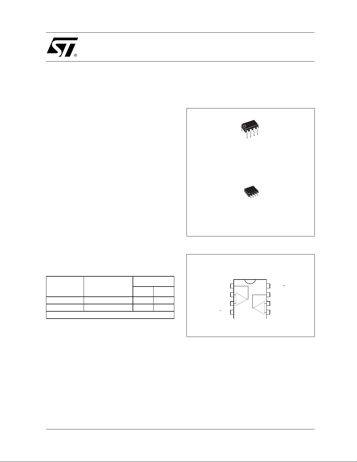
N
DIP8
(Plastic Package)
D
SO8
(Plastic Micropacka ge)
PIN CONNECTIONS (top view)
ORDER CODE
Part Number
MC33172 -40°C, +105°C
MC35172 -55°C, +125°C
Example : MC33172N
N = Dual in Line Package (DIP)
D = Small Outline Package (SO) - also available in Tape & Reel (DT))
November 2001
Temperature
Range
Package
ND
••
••
1/5
Page 2
MC33172-MC35172
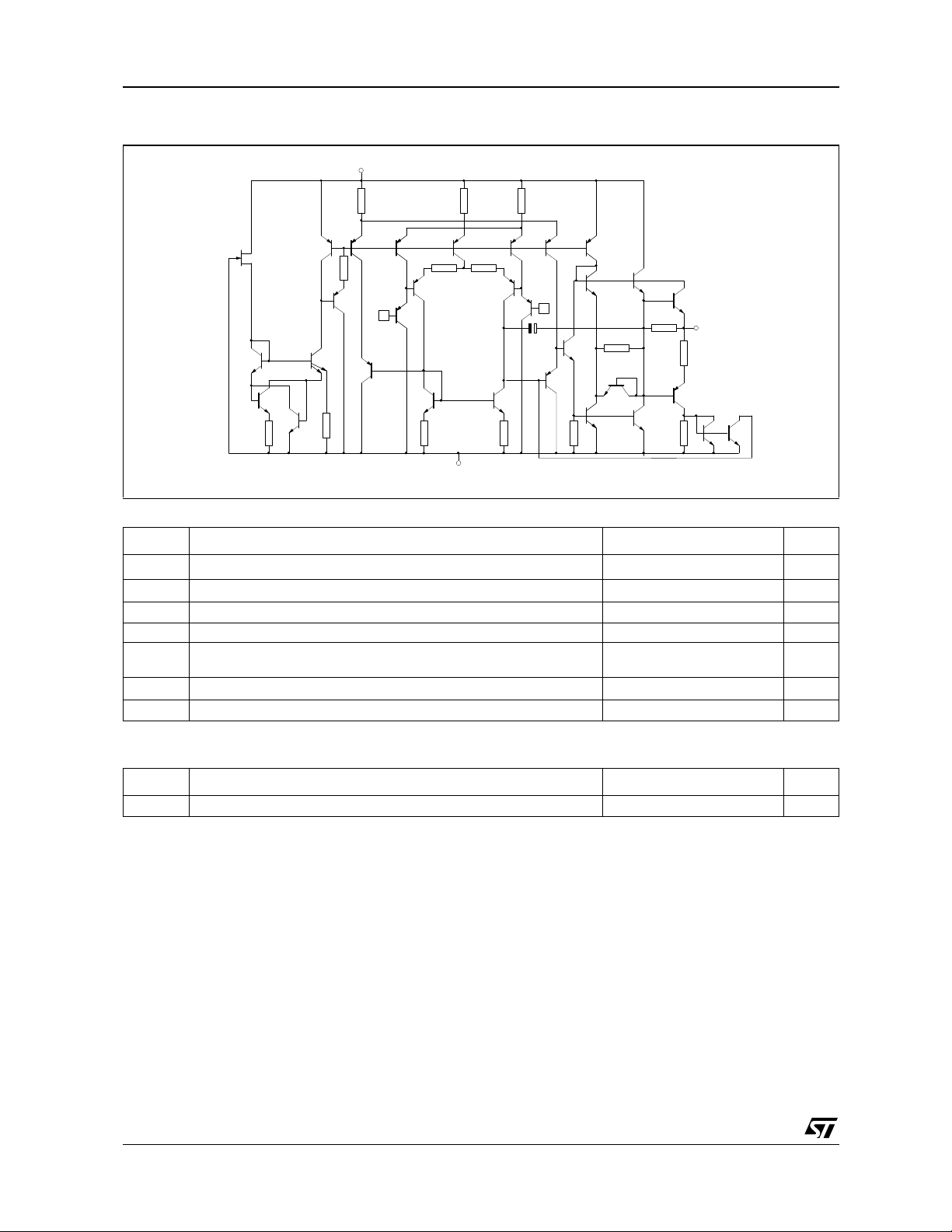
SCHEMATIC DIAGRAM (for 1/2MC33172)
V +
CC
R4
T8
T1
T2
T3
R1
T7
T5
T4
R2
T9
R3
T6
Input -
T14
T13
R5
R7
T15
T19
R9
V -
CC
R6
T13
T10
T11
R8
T16
T20
R10
T12
T25
Input +
T17
C
T21
T24
R12
T22
T27
T23
R11
T26
R13
Output
R14
T28
T29
R15
T30
T31
MAXIMUM RATINGS
Symbol Parameter Value Unit
V
T
T
1. Either or both input voltages must not exceed the magnitude of Vcc.
Supply Voltage ±22 V
CC
V
Differential Input Voltage
id
V
Input Voltage see note 1 V
i
see note
Output Short Circuit Duration Indefinite s
Operating Free-Air Temperature range MC33172
oper
MC35172
T
Junction Temperature 150 °C
j
Storage Temperature -65 to 150 °C
stg
-40 to 105
-55 to 125
1)
V
°C
OPERATING CONDITIONS
Symbol Parameter Value Unit
V
2/5
Supply Voltage ±2 to ±22 V
CC
Page 3

MC33172-MC35172
ELECTRICAL CHARACTERISTICS
+
V
= +15V, V
CC
Symbol Parameter Min. Typ. Max. Unit
Input Offset Voltage
V
io
V
V
V
DV
Input Offset Voltage Drift 10 µV/°C
io
Input Offset Current (Vic = 0V)
I
io
I
ib
A
vd
T
Input Bias Current (Vic = 0V)
T
Large Signal Voltage Gain (RL = 10kΩ, Vo = ±10V)
T
High Level Output Voltage
V
OH
V
V
V
Low Level Output Voltage
V
OL
V
V
V
Output Short Circuit Current (Vid = ±1V, Vo = 0V)
I
sc
V
CMR
SVR
Input Common Mode Voltage Range
icm
T
Common-mode Rejection Ratio (V
Supply Voltage Rejection Ratio (V
Supply Current
I
CC
V
V
V
Slew Rate (V
SR
GBP
Gain Bandwidth Product
Phase Margin (R
m
φ
e
Equivalent Input Noise Voltage (f = 1kHz) 29
n
THD Total Harmonic Distortion 0.05 %
V
O1/VO2
Channel Separation 120 dB
-
= -15V, RL connected to Ground, T
CC
+
= +15V, V
CC
+
= 5V, V
CC
+
= +15V, V
CC
. ≤ T
min
. ≤ T
min
. ≤ T
min
+
= 5V, V
CC
+
= +15V, V
CC
+
= +15V, V
CC
+
= 5V, V
CC
+
= +15V, V
CC
+
= +15V, V
CC
amb
amb
amb
-
= -15V, Vic = 0V
CC
-
= 0V, V
CC
-
CC
≤ T
max.
≤ T
max.
≤ T
max.
-
= 0V, RL = 10k
CC
-
CC
-
CC
-
= 0V, RL = 10k
CC
-
CC
-
CC
= 0V, Vo = 1.4V
ic
= -15V, Vic = 0V, T
= -15V, RL = 10k
= -15V, RL = 10kΩ, T
= -15V, RL = 10k
= -15V, RL = 10kΩ, T
Ω
Ω
Source
Sink
. ≤ T
min
+
CC
+
CC
+
CC
= 10kΩ, CL = 100pF, f = 100kHz
R
L
≤ T
amb
max
= 5V, V
= +15V, V
= +15V, V
-
= 0V, no load
CC
-
= -15V, no load
CC
-
= -15V no load, T
CC
= ±10V, RL = 10kΩ, CL = 100pF)
i
= 10kΩ, CL = 100pF)
L
ic
CC
≤ T
min.
amb
Ω
≤ T
min.
Ω
≤ T
min.
= V
icm min.
)
= ±5 to ±15V)
≤ T
min.
amb
= 25°C (unless otherwise specified)
amb
≤ T
max
.
50
25
3.5
13.6
amb
amb
≤ T
≤ T
max
max
.
.
13.3
3
15
-
V
CC
-
V
CC
to V
to (V
CC
CC
+
- 1.8)
+
- 2.2)
80 100 dB
80 100 dB
≤ T
max
.
1.6 2 V/µs
1.4 2.1
1
4.5
1
5
6.5
520
40
100
20
200
100
V/mV
4.2
14.2
0.1
0.15
-14
-13.6
-13.3
6
27
200
250
220
250
300
MHz
45 Degrees
----------- -
mV
nA
nA
V
V
mA
V
µ
nV
Hz
A
3/5
Page 4

MC33172-MC35172
PACKAGE MECHANICAL DATA
8 PINS - PLASTIC DIP
Dimensions
Min. Typ. Max. Min. Typ. Max.
A 3.32 0.131
a1 0.51 0.020
B 1.15 1.65 0.045 0.065
b 0.356 0.55 0.014 0.022
b1 0.204 0.304 0.008 0.012
D 10.92 0.430
E 7.95 9.75 0.313 0.384
e 2.54 0.100
e3 7.62 0.300
e4 7.62 0.300
F 6.6 0260
i 5.08 0.200
L 3.18 3.81 0.125 0.150
Z 1.52 0.060
Millimeters Inches
4/5
Page 5

PACKAGE MECHANICAL DATA
8 PINS - PLASTIC MICROPACKAGE (SO)
MC33172-MC35172
L
C
A
a2
b
e3
D
8
1
M
5
4
s
F
c1
a3
a1
E
b1
Millimeters Inches
Dimensions
Min. Typ. Max. Min. Typ. Max.
A 1.75 0.069
a1 0.1 0.25 0.004 0.010
a2 1.65 0.065
a3 0.65 0.85 0.026 0.033
b 0.35 0.48 0.014 0.019
b1 0.19 0.25 0.007 0.010
C 0.25 0.5 0.010 0.020
c1 45° (typ.)
D 4.8 5.0 0.189 0.197
E 5.8 6.2 0.228 0.244
e 1.27 0.050
e3 3.81 0.150
F 3.8 4.0 0.150 0.157
L 0.4 1.27 0.016 0.050
M 0.6 0.024
S 8° (max.)
Information furnished is bel ieved to be accurate and reliable. However, STMicroe lectronics assumes no responsibility for the
consequences of use of such information nor for any infringement of patents or other rights of third parties which may result from
its use. No li cense is granted by imp lica tion or otherwise under a ny patent or patent rig hts of STMicroelectronics. Spec ificat ions
mentioned in this publication ar e subject to change without notice. This publication supersedes and replaces all information
previously supplied. S TMicroelectronics products are not authorized for use as critica l components in life suppo rt devices or
systems without express written approval of STMicroelectronics.
Australi a - Brazil - Canada - Chin a - Finland - Fr ance - Germany - Hong Kong - India - Israel - I taly - Japan - Malaysia
Malta - Mor occo - Singapore - Spain - Sweden - Swit zerland - Uni ted Kingdom - United Sta te s
© The ST logo is a registered trademark of STMicroelectronics
© 2001 STM icroelectronics - Printed in Italy - All Rights Reserved
STMicr o el ectronics G ROU P OF COMPANIE S
© http://www.st.com
5/5
 Loading...