

Datasheet MC3503, MC3403D, MC3403N, MC3303N, MC3303D Datasheet (SGS Thomson Microelectronics)
...Page 1
MC3303
®
MC3403 - MC3503
LOW POWER QUAD BIPOLAR OPERATIONAL AMPLIFIERS
.SHORT-CIRCUIT PROTECTED OUTPUTS
.CLASS AB OUTPUT STAGE FOR MINIMAL
CROSSOVER DISTORTION
.SINGLE SUPPLY OPERATION : + 3 V TO + 36V
.DUAL SUPPLIES : ±1.5V TO ±18V
.LOW INPUT BIAS CU RRE N T : 500nA M A X
.INTERNALLY COMPENSATED
.SIMILAR PERFORMANCE TO POPULAR
UA741
DESCRIPTION
The MC3403 is a low-cos t, quad operation al amplifier with true differential inputs. The device has electrical characteristics similar to the popular UA741.
However the MC3403, has several distinct advantages over standard operational amplifier types in
single supply applications. The quad amplifier can
operate at sup ply v o l tages as low as 3. 0 v olt s or as
high as 36 volts with quiescent currents about one
third of those associated with the UA741 (on a per
amplifier basis ). The c ommon- mode inp ut range i ncludes the negative supply, thereby eliminating the
necessity for external biasing components in many
applications .
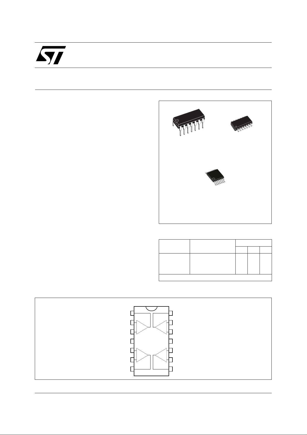
ORDER CODES
Part
Number
MC3303 –40
MC3403 0
MC3503 –55
Example : MC3403N
N
DIP14
(Plast ic Pac kag e)
(Thin Shrink Small Outline Package)
Temperature
o
(Plastic Micropackage)
P
TSSOP14
Range
o
C, +105oC •••
C, +70oC •••
o
C, +125oC •••
D
SO14
Package
NDP
PIN CONNECTIONS (top view)
Output 1
Inverting Input 1
Non-inverting Input 1
Non-inverting Input 2
Inverting Input 2
Output 2
August 1998
V
CC
1
2
-
+
3
+
4
5
+
-
6
7
14
Output 4
13
-
+
+
-
Inverting Input 4
12
Non-inverting Input 4
11
10
-
V
CC
Non-inverting Input 3
9
Inverting Input 3
8
Output 3
1/11
Page 2
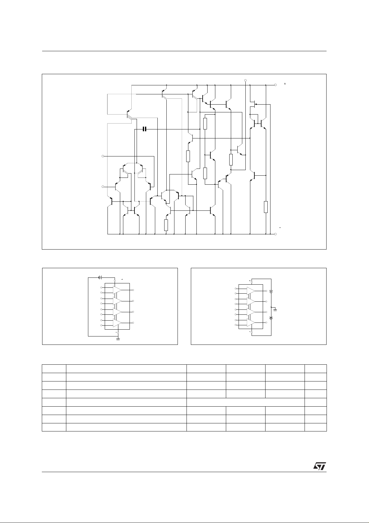
MC3303 - MC3 403 - MC35 03
SCHEMATIC DIAGRAM (each ampli fier)
Non-inverting
input
Inverting
input
(1 stage)
Q23
Q22 Q24
Q21
Q2
Q3
Output
Q19
Q20
C1
8pF
Q25
Q6
Q5
Q4
12k
Q7
Q14
R1
Ω
Q18
Q1
R6
Ω
0.7k
Q9
Q8
31k
37 k
Q17
Q16
R4
Ω
Q15
Q13
R2
Ω
Q12
Q11
Q10
Q27
Q28
R3
Ω
25
Q30
R5
8.2k
Ω
Q29
V
CC
(Ground)
V
CC
SINGL E SUP PLY
+3V to +30V
V
CC
V
CC
DUAL SUPPLIES
V
CC
1.5V to 18V
1.5V to 18V
V
CC
ABSOLUTE MAXIMUM RATINGS
Symbol Parameter MC3503 MC3403 MC3303 Unit
V
P
T
T
Notes : 1. For supply voltages less than ±15V , the abs ol ute maxi mum inpu t volt age is equal to the supply volt ag e.
Supply Voltage ±18 or 36 ±18 or 36 ±18 or 36 V
CC
Differential Input Voltage ±36 ±36 ±36 V
V
id
Input Voltage (note 1) ±18 ±18 ±18 V
V
i
– Output Short-circuit Duration (note 2) Infinite –
Power Dissipation 500 500 500 mW
tot
Operating Free-air Temperature Range –55 to +125 0 to +70 –40 to +105
oper
Storage Temperature Range –65 to +150 –65 to +150 –65 to +150
stg
2. Any of the amplifier outputs can be shorted to ground indefin itel y ; however more than one shou ld not be simultaneous ly short ed
as the maximum junc tio n te mpe rat ure wil l be excee d ed.
o
C
o
C
2/11
Page 3
ELECTRICAL CHARACTERISTICS
V
= ±15V, T
CC
Symbol Parameter
V
IO
I
IO
I
ib
A
vd
SVR Supply Voltage Rejection Ratio (R
I
CC
V
icm
CMR Common Mode Rejection Ratio (R
I
OS
± V
opp
SR Slew Rate (V
, t
t
r
f
K
OV
Z
I
Z
O
B
om
B Unity Gain Bandwidth (V
GBP Gain Bandwidth Product (V
THD Total Harmonic Distortion (f = 1kHz, A
e
n
= +25oC, (unless otherwise specified)
amb
Input Offset Voltage (RS ≤ 10kΩ)
T
= 25oC
amb
T
≤ T
amb
≤ T
max.
min.
Input Offset Current
= 25oC
T
amb
T
≤ T
amb
≤ T
max.
min.
Input Bias Current
T
= 25oC
amb
≤ T
T
min.
amb
≤ T
max.
Large Signal Voltage Gain (VO = ±10V, RL = 2kΩ)
T
= 25oC
amb
T
≤ T
amb
= 25oC
≤ T
amb
≤ T
≤ T
max.
max.
min.
T
amb
T
min.
Supply Current, all Amp, no Load
T
= 25oC
amb
≤ T
T
min.
amb
≤ T
max.
Input Common Mode Voltage Range
T
= 25oC
amb
≤ T
T
min.
T
amb
T
min.
amb
= 25oC
≤ T
amb
≤ T
≤ T
max.
max.
Output Short-circuit Current 10 30 45 mA
Output Voltage Swing
= 25oCR
T
amb
T
≤ T
min.
T
= 25oC, unity gain) 0.35 0.5
amb
≤ T
amb
max.
= ±10V RL = 2kΩ, CL = 100pF,
I
Rise Time and Fall T ime (VO = ± 20mV, RL = 2kΩ, CL = 100pF
T
= 25oC, unity gain) 0.18
amb
Overshoot (VI = ± 20mV, RL = 2kΩ, CL = 100pF,
= 25oC, unity gain) 10
T
amb
Input Impedance 0.3 1 MΩ
Output Impedance 75 Ω
Power Bandwidth (RL = 2kΩ, CL = 100pF, Av = 1, T
VO = 2Vpp, THD ≤ 5%) 9
= 10mV, RL = 2kΩ, CL = 100pF,
T
= 25oC, unity gain) 1
amb
f = 100kHz, T
= 25oC) 0.7 1
amb
VO = 2Vpp, CL = 100pF, T
O
= 10mV, RL = 2kΩ, CL = 100pF,
O
= 25oC) 0.02
amb
Equivalent Input Noise Voltage (f = 1kHz, Rs = 100Ω)43
≤ 10kΩ)
S
≤ 10kΩ)
S
= 20dB, RL = 2kΩ,
v
MC3303 - MC3 403 - MC35 03
Min. Typ. Max.
50
25
77
77
MC3503
MC3503
– 15
– 15
70
70
= 10kΩ
L
RL = 2kΩ
RL = 2kΩ
= 10kΩ
R
L
= 25oC,
amb
12
10
10
12
MC3303 - MC3403
MC3503
15
250
200
40 500
800
200
90
2.8 7
+ 13
+ 13
90
13.5
13
Unit
mV
6
nA
nA
V/mV
dB
mA
4
8
5
V
dB
V
V/µs
µs
%
kHz
MHz
MHz
%
nV
√Hz
3/11
Page 4
MC3303 - MC3 403 - MC35 03
ELECTRICAL CHARACTERISTICS (continued)
Symbol Parameter
∅m Phase Margin 60 Degrees
DV
DI
IO
V
O1/V02
ELECTRICAL CHARACTERISTICS
+
V
= 5V, V
CC
Input Offset Voltage Drift
IO
T
≤ T
amb
≤ T
max.
min.
Input Offset Current Drift
T
min
. ≤ T
≤ 25oC50
amb
Channel Separation 120 dB
–
= Ground, T
CC
= 25oC (unless otherwise specified)
amb
Symbol Parameter
V
IO
I
IO
I
ib
A
vd
SVR Supply Voltage Rejection Ratio (R
I
CC
V
opp
Input Offset Voltage (RS ≤ 10kΩ)
T
= 25 °C
amb
T
≤ T
amb
≤ T
max
min
Input Offset Current
T
= 25oC
amb
≤ T
T
min.
amb
≤ T
max.
Input Bias Current
T
= 25oC
amb
≤ T
T
min.
amb
≤ T
max.
Large Signal Voltage Gain (VO = 1.4 to 2.4V, RL = 2kΩ)
T
= 25oC
amb
T
≤ T
amb
= 25oC
≤ T
amb
≤ T
≤ T
max.
max.
≤ 10kΩ)
S
min.
T
amb
T
min.
Supply Current (All Amp)
MC3503
Output Voltage Range (RL = 10kΩ)
V
= +5V
CC
+5 < V
≤ +30V
CC
MC3303 - MC3403 - MC3503
Min. Typ. Max.
10
MC3303 - MC3403 - MC3503
Min. Typ. Max.
15
6
250
200
40 500
800
10
200
5
77
90
77
2.5 7
4
3.3
+
V
-2V
CC
3.5
+
V
-1.7V
CC
Unit
µV/oC
pA/oC
Unit
mV
nA
nA
V/mV
dB
mA
V
4/11
Page 5

CIRCUIT DESCRIPTION
The MC3403 is made using four inter nally compensated, two-stage operational amplifiers. The first
stage of each consists of differential input devices
Q24 and Q22 with input buffer transistors Q25 and
Q21 and the differential to single ended converter
Q3 and Q4. The first stage performs not only the first
stage gain function but also performs the level shifting and transconductance reduction functions. By
reducing the transconductance a smaller compensation capacitor (only 8pF) can be employed, thus
saving chi p are a.
The transconductance reduction is accomplished
by splitting the collectors of Q24 and Q22. Another
feature of thi s input st age is that th e in put co mmonmode range can include the negative supply of
TYPICAL PERFORMANCE CURVES
MC3303 - MC3 403 - MC35 03
ground, in single supply operation, without saturation eith er t he i nput devic es or th e d iffere ntial to si ngle-ended converter.
The second stage consists of a standard current
source load amplifier stage. The output stage is
unique because it allows the output to swing to
ground in single supply operation and yet does not
exhibit any crossover distortion in split supply operations. This is possible because class AB operation
is utilized.
Each amplifier is biased from an internal voltage
regulator which has a low temperature coefficient
thus givi ng each amplifier good temperatu re characteristics as w ell a s ex cel lent pow er su pply rej ection.
20µs/div.
APPLICATION INFORMATION
VOLTAGE REFERENCE
V
CC
R2
10kΩ
R1
10kΩ
V
O
=
R1 + R2
1
V
=
O
2
1/4
MC3403
R1
V
CC
V
CC
V
CC
AV = 100
WIEN BRI DGE OSCILL ATOR
50kΩ
5kΩ
V
V
O
(ref)
1
V
(ref)
=
2
10kΩ
V
CC
R
1/4
MC3403
C
V
CC
V
O
1
f
O
=
2 π RC
For
f
= 1kHz
O
C
R
R = 16kΩ
C = 0.01µF
5/11
Page 6

MC3303 - MC3 403 - MC35 03
APPLICATION INFORMATION (c ontin ued)
HIGH IMPEDANCE DIFFERENTIAL
AMPLIFIER
e
1
R1
e
2
1/4
MC3403
a R1
b R1
1/4
MC3403
1
R
C
1
R
C
R
1/4
MC3403
e
= C (1 + a + b) ( - )
o
R
BI-QUAD FILTER
COMPARATOR WI TH HYST ERESIS
R2
I
R1
R1
R1+ R2
R1
R1+ R2
R1
R1+ R2
MC3403
[ VOL−V
(ref)
[ VOH−V
[ VOH− VOL ]
1/4
(ref)
] + V
] + V
(ref)
(ref)
V
O
V
e
o
e
e
2
1
(ref)
V
VIL =
VIH =
H =
Hysteresis
V
OH
V
O
V
OL
V
V
I L
I H
V
(ref)
1
V
) =
V
R
(ref
R
(ref)
C
1/4
MC3403
Ω
100k
Ω
100k
1/4
MC3403
V
R3
(ref)
C1
e
I
R2
V
(ref)
C
1/4
MC3403
R
V
Bandpass output
fO =
R1 = QR
R2 =
R3 = TN R2
C1 = 10C
For : f
2
1
2Π RC
R1
T
BP
O
Q = 10
T
BP
TN = 1
CC
= 1kHz
= 1
R1
R2
Ω
R = 160k
µ
C = 0.001
R1 = 1.6M Ω
R2 = 1.6M Ω
R3 = 1.6M Ω
1/4
F
MC3403
Where T = Center frequency gain
V
(ref)
BP
T = Passband notch gain
N
C1
Notch output
6/11
Page 7

APPLICATION INFORMATION (c ontin ued)
FUNCTION GENERATOR
1
V
(ref)
V
=
CC
2
Triangle wave output
MC3303 - MC3 403 - MC35 03
R2
Ω
300k
V
(ref)
1/4
MC3403
C
R1 + R2
f =
4 CR R1
f
R3
75k
100k
V
(ref)
R
f
if R3 =
MULTIPLE FEEDBACK BANDPASS FILTER
C
R1
e
I
C
R2
Ω
R1
R3
Ω
R2 R1
R2 + R1
V
1/4
MC3403
CC
1/4
MC3403
Square wave output
e
o
C
O
= 10C
C
O
1
=
Q
C
πf
o
R3
2A ( f
R1 R5
2
4Q
V
CC
2
•
•
)
o
R1− R5•
V
(ref)
Given fo = Center frequency ; choose values fo, C then R3 =
) = Gain at center frequency R1 =
A (f
o
For less than 10% error from operational amplifier
Q
ofo
< 0.1 where fo and BW are expressed in Hz
BW
If source impedance varies, filter may be preceded with voltage follower buffer to stabilize filter parameters
V
(ref)
R2 =
7/11
Page 8

MC3303 - MC3 403 - MC35 03
TYPICAL PERFORMANCE CURVES
8/11
Page 9

PACKAGE MECHANICAL DATA
14 PINS - PLASTIC DIP
MC3303 - MC3 403 - MC35 03
Dimensions
Min. Typ. Max. Min. Typ. Max.
Millimeters Inches
a1 0.51 0.020
B 1.39 1.65 0.055 0.065
b 0.5 0.020
b1 0.25 0.010
D 20 0.787
E 8.5 0.335
e 2.54 0.100
e3 15.24 0.600
F 7.1 0.280
i 5.1 0.201
L 3.3 0.130
Z 1.27 2.54 0.050 0.100
PM-DIP14.EPS
DIP14.TBL
9/11
Page 10

MC3303 - MC3 403 - MC35 03
PACKAGE MECHANICAL DATA
14 PINS - PLASTIC MICROPACKAGE (SO)
Dimensions
Min. Typ. Max. Min. Typ. Max.
Millimeters Inches
A 1.75 0.069
a1 0.1 0.2 0.004 0.008
a2 1.6 0.063
b 0.35 0.46 0.014 0.018
b1 0.19 0.25 0.007 0.010
C 0.5 0.020
c1 45
o
(typ.)
D 8.55 8.75 0.336 0.334
E 5.8 6.2 0.228 0.244
e 1.27 0.050
e3 7.62 0.300
F 3.8 4.0 0.150 0.157
G 4.6 5.3 0.181 0.208
L 0.5 1.27 0.020 0.050
M 0.68 0.027
S8
o
(max.)
PM-SO14.EPS
SO14.TBL
10/11
Page 11

PACKAGE MECHANICAL DATA
14 PINS - THIN SHRINK SMALL OUTLINE PACKAGE
MC3303 - MC3 403 - MC35 03
Dim.
Min. Typ. Max. Min. Typ. Max.
Millimeters Inches
A 1.20 0.05
A1 0.05 0.15 0.01 0.006
A2 0.80 1.00 1.05 0.031 0.039 0.041
b 0.19 0.30 0.007 0.15
c 0.09 0.20 0.003 0.012
D 4.90 5.00 5.10 0.192 0.196 0.20
E 6.40 0.252
E1 4.30 4.40 4.50 0.169 0.173 0.177
e 0.65 0.025
k0
o
o
8
o
0
o
8
l 0.50 0.60 0.75 0.09 0.0236 0.030
Information furnished is believed to be accurate and reliable. However, STMicroelectronics assumes no responsibility for the
consequences of use of such information nor for any infringement of patents or other rights of third parties which may result
from its use. No license is granted by imp lication or otherwise under any patent or patent rights of STMicroelectronics. Specifications mentioned in this publication are subject to change without notice. This publication supersedes and replaces all information previously supplied. STMicroelectronics products are not authorized for use as critical components in life support
devices or systems without express written approval of STMicroelectronics.
© The ST logo is a trademark of STMicroelectronics
© 1998 STMicroelectronics – Printed in Italy – All Rights Reserved
STMicroelectronics GROUP OF COMPAN IES
Australia - Brazil - Canada - China - France - Germany - Italy - Japan - Korea - Malaysia - Malta - Mexico - Morocco
The Netherlands - Singapore - Spain - Sweden - Switzerland - Taiwan - Thailand - United Kingdom - U.S.A.
ORDER COD E :
11/11
 Loading...