

Page 1
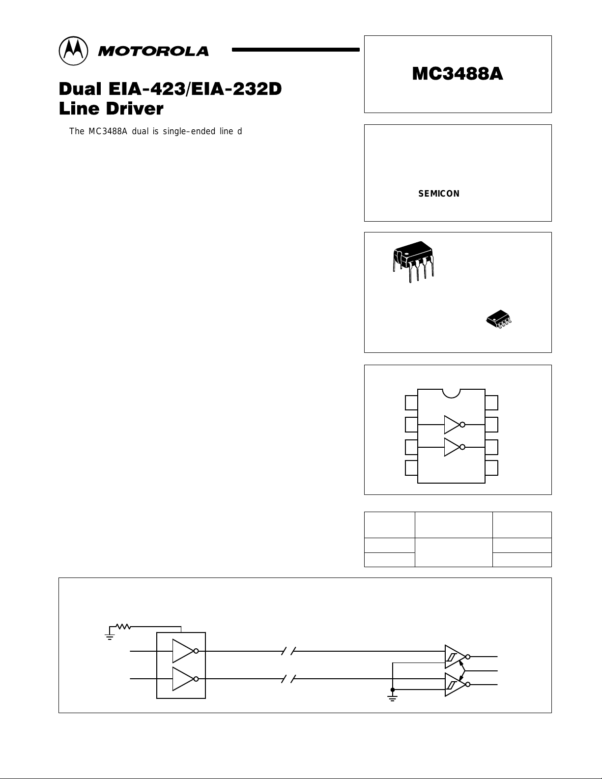
The MC3488A dual is single–ended line driver has been designed to
satisfy the requirements of EIA standards EIA–423 and EIA–232D, as well
as CCITT X.26, X.28 and Federal Standard FIDS1030. It is suitable for use
where signal wave shaping is desired and the output load resistance is
greater than 450 ohms. Output slew rates are adjustable from 1.0 µs to
100 µs by a single external resistor. Output level and slew rate are
insensitive to power supply variations. Input undershoot diodes limit
transients below ground and output current limiting is provided in both output
states.
The MC3488A has a standard 1.5 V input logic threshold for TTL or
NMOS compatibility .
• PNP Buffered Inputs to Minimize Input Loading
• Short Circuit Protection
• Adjustable Slew Rate Limiting
• MC3488A Equivalent to 9636A
• Output Levels and Slew Rates are Insensitive to Power
Supply Voltages
• No External Blocking Diode Required for V
• Second Source µA9636A
EE
Supply
Order this document by MC3488A/D
DUAL
EIA–423/EIA–232D
DRIVER
SEMICONDUCTOR
TECHNICAL DATA
P1 SUFFIX
PLASTIC PACKAGE
CASE 626
D SUFFIX
PLASTIC PACKAGE
CASE 751
(SO–8)
Wave Shape
Control
Simplified Application
MC3488A Driver
RS–423 Interface
Wave
Shape
Input A
Input B
Gnd
ORDERING INFORMATION
Device
MC3488AP1
MC3488AD
PIN CONNECTIONS
1
2
3
4
Operating
Temperature Range
TA = 0 to +70°C
MC3486
Three–State Receiver
V
8
CC
7
Output A
6
Output B
5
V
EE
Plastic DIP
Package
SO–8
TTL Logic
MOTOROLA ANALOG IC DEVICE DATA
Motorola, Inc. 1996 Rev 2
1
Page 2
MC3488A
MAXIMUM RATINGS (Note 1)
Rating Symbol Value Unit
Power Supply Voltages V
Output Current
Source
Sink
Operating Ambient Temperature T
Junction Temperature Range T
Storage Temperature Range T
V
I
O+
I
O–
CC
EE
A
J
stg
RECOMMENDED OPERATING CONDITIONS
Characteristic Symbol Min Typ Max Unit
Power Supply Voltages V
Operating Temperature Range T
Wave Shaping Resistor R
TARGET ELECTRICAL CHARACTERISTICS (Unless otherwise noted, specifications apply over recommended operating conditions)
Characteristic
Input Voltage – Low Logic State V
Input Voltage – High Logic State V
Input Current – Low Logic State
(VIL = 0.4 V)
Input Current – High Logic State
(VIH = 2.4 V)
(VIH = 5.5 V)
Input Clamp Diode Voltage
(IIK = – 15 mA)
Output Voltage – Low Logic State
(RL = ∞) EIA–423
(RL= 3.0 kΩ) EIA–232D
(RL= 450 Ω) EIA–423
Output Voltage – High Logic State
(RL = ∞) EIA–423
(RL.= 3.0 kΩ) EIA–232D
(RL = 450 Ω) EIA–423
Output Resistance
(RL q 450 Ω)
Output Short–Circuit Current (Note 2)
(Vin = V
(Vin = V
Output Leakage Current (Note 3)
(VCC = VEE = 0 V, – 6.0 V p Vop
Power Supply Currents
(RW = 100 kΩ, RL = ∞, VIL p Vinp
NOTES: 1. Devices should not be operated at these values. The IElectrical CharacteristicsI provide conditions for actual device operation.
= 0 V)
out
, V
IH(Min)
2.One output shorted at a time.
3.No VEE diode required.
out
= 0 V)
6.0 V)
VIH)
+ 15
– 15
+ 150
– 150
0 to + 70 °C
150 °C
– 65 to + 150 °C
CC
V
EE
A
WS
10.8
– 13.2
0 25 70 °C
10 – 1000 kΩ
Symbol Min Typ Max Unit
IL
IH
I
IL
I
IH1
I
IH2
V
IK
V
OL
V
OH
R
O
I
OSH
I
OSL
I
ox
I
CC
I
EE
V
mA
12
–12
– – 0.8 V
2.0 – – V
– 80 – – µA
–
–
– 1.5 – – V
– 6.0
– 6.0
– 6.0
5.0
5.0
4.0
– 25 50 Ω
– 150
+15
– 100 – 100 µA
–
–18
–
–
–
–
–
–
–
–
–
–
–
–
13.2
– 10.8
10
100
– 5.0
– 5.0
– 4.0
6.0
6.0
6.0
– 15
+ 150
+ 18
–
V
µA
V
V
mA
mA
2
MOTOROLA ANALOG IC DEVICE DATA
Page 3

MC3488A
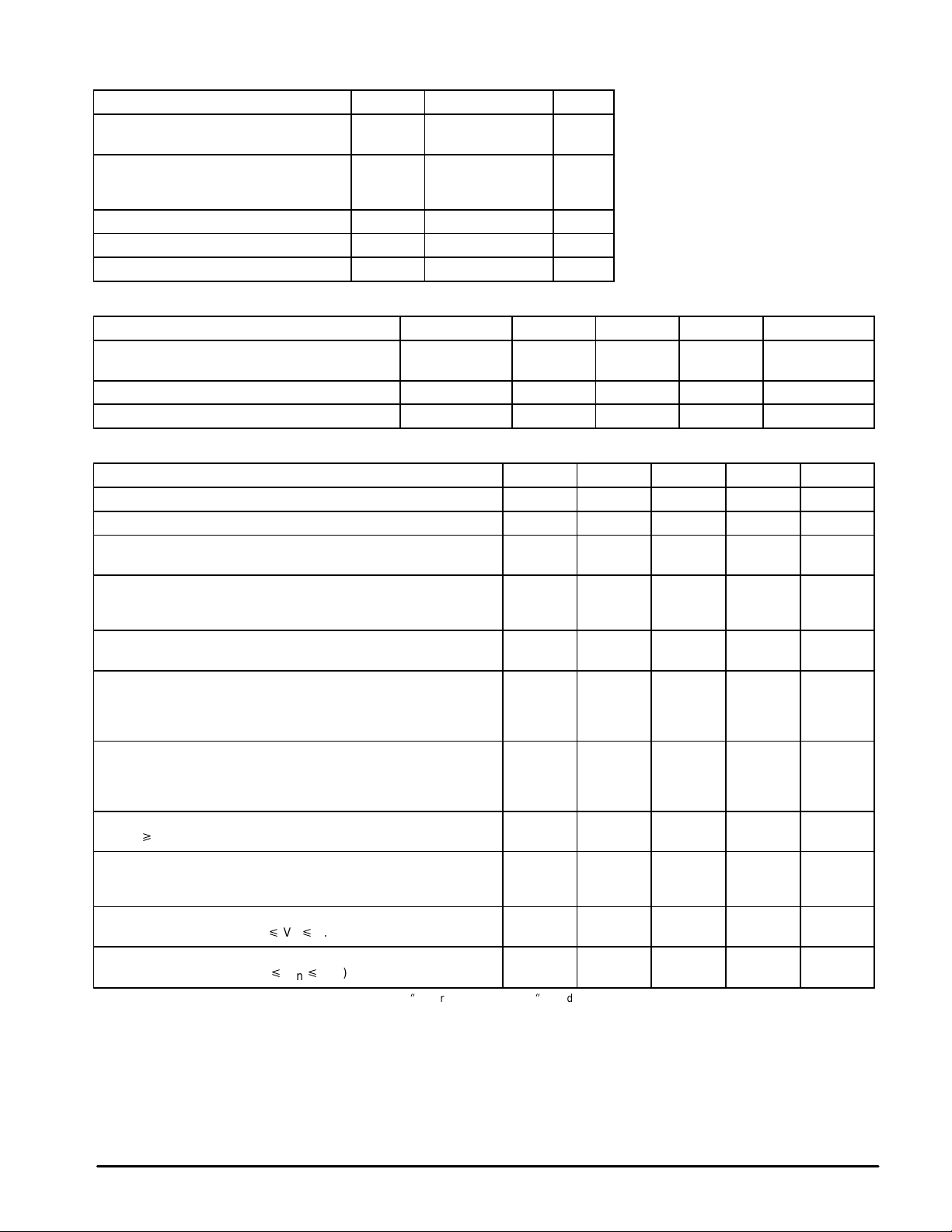
TRANSITION TIMES (Unless otherwise noted, C
Transition times measured 10% to 90% and 90% to 10%)
Characteristic
Transition Time, Low–to–High State Output
(RW = 10 kΩ)
(RW = 100 kΩ)
(RW = 500 kΩ)
(RW = 1000 kΩ)
Transition Time, High–to–Low State Output
(RW = 10 kΩ)
(RW = 100 kΩ)
(RW = 500 kΩ)
(RW = 1000 kΩ)
= 30 pF, f = 1.0 kHz, VCC = – VEE = 12.0 V ± 10%, TA = 25°C, RL = 450 Ω.
L
Symbol Min Typ Max Unit
Figure 1. Test Circuit and Waveforms
To
Scope
(Input)
Pulse
Generator
f = 1.0 kHz
PW = 500
µ
s
50
R
t
TLH
t
THL
0.8
8.0
40
80
0.8
8.0
40
80
for Transition Times
V
CC
MC3488A
WS
R
L
–
–
–
–
–
–
–
–
To
Scope
(Output)
C
(Includes
Probe and Jig
Capacitance)
1.4
µs
14
70
140
µs
1.4
14
70
140
L
3.0 V
Input
0 V
V
OH
0 V
Output
V
OL
t
THL
90%
V
EE
10%10%
Note: Input Rise
and Fall Times
to
90%) p 10 ns
(10%
90%
t
TLH
MOTOROLA ANALOG IC DEVICE DATA
3
Page 4

MC3488A
Figure 2. Output Transition Times versus
Wave Shape Resistor Value
1000
Ω
w
100
CL = 30 pF
10
WAVE SHAPE RESISTOR, R (k )
1.0
0.1 0
TRANSITION TIMES, t
TLH/tTHL
(µs)
1000100101.0
Figure 4. Output Current versus Output Voltage
Power–On Power–Off
50
40
Vin = V
IH(Min)
TA = 25°C
VCC = 12 V
VEE = –12 V
RWS = 100 k
Vin = 0 V
Ω
6.0– 6.0 10
10– 2.0 0 2.0 4.0– 8.0
–10
–20
, OUTPUT CURRENT (mA)
–30
out
I
–40
–50
30
20
10
0
–10
– 4.0 8.0 – 6.0 6.0
V
, OUTPUT VOLTAGE (V)
out
– 2.0
, OUTPUT VOL TAGE (V)
out
– 4.0
V
– 6.0
– 0.02
– 0.04
, OUTPUT CURRENT (mA)
out
– 0.06
I
– 0.08
– 0.10
6.0
4.0
2.0
0
0.10
0.08
0.06
0.04
0.02
0
Figure 3. Input/Output Characteristics
versus T emperature
0°C
TA = 25°C
70°C
VCC = 12 V
VEE = –12 V
RWS = 100 k
RL = 450
– 8.0 4.02.00– 2.0 108.0– 4.0
Ω
Ω
1.0
Vin, INPUT VOLTAGE (V)
VCC = VEE = Vin = 0 V
°
C
TA = 25
(No diode required
at VEE Pin.)
V
, OUTPUT VOLTAGE (V)
out
2.0
12.0
10.0
– 2.0
– 4.0
– 6.0
, SUPPLY CURRENT (mA)I
– 8.0
xx
– 10.0
– 12.0
4
Figure 5. Supply Current versus T emperature Figure 6. Rise/Fall Time versus R
100
1
VCC = 12 V
VEE = – 12 V
CL = 30 pF
TA = 0°C, 70°C
TA = 25°C
100 k
RWS, WA VE SHAPING RESISTANCE (
8.0
6.0
4.0
2.0
Vin = 0 V, Vin = V
VCC = 12V
VEE = – 12 V
0
RWS = 100 k
3010 40 50
20
TA, AMBIENT TEMPERATURE (
Ω
Vin = 0 V
Vin = V
IH
IH
, RL =
∞
60 70
I
CC
I
EE
90 100
800
°
C)
µ
, RISE/FALL TIME ( s)t
THL
TLH
t
10
MOTOROLA ANALOG IC DEVICE DATA
WS
Ω
)
1M10 k
Page 5

MC3488A
OUTLINE DIMENSIONS
P1 SUFFIX
PLASTIC PACKAGE
CASE 626–05
ISSUE K
NOTE 2
–T–
SEATING
PLANE
H
–T–
58
–B–
14
F
–A–
C
N
D
G
0.13 (0.005) B
–A–
58
4X P
–B–
14
G
C
SEATING
PLANE
8X D
K
SS
K
M
M
A
T
0.25 (0.010)MB
A0.25 (0.010)MTB
L
J
M
M
D SUFFIX
PLASTIC PACKAGE
CASE 751–05
(SO–8)
ISSUE N
M
R
X 45
_
_
M
NOTES:
1. DIMENSION L TO CENTER OF LEAD WHEN
FORMED PARALLEL.
2. PACKAGE CONTOUR OPTIONAL (ROUND OR
SQUARE CORNERS).
3. DIMENSIONING AND TOLERANCING PER ANSI
Y14.5M, 1982.
DIM MIN MAX MIN MAX
A 9.40 10.16 0.370 0.400
B 6.10 6.60 0.240 0.260
C 3.94 4.45 0.155 0.175
D 0.38 0.51 0.015 0.020
F 1.02 1.78 0.040 0.070
G 2.54 BSC 0.100 BSC
H 0.76 1.27 0.030 0.050
J 0.20 0.30 0.008 0.012
K 2.92 3.43 0.115 0.135
L 7.62 BSC 0.300 BSC
M ––– 10 ––– 10
N 0.76 1.01 0.030 0.040
NOTES:
1. DIMENSIONING AND TOLERANCING PER
ANSI Y14.5M, 1982.
2. CONTROLLING DIMENSION: MILLIMETER.
3. DIMENSIONS A AND B DO NOT INCLUDE
MOLD PROTRUSION.
4. MAXIMUM MOLD PROTRUSION 0.15 (0.006)
PER SIDE.
5. DIMENSION D DOES NOT INCLUDE DAMBAR
PROTRUSION. ALLOWABLE DAMBAR
PROTRUSION SHALL BE 0.127 (0.005) TOTAL
IN EXCESS OF THE D DIMENSION AT
MAXIMUM MATERIAL CONDITION.
DIM MIN MAX MIN MAX
F
J
A 4.80 5.00 0.189 0.196
B 3.80 4.00 0.150 0.157
C 1.35 1.75 0.054 0.068
D 0.35 0.49 0.014 0.019
F 0.40 1.25 0.016 0.049
G 1.27 BSC 0.050 BSC
J 0.18 0.25 0.007 0.009
K 0.10 0.25 0.004 0.009
M 0 7 0 7
P 5.80 6.20 0.229 0.244
R 0.25 0.50 0.010 0.019
INCHESMILLIMETERS
__
INCHESMILLIMETERS
____
MOTOROLA ANALOG IC DEVICE DATA
5
Page 6

MC3488A
Motorola reserves the right to make changes without further notice to any products herein. Motorola makes no warranty , representation or guarantee regarding
the suitability of its products for any particular purpose, nor does Motorola assume any liability arising out of the application or use of any product or circuit, and
specifically disclaims any and all liability, including without limitation consequential or incidental damages. “T ypical” parameters which may be provided in Motorola
data sheets and/or specifications can and do vary in different applications and actual performance may vary over time. All operating parameters, including “Typicals”
must be validated for each customer application by customer’s technical experts. Motorola does not convey any license under its patent rights nor the rights of
others. Motorola products are not designed, intended, or authorized for use as components in systems intended for surgical implant into the body, or other
applications intended to support or sustain life, or for any other application in which the failure of the Motorola product could create a situation where personal injury
or death may occur. Should Buyer purchase or use Motorola products for any such unintended or unauthorized application, Buyer shall indemnify and hold Motorola
and its officers, employees, subsidiaries, affiliates, and distributors harmless against all claims, costs, damages, and expenses, and reasonable attorney fees
arising out of, directly or indirectly, any claim of personal injury or death associated with such unintended or unauthorized use, even if such claim alleges that
Motorola was negligent regarding the design or manufacture of the part. Motorola and are registered trademarks of Motorola, Inc. Motorola, Inc. is an Equal
Opportunity/Affirmative Action Employer.
How to reach us:
USA/EUROPE/Locations Not Listed: Motorola Literature Distribution; JAPAN: Nippon Motorola Ltd.; Tatsumi–SPD–JLDC, 6F Seibu–Butsuryu–Center,
P.O. Box 20912; Phoenix, Arizona 85036. 1–800–441–2447 or 602–303–5454 3–14–2 T atsumi Koto–Ku, Tokyo 135, Japan. 03–81–3521–8315
MFAX: RMF AX0@email.sps.mot.com – TOUCHT ONE 602–244–6609 ASIA/PACIFIC: Motorola Semiconductors H.K. Ltd.; 8B Tai Ping Industrial Park,
INTERNET: http://Design–NET.com 51 Ting Kok Road, Tai Po, N.T., Hong Kong. 852–26629298
6
◊
MOTOROLA ANALOG IC DEVICE DATA
MC3488A/D
*MC3488A/D*
 Loading...