

Page 1
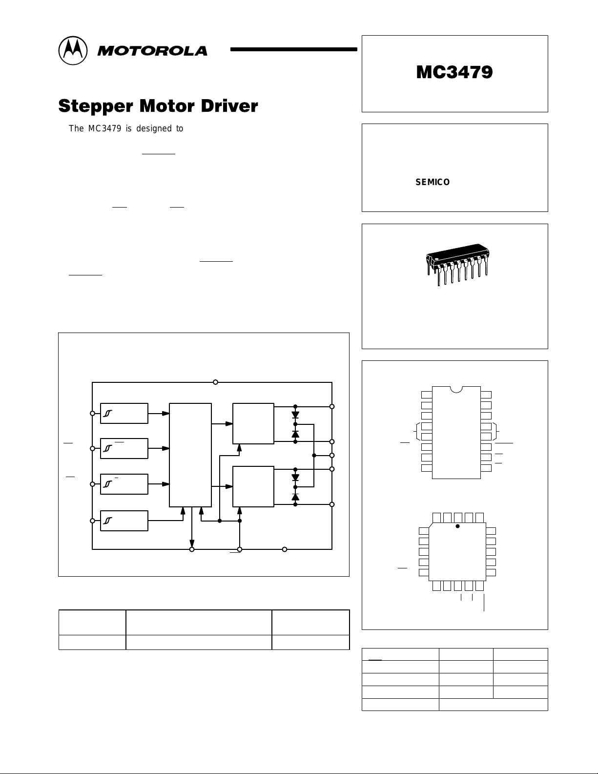
The MC3479 is designed to drive a two–phase stepper motor in the
bipolar mode. The circuit consists of four input sections, a logic
decoding/sequencing section, two driver–stages for the motor coils, and an
output to indicate the Phase A
• Single Supply Operation: 7.2 to 16.5 V
• 350 mA/Coil Drive Capability
• Clamp Diodes Provided for Back–EMF Suppression
• Selectable CW/CCW and Full/Half Step Operation
• Selectable High/Low Output Impedance (Half Step Mode)
• TTL/CMOS Compatible Inputs
• Input Hysteresis: 400 mV Minimum
• Phase Logic Can Be Initialized to Phase A
• Phase A Output Drive State Indication (Open–Collector)
• Available in Standard DIP and Surface Mount
drive state.
Order this document by MC3479/D
STEPPER MOTOR
DRIVER
SEMICONDUCTOR
TECHNICAL DATA
P SUFFIX
PLASTIC PACKAGE
CASE 648C
Figure 1. Representative Block Diagram
V
M
Clock
CW/CCW
/H Step
F
OIC
Logic
/SetPhase A
Driver
Driver
GndBias
CW
Full
Step
Clk
/CCW
/Half
OIC
ORDERING INFORMATION
Operating
Device
MC3479P TA = 0° to +70°C Plastic
Temperature Range
Package
PIN CONNECTIONS
V
V
L3
M
D
20
11 12 13
Full/Half Step
Phase A
CW/CCW
16
15
14
13
12
11
10
9
V
L3
L4
Phase A
CW/CCW
Ful
Step
17
16
15
148
M
Gnd
l/Half
L4
Gnd
Gnd
Gnd
Gnd
1
V
D
2
L1
L2
V
D
L3
L4
L2
3
L1
4
Gnd
5
6
Bias
/Set
Clk
7
8
OIC
(Top View)
L2
L1
21519
3
418
Gnd
Gnd
6
Gnd
7
Gnd
Bias/Set
10
9
Clk
OIC
INPUT TRUTH TABLE
Input Low Input High
CW
/CCW
/Half Step
Full
OIC
CW CCW
Full Step Half Step
Hi Z Low Z
Positive Edge TriggeredClk
MOTOROLA ANALOG IC DEVICE DATA
Motorola, Inc. 1996 Rev 1
1
Page 2
MC3479
MAXIMUM RATINGS
Rating Symbol Value Unit
Supply Voltage V
Clamp Diode Cathode Voltage (Pin 1) V
Driver Output Voltage V
Drive Output Current/Coil I
Input Voltage (Logic Controls) V
Bias/Set Current I
Phase A Output Voltage V
Phase A Sink Current I
Junction Temperature T
Storage Temperature Range T
M
D
OD
OD
in
BS
OA
OA
J
stg
RECOMMENDED OPERATING CONDITIONS
Characteristic Symbol Min Max Unit
Supply Voltage V
Clamp Diode Cathode Voltage V
Driver Output Current (Per Coil) (Note 1) I
Input Voltage (Logic Controls) V
Bias/Set Current (Outputs Active) I
Phase A Output Voltage V
Phase A Sink Current I
Operating Ambient Temperature T
NOTE: 1. See section on Power Dissipation in Application Information.
+ 18 Vdc
VM + 5.0 Vdc
VM + 6.0 Vdc
± 500 mA
– 0.5 to + 7.0 Vdc
– 10 mA
+ 18 Vdc
20 mA
+ 150 °C
– 65 to + 150 °C
OD
BS
OA
OA
M
D
+ 7.2 + 16.5 Vdc
V
M
VM + 4.5 Vdc
— 350 mA
in
0 + 5.5 Vdc
– 300 – 75 µA
— V
M
Vdc
0 8.0 mA
A
0 + 70 °C
DC ELECTRICAL CHARACTERISTICS (Specifications apply over the recommended supply voltage and temperature range, [Notes
2, 3] unless otherwise noted.)
Characteristic
INPUT LOGIC LEVELS
Threshold Voltage (Low–to–High)
Threshold Voltage (High–to–Low)
Hysteresis V
Current: (VI = 0.4 V)
Current: (VI = 5.5 V)
Current: (VI = 2.7 V)
DRIVER OUTPUT LEVELS
Output High Voltage 2, 3, V
(IBS = – 300 µA): (IOD = – 350 mA)
(IBS = – 300 µA): (IOD = – 0.1 mA)
Output Low Voltage V
(IBS = – 300 µA, IOD = 350 mA)
Differential Mode Output Voltage Difference (Note 4) DV
(IBS = – 300 µA, IOD = 350 mA)
Common Mode Output Voltage Dif ference (Note 5) CV
(IBS = – 300 µA, IOD = – 0.1 mA)
Output Leakage, Hi Z State µA
(0 p VOD p VM, IBS = – 5.0 µA) I
(0 p VOD p VM, IBS = – 300 µA, F/H = 2.0 V, OIC = 0.8 V) I
NOTES: 2. Algebraic convention rather than absolute values is used to designate limit values.
3.Current into a pin is designated as positive. Current out of a pin is designated as negative.
4.DVOD = V
5.CVOD = V
OD1,2
OHD1
– V
– V
OD3,4
OHD2
where: V
or V
OHD3
OD1,2
V
OD3,4
– V
= (V
OHD4
OHD1
= (V
.
– V
OHD3
OLD2
– V
) or (V
OLD4
Pins Symbol Min Typ Max Unit
7, 8,
9, 10
V
V
TLH
THL
HYS
I
IL
— — 2.0 Vdc
0.8 — — Vdc
0.4 — — Vdc
–100
—
—
—
—
+100
—
+20
OHD
14, 15 VM – 2.0
VM – 1.2——
— — 0.8 Vdc
— — 0.15 Vdc
— — 0.15 Vdc
– 100 — + 100
– 100 — + 100
OHD2
) or (V
– V
OHD4
OLD1
– V
), and
OLD3
OLD
OD
OD
OZ1
OZ2
).
—
µA
Vdc
—
—
2
MOTOROLA ANALOG IC DEVICE DATA
Page 3
MC3479
DC ELECTRICAL CHARACTERISTICS (Specifications apply over the recommended supply voltage and temperature range, [Notes
2, 3] unless otherwise noted.)
Characteristic
CLAMP DIODES
Forward Voltage 1, 2, 3, V
(ID = 350 mA) 14, 15
Leakage Current (Per Diode) I
(Pin 1 = 21 V; Outputs = 0 V; IBS = 0 µA)
PHASE A OUTPUT
Output Low Voltage 11 V
(IOA = 8.0 mA)
Off State Leakage Current I
(V
= 16.5 V)
OHA
POWER SUPPLY
Power Supply Current 16 mA
(IOD = 0 µA, IBS = – 300 µA)
(L1 = V
(L1 = V
(L1 = V
BIAS/SET CURRENT
To Set Phase A 6 I
OHD
OHD
OHD
, L2 = V
, L2 = V
, L2 = V
, L3 = V
OLD
, L3 = Hi Z, L4 = Hi Z) I
OLD
, L3 = V
OLD
OHD
OHD
, L4 = V
, L4 = V
) I
OLD
) I
OHD
Pins Symbol Min Typ Max Unit
DF
DR
OLA
OHA
MW
MZ
MN
BS
— 2.5 3.0 Vdc
— — 100 µA
— — 0.4 Vdc
— — 100 µA
— — 70
— — 40
— — 75
– 5.0 — — µA
PACKAGE THERMAL CHARACTERISTICS
Characteristic Symbol Min Typ Max Unit
Thermal Resistance, Junction–to–Ambient (No Heatsink) R
AC SWITCHING CHARACTERISTICS (T
Characteristic
Clock Frequency 7 f
Clock Pulse Width (High) 7 PW
Clock Pulse Width (Low) 7 PW
Bias/Set Pulse Width 6 PW
Setup Time (CW/CCW and F/HS) 10–7
Hold Time (CW/CCW and F/HS) 10–7
Propagation Delay (Clk–to–Driver Output) t
Propagation Delay (Bias/Set–to–Driver Output) t
Propagation Delay (Clk–to–Phase A Low) 7–11 t
Propagation Delay (Clk–to–Phase A High) 7–11 t
NOTES: 2. Algebraic convention rather than absolute values is used to designate limit values.
3.Current into a pin is designated as positive. Current out of a pin is designated as negative.
= + 25°C, VM = 12 V) (See Figures 2, 3, 4)
A
Pins Symbol Min Typ Max Unit
9–7
9–7
θJA
CK
CKH
CKL
BS
t
su
t
h
PCD
PBSD
PHLA
PLHA
— 45 — °C/W
0 — 50 kHz
10 — — µs
10 — — µs
10 — — µs
5.0 — — µs
10 — — µs
— 8.0 — µs
— 1.0 — µs
— 12 — µs
— 5.0 — µs
MOTOROLA ANALOG IC DEVICE DATA
3
Page 4

MC3479
CW
Bias
F / HS
/ CCW
Figure 2. AC Test Circuit
+ 12 V
/Set
Clk
OIC
56 k
6
MC3479P
7
8
9
10
41213
0.1
µ
F
V
M
16
2
3
14
15
5
1.0 k
L2
1.0 k
L1
1.0 k
1.0 k
L4
1.0 k
L3
1.0 k
11
4.0 k
+ 12 V
Phase A
Bias/Set
Input
L1 – L4
Outputs
V
M
0
Figure 3. Bias/Set Timing
(Refer to Figure 2)
PW
BS
VM – 1.0 VM – 1.0
t
PBSD
(High Impedance)
Note: tr, tf (10% to 90%) for
input signals are
p
25 ns.
t
PBSD
PIN FUNCTION DESCRIPTION
Pin No.
20–Pin 16–Pin
20 16 Power Supply V
4, 5, 6, 7,
14, 15, 16, 17
4, 5,
12, 13
1 1 Clamp Diode
2, 3,
18, 19
2, 3,
14, 15
8 6 Bias/Set B/S This pin is typically 0.7 volts below VM. The current out of this pin
9 7 Clock Clk The positive edge of the clock input switches the outputs to the next
11 9 Full/Half Step F/HS When low (Logic “0”), each clock input pulse will cause the motor to
12 10 Clockwise/
10 8 Output Impedance
13 11 Phase A Ph A This open–collector output indicates (when low) that the driver outputs
Function Symbol Description
M
Power supply pin for both the logic circuit and the motor coil current.
Voltage range is + 7.2 to + 16.5 volts.
Ground Gnd Ground pins for the logic circuit and the motor coil current. The
physical configuration of the pins aids in dissipating heat from within
the IC package.
Voltage
V
D
This pin is used to protect the outputs where large voltage spikes may
occur as the motor coils are switched. Typically a diode is connected
between this pin and Pin 16. See Figure 11.
Driver Outputs L1, L2
L3, L4
High current outputs for the motor coils. L1 and L2 are connected to
one coil, and L3 and L4 to the other coil.
(through a resistor to ground) determines the maximum output sink
current. If the pin is opened (IBS < 5.0 µA) the outputs assume a high
impedance condition, while the internal logic presets to a Phase A
condition.
position. This input has no effect if Pin 6 is open.
rotate one full step. When high, each clock pulse will cause the motor
to rotate one–half step. See Figure 7 for sequence.
CW/CCW This input allows reversing the rotation of the motor. See Figure 7 for
Counterclockwise
sequence.
OIC This input is relevant only in the half step mode (Pin 9 > 2.0 V). When
Control
low (Logic “0”), the two driver outputs of the non–energized coil will be
in a high impedance condition. When high the same driver outputs will
be at a low impedance referenced to VM. See Figure 7.
are in the Phase A
condition (L1 = L3 = V
, L2 = L4 = V
OHD
OLD
).
APPLICATION INFORMATION
General
The MC3479 integrated circuit is designed to drive a
stepper positioning motor in applications such as disk drives
and robotics. The outputs can provide up to 350 mA to each
of two coils of a two–phase motor. The outputs change state
with each low–to–high transition of the clock input, with the
new output state depending on the previous state, as well as
the input conditions at the logic controls.
4
Outputs
The outputs (L1–L4) are high current outputs (see
Figure 5), which when connected to a two–phase motor,
provide two full–bridge configurations (L3 and L4 are not
shown in Figure 5). The polarities applied to the motor coils
depend on which transistor (QH or QL) of each output is on,
which in turn depends on the inputs and the decoding
circuitry.
MOTOROLA ANALOG IC DEVICE DATA
Page 5

MC3479
Figure 4. Clock Timing
(Refer to Figure 2)
Clk
F
/HS,
/CCW
CW
Inputs
Phase A
Output
B
/S
3.0 V
0
L1 – L4
Outputs
0
3.0 V
1.5 V
t
PCD
PW
I
′
BS
CLKH
6.0 V
PW
CLKL
tht
su
1.5 V
t
PHLA
1.5 V
Figure 5. Output Stages
V
M
Q
H
Q
L
L1
t
PLHA
Motor Coil
Note: tr, tf (10% to 90%) for input
p
signals are
V
D
L2
10 ns.
Q
H
Q
L
I
BS
R
B
Current
Drivers
and
Logic
To L3, L4
Transistors
CW
/ CCW
The maximum sink current available at the outputs is a
function of the resistor connected between Pin 6 and ground
(see section on Bias
/Set operation). Whenever the outputs
are to be in a high impedance state, both transistors (QH and
QL of Figure 5) of each output are off.
V
D
This pin allows for provision of a current path for the motor
coil current during switching, in order to suppress back–EMF
voltage spikes. VD is normally connected to VM (Pin 16)
through a diode (zener or regular), a resistor, or directly. The
peaks instantaneous voltage at the outputs must not exceed
VM by more than 6.0 V. The voltage drop across the internal
clamping diodes must be included in this portion of the design
(see Figure 6). Note the parasitic diodes (Figure 5) across
each QL of each output provide for a complete circuit path for
the switched current.
Logic Decoding
Circuit
/HS
Inputs
3.0
2.0
F
V (V)
1.0
Parasitic
Diodes
OIC
ClkF
Figure 6. Clamp Diode Characteristics
0
ID (mA)
300100 2000
MOTOROLA ANALOG IC DEVICE DATA
5
Page 6

MC3479
Full
/Half Step
When this input is at a Logic “0” (<0.8 V), the outputs
change a full step with each clock cycle, with the sequence
direction depending on the CW
steps (Phase A
, B, C, D) for each complete cycle of the
sequencing logic. Current flows through both motor coils
during each step, as shown in Figure 7.
When taken to a Logic “1” (>2.0 V), the outputs change a
half step with each clock cycle, with the sequence direction
depending on the CW
/CCW input. Eight steps (Phase A to H)
result for each complete cycle of the sequenc ing logic. Phas e
A, C, E and G correspond (in polarity) to Phase A, B, C, and
D
, respectively, of the full step sequence. Phase B, D, F and
H
provide current to one motor coil, while de–energizing the
other coil. The condition of the outputs of the de–energized
coil depends on the OIC input, see Figure 7 timing diagram.
/CCW input. There are four
outputs to the de–energized coil are in a high impedance
condition — QL and QH of both outputs (Figure 5) are off.
When this input is at a Logic “1” (>2.0 V), a low impedance
output is provided to the de–energized coil as both outputs
have QH on (QL off). To complete the low impedance path
requires connecting VD to VM as described elsewhere in this
data sheet.
Bias
/Set
This pin can be used for three functions: a) determining
the maximum output sink current; b) setting the internal logic
to a known state; and c) reducing power consumption.
a) The maximum output sink current is determined by the
base drive current supplied to the lower transistors (QLs of
Figure 5) of each output, which in turn, is a function of I
BS.
The appropriate value of IBS is determined by:
OIC
The output impedance control input determines the output
impedance to the de–energized coil when operating in the
half–step mode. When the outputs are in Phase B
, D, F or H
(Figure 7) and this input is at a Logic “0” (<0.8 V), the two
Figure 7. Output Sequence
Clk
Bias
/Set
/CCW
CW
Phase A A
L1
L2
L3
L4
Phase A
Output
A
L1
L2
L3
L4
DBC
A
(a) Full Step Mode
(b) Half Step Mode
IBS = IOD × 0.86
where IBS is in microamps, and IOD is the motor current/coil in
milliamps.
BCDBCB
= High Impedance
F/HS
OIC
/CCW = Logic “0”
CW
/HS = Logic “1”, OIC = Logic “0”
F
= Logic “0”
′
t Care
= Don
A
= High Impedance
CDBHGDBC EF
F
EC
GH B
L1
L2
L3
L4
Phase A
Output
BD
(c) Half Step Mode
6
AA
= Logic “0”
/CCW
CW
F
OIC
/HS
= Logic “1”
= Logic “1”
MOTOROLA ANALOG IC DEVICE DATA
CD
Page 7

MC3479
The value of RB (between this pin and ground) is then
determined by:
VM*
RB+
b) When this pin is opened (raised to VM) such that IBS is
<5.0 µA, the internal logic is set to the Phase A
the four driver outputs are put into a high impedance state.
The Phase A
output (Pin 11) goes active (low), and input
signals at the controls are ignored during this time. Upon
re–establishing IBS, the driver outputs become active, and
will be in the Phase A
V
). The circuit will then respond to the inputs at the
OLD
position (L1 = L3 = V
controls.
The Set function (opening this pin) can be used as a
power–up reset while supply voltages are settling. A CMOS
logic gate (powered by VM) can be used to control this pin as
shown in Figure 1 1.
c) Whenever the motor is not being stepped, power
dissipation in the IC and in the motor may be lowered by
reducing IBS, so as to reduce the output (motor) current.
Setting IBS to 75 µA will reduce the motor current, but will not
reset the internal logic as described above. See Figure 12 for
a suggested circuit.
Power Dissipation
The power dissipated by the MC3479 must be such that
the junction temperature (TJ) does not exceed 150°C. The
power dissipated can be expressed as:
P = (VM IM) + (2 IOD) [(VM – V
where VM = Supply voltage;
IM = Supply current other than IOD;
IOD = Output current to each motor coil;
V
= Driver output high voltage;
OHD
V
= Driver output low voltage.
OLD
The power supply current (IM) is obtained from Figure 8. After
the power dissipation is calculated, the junction temperature
can be calculated using:
TJ = (P R
where R
= Junction–to–ambient thermal resistance
θJA
(52°C/W for the DIP, 72°C/W for the FN Package);
TA = Ambient Temperature.
Figure 8. Power Supply Current
I
BS
θJA
0.7 V
) + T
condition, and
OHD
) + V
OHD
A
, L2 = L4 =
]
OLD
For example, assume an application where VM = 12 V , the
motor requires 200 mA/coil, operating at room temperature
with no heatsink on the IC. IBS is calculated:
IBS = 200 0.86
IBS = 172 µA
RB is calculated:
RB = (12 – 0.7) V/172 µA
RB = 65.7 kΩ
From Figure 8, IM (max) is determined to be 40 mA. From
Figure 9, V
is 0.46 volts, and from Figure 10, (VM – V
OLD
OHD
is 1.4 volts.
P = (12 0.040) + (2 0.2) (1.4 + 0.46)
P = 1.22 W
TJ = (1.22 W 52°C/W) + 25°C
TJ = 88°C
This temperature is well below the maximum limit. If the
calculated TJ had been higher than 150°C, a heatsink such
as the Staver Co. V–7 Series, Aavid #5802, or Thermalloy
#6012 could be used to reduce R
. In extreme cases,
θJA
forced air cooling should be considered.
The above calculation, and R
, assumes that a ground
θJA
plane is provided under the MC3479 (either or both sides of
the PC board) to aid in the heat dissipation. Single nominal
width traces leading from the four ground pins should be
avoided as this will increase TJ, as well as provide potentially
disruptive ground noise and IR drops when switching the
motor current.
Figure 9. Maximum Saturation V oltage —
Driver Output Low
0.8
0.6
(VOLTS)
0.4
OLD
V
0.2
0
0 100 200 300
IOD (mA)
)
70
60
50
40
(mA)
M
I
30
20
10
0
50
IOD = 0
150 200 250 300 350100
µ
A)
IBS (
MOTOROLA ANALOG IC DEVICE DATA
Figure 10. Maximum Saturation V oltage —
2.0
1.5
] (VOLTS)
1.0
OHD
– V
M
[V
0.5
0
0 100 200 300
Driver Output High
IOD (mA)
7
Page 8

Digital Inputs
Phase A
Clock
CW
/CCW
MC3479
Figure 11. Typical Applications Circuit
+V
2.0 k
Typ
+V
Ω
V
11
7
10
M
16
MC3479
1N5221A (3.0 V)
1
V
D
15
L1
3
L2
2
L3
Motor
/Half Step
Full
OIC
Set
Normal
Operation
9
8614
Gnd
MC14049UB
or equivalent
131245
R
B
Bias
L4
/Set
Figure 12. Power Reduction
MC3479
6
/Set
Bias
R
Normal
Operation
Reduced
Power
— Suggested value for RB1 (VM = 12 V) is 150 kΩ.
— RB calculation (see text) must take into account
the current through RB1.
B
MC14049UB
or equivalent
8
R
B1
MOTOROLA ANALOG IC DEVICE DATA
Page 9

MC3479
OUTLINE DIMENSIONS
–T–
SEATING
PLANE
–A–
P SUFFIX
PLASTIC PACKAGE
CASE 648C–03
16 9
ISSUE C
–B–
18
NOTE 5
C
N
F
D
0.13 (0.005) T
E
G
16 PL
M
S
A
K
FN SUFFIX
PLASTIC PACKAGE
D
CASE 775–02
(PLCC 20)
ISSUE C
–L–
–N–
Y BRK
–M–
W
20 1
D
V
A
0.007 (0.180) N
M
L–M
T
Z
M
0.007 (0.180) N
R
C
E
L–M
T
0.004 (0.100)
G
J
–T–
SEATING
PLANE
VIEW S
G1
0.010 (0.250) N
0.007 (0.180) N
B
U
S
M
0.007 (0.180) N
S
L–M
T
L–M
T
M
S
S
S
S
L–M
T
S
Z
L
J 16 PL
0.13 (0.005) T
S
S
M
S
S
K1
K
NOTES:
1. DIMENSIONING AND TOLERANCING PER ANSI
Y14.5M, 1982.
2. CONTROLLING DIMENSION: INCH.
3. DIMENSION L TO CENTER OF LEADS WHEN
FORMED PARALLEL.
4. DIMENSION B DOES NOT INCLUDE MOLD FLASH.
5. INTERNAL LEAD CONNECTION BETWEEN 4 AND
5, 12 AND 13.
DIM MIN MAX MIN MAX
A 0.740 0.840 18.80 21.34
B 0.240 0.260 6.10 6.60
C 0.145 0.185 3.69 4.69
D 0.015 0.021 0.38 0.53
E 0.050 BSC 1.27 BSC
F 0.040 0.70 1.02 1.78
M
S
B
NOTES:
G 0.100 BSC 2.54 BSC
J 0.008 0.015 0.20 0.38
K 0.115 0.135 2.92 3.43
L 0.300 BSC 7.62 BSC
M 0 10 0 10
N 0.015 0.040 0.39 1.01
1. DATUMS –L–, –M–, AND –N– DETERMINED
WHERE TOP OF LEAD SHOULDER EXITS PLASTIC
BODY AT MOLD PARTING LINE.
2. DIMENSION G1, TRUE POSITION TO BE
MEASURED AT DA TUM –T–, SEATING PLANE.
3. DIMENSIONS R AND U DO NOT INCLUDE MOLD
FLASH. ALLOWABLE MOLD FLASH IS 0.010 (0.250)
PER SIDE.
4. DIMENSIONING AND TOLERANCING PER ANSI
Y14.5M, 1982.
5. CONTROLLING DIMENSION: INCH.
6. THE PACKAGE TOP MAY BE SMALLER THAN THE
PACKAGE BOTTOM BY UP TO 0.012 (0.300).
DIMENSIONS R AND U ARE DETERMINED AT THE
OUTERMOST EXTREMES OF THE PLASTIC BODY
EXCLUSIVE OF MOLD FLASH, TIE BAR BURRS,
GATE BURRS AND INTERLEAD FLASH, BUT
INCLUDING ANY MISMATCH BETWEEN THE TOP
AND BOTTOM OF THE PLASTIC BODY.
7. DIMENSION H DOES NOT INCLUDE DAMBAR
PROTRUSION OR INTRUSION. THE DAMBAR
PROTRUSION(S) SHALL NOT CAUSE THE H
DIMENSION TO BE GREATER THAN 0.037 (0.940).
THE DAMBAR INTRUSION(S) SHALL NOT CAUSE
THE H DIMENSION TO BE SMALLER THAN 0.025
(0.635).
DIM MIN MAX MIN MAX
A 0.385 0.395 9.78 10.03
B 0.385 0.395 9.78 10.03
C 0.165 0.180 4.20 4.57
E 0.090 0.110 2.29 2.79
F 0.013 0.019 0.33 0.48
G 0.050 BSC 1.27 BSC
H 0.026 0.032 0.66 0.81
J 0.020 ––– 0.51 –––
K 0.025 ––– 0.64 –––
R 0.350 0.356 8.89 9.04
U 0.350 0.356 8.89 9.04
V 0.042 0.048 1.07 1.21
W 0.042 0.048 1.07 1.21
X 0.042 0.056 1.07 1.42
Y ––– 0.020 ––– 0.50
Z 2 10 2 10
____
G1 0.310 0.330 7.88 8.38
K1 0.040 ––– 1.02 –––
0.007 (0.180) N
H
MILLIMETERSINCHES
____
MILLIMETERSINCHES
M
S
L–M
T
S
0.010 (0.250) N
X
G1
VIEW D–D
MOTOROLA ANALOG IC DEVICE DATA
0.007 (0.180) N
S
S
L–M
T
S
F
M
S
L–M
T
S
VIEW S
9
Page 10

MC3479
Motorola reserves the right to make changes without further notice to any products herein. Motorola makes no warranty , representation or guarantee regarding
the suitability of its products for any particular purpose, nor does Motorola assume any liability arising out of the application or use of any product or circuit, and
specifically disclaims any and all liability, including without limitation consequential or incidental damages. “T ypical” parameters which may be provided in Motorola
data sheets and/or specifications can and do vary in different applications and actual performance may vary over time. All operating parameters, including “Typicals”
must be validated for each customer application by customer’s technical experts. Motorola does not convey any license under its patent rights nor the rights of
others. Motorola products are not designed, intended, or authorized for use as components in systems intended for surgical implant into the body, or other
applications intended to support or sustain life, or for any other application in which the failure of the Motorola product could create a situation where personal injury
or death may occur. Should Buyer purchase or use Motorola products for any such unintended or unauthorized application, Buyer shall indemnify and hold Motorola
and its officers, employees, subsidiaries, affiliates, and distributors harmless against all claims, costs, damages, and expenses, and reasonable attorney fees
arising out of, directly or indirectly, any claim of personal injury or death associated with such unintended or unauthorized use, even if such claim alleges that
Motorola was negligent regarding the design or manufacture of the part. Motorola and are registered trademarks of Motorola, Inc. Motorola, Inc. is an Equal
Opportunity/Affirmative Action Employer.
How to reach us:
USA/EUROPE/Locations Not Listed: Motorola Literature Distribution; JAPAN: Nippon Motorola Ltd.; Tatsumi–SPD–JLDC, 6F Seibu–Butsuryu–Center,
P.O. Box 20912; Phoenix, Arizona 85036. 1–800–441–2447 or 602–303–5454 3–14–2 T atsumi Koto–Ku, Tokyo 135, Japan. 03–81–3521–8315
MFAX: RMF AX0@email.sps.mot.com – TOUCHT ONE 602–244–6609 ASIA/P ACIFIC: Motorola Semiconductors H.K. Ltd.; 8B Tai Ping Industrial Park,
INTERNET: http://Design–NET.com 51 T i n g K o k Road, Tai Po, N.T., Hong Kong. 852–26629298
10
◊
MOTOROLA ANALOG IC DEVICE DATA
MC3479/D
*MC3479/D*
 Loading...