

Page 1
MC34280
Power Supply &
Management IC for Handheld
Electronic Products
The MC34280 is a power supply integrated circuit which provides
two boost regulated outputs and some power management supervisory
functions. Both regulators apply Pulse–Frequency–Modulation
(PFM). The main step–up regulator output can be externally adjusted
from 2.7V to 5V. An internal synchronous rectifier is used to ensure
high efficiency (achieve 87%). The auxiliary regulator with a built–in
power transistor can be configured to produce a wide range of positive
voltage (can be used for LCD contrast voltage). This voltage can be
adjusted from +5V to +25V by an external potentiometer; or by a
microprocessor, digitally through a 6–bit internal DAC.
The MC34280 has been designed for battery powered hand–held
products. With the low start–up voltage from 1V and the low quiescent
current (typical 35 µA); the MC34280 is best suited to operate from 1
to 2 AA/ AAA cell. Moreover, supervisory functions such as low
battery detection, CPU power–on reset, and back–up battery control,
are also included in the chip. It makes the MC34280 the best one–chip
power management solution for applications such as electronic
organizers and PDAs.
FEATURES:
• Low Input Voltage, 1V up
• Low Quiescent Current in Standby Mode: 35µA typical
• PFM and Synchronous Rectification to ensure high efficiency
(87% @200mA Load)
• Adjustable Main Output: nominal 3.3V @ 200mA max, with 1.8V
input
• Auxiliary Output Voltage can be digitally controlled by
microprocessor
• Auxiliary Output Voltage:
+5V @ 25mA max, with 1.8V input
+25V @ 15mA max, with 1.8V input
• Current Limit Protection
• Power–ON Reset Signal with Programmable Delay
• Battery Low Detection
• Lithium Battery Back–up
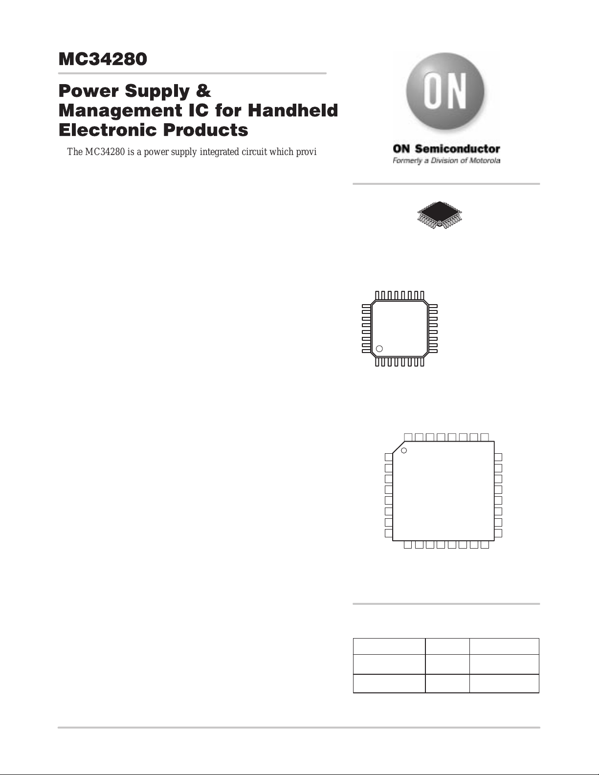
• 32–Pin LQFP Package
32
1
VMAINFB
VBAT
ENABLE
VDD
PDELAY
VREF
AGND
IREF
http://onsemi.com
32–LEAD LQFP
FTB SUFFIX
CASE 873A
MARKING DIAGRAM
MC34280F
TB
AWLYYWW
PIN CONNECTIONS
VMAIN
VMAINSW
VMAINGND
32
1
MC34280
PROB
DGND
LOWBATSEN
A = Assembly Location
WL = Wafer Lot
YY = Year
WW = Work Week
LIBAOUTNCLIBATIN
VAUXEMR
VAUXSW
NC
VAUXBASE
VAUXCHG
VAUXBDV
VAUXFBN
VAUXREF
VAUXFBP
VAUXEN
LIBATCL
LIBATON
LOWBATB
VAUXADJ
VAUXCON
APPLICATIONS:
• Digital Organizer and Dictionary
• Personal Digital Assistance (PDA)
• Dual Output Power Supply (For MPU, Logic, Memory, LCD)
• Handheld Battery Powered Device (1–2 AA/AAA cell)
Semiconductor Components Industries, LLC, 1999
February , 2000 – Rev. 2
1 Publication Order Number:
ORDERING INFORMATION
Device Package Shipping
MC34280FTB LQFP 250 Units/Tray
MC34280FTBR2 LQFP 1800 Tape & Reel
MC34280/D
Page 2
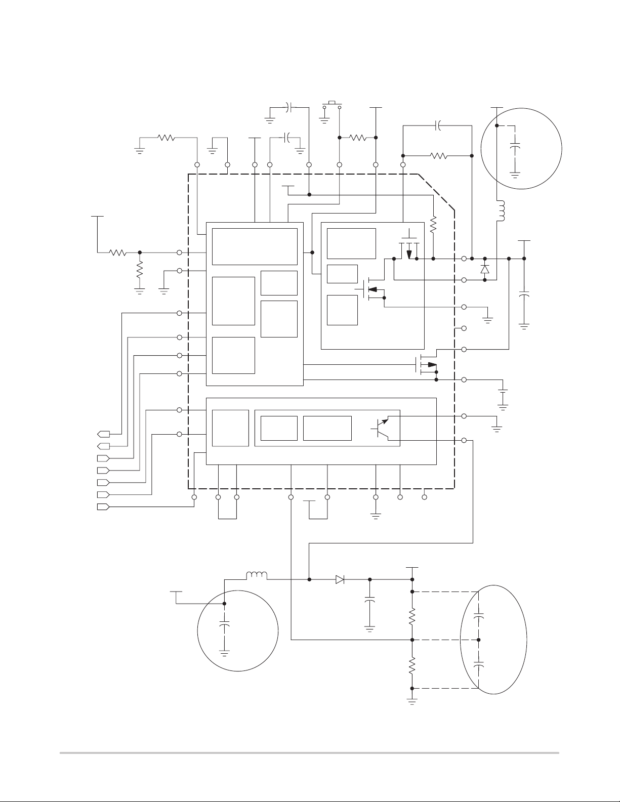
GND
Riref
r = 480 k
I
REF
MC34280
Figure 1. T ypical Application Block Diagram
Battery
4
Lock
Switch
GND
DD
VBAT
Ren
r = 1000 k
ENABLE
321
GND
AGND
V
REF
87
GND
V
REF
65
CVDD
c = 20u
Cpor
c = 80n
GND
PDELAY V
V
DD
VMAINFBVBAT
CMAINb
c = 100p
RMAINb
r = 1000 k
VBAT
Optional
CMAINbp
c = 100u
10 V SMT
tantalum
GND
PORB
LOWBAT
LIBATON
LIBATCL
VAUXADJ
VAUXCON
VAUXEN
VBAT
RLBa
r = 300 k
RLBb
r = 900 k
LOWBATSEN
DGND
GNDGND
PORB
LOWBATB
LIBATON
LIBATCL
VAUXADJ
VAUXCON
VAUXEN
9
10
11
12
13
14
15
16
17
VAUXFBP
R123
Power
ON
Reset
Current
Voltage
Reference
Lithium
Battery
Backup
Level
Control
Auxiliary Regulator
18 20 2119 22 23 24
VAUXREF
(1.1 V to 2.2 V)
Bias
Low
Battery
Detect
Current
Limit
VAUXFBN
VBAT
Control and
Gate Drive
Startup
Current
Limit
Main Regulator with
Synchronous Rectifier
Control and
Base Drive
VAUXBDV
s
M2
d
M1
s
Q1
VAUXBASE
VAUXCHG
r = 5
d
d
s
N/C
32
31
30
29
28
M3
27
26
25
VMAIN
1N5817
VMAINSW
VMAINGND
N/C
LIBATOUT
LIBATIN
VAUXEMR
VAUXSW
LMAIN
L = 33u
(Rs < 60 mOhm)
VMAIN
GND
GND
GND
CMAIN
c = 100u
10 V SMT
tantalum
GND
VBAT
Optional
LAUX
L = 22u
(Rs < 60 mOhm)
CAUXbp
c = 100u
10 V SMT
tantalum
GND
1N5818
30 V SMT
tantalum
http://onsemi.com
2
Caux
c = 30u
GND
VAUX
Rauxb
r = 2.2 M
Rauxa
r = 200 k
GND
Optional
CAUXb
c = 2n
CAUXa
c = 33n
Page 3
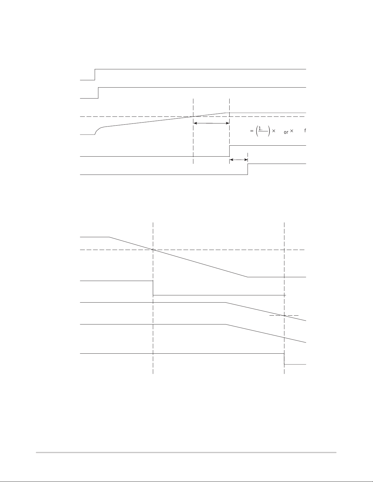
VBAT
ENABLE
VMAIN
PORB
VAUXEN
V
MAINreg
– 0.15 V
MC34280
TIMING DIAGRAMS
Figure 2. Startup Timing
T
POR
t
PORC
+
V
MAINreg
1.22
ǒ
0.5
Ǔ
C
RIref
por
VBAT
LOWBATB
VMAIN
ENABLE
PORB
LOWBAT Threshold
Figure 3. Power Down Timing
V
MAINreg
– 0.5 V
http://onsemi.com
3
Page 4
MC34280
TIMING DIAGRAMS (Con’t)
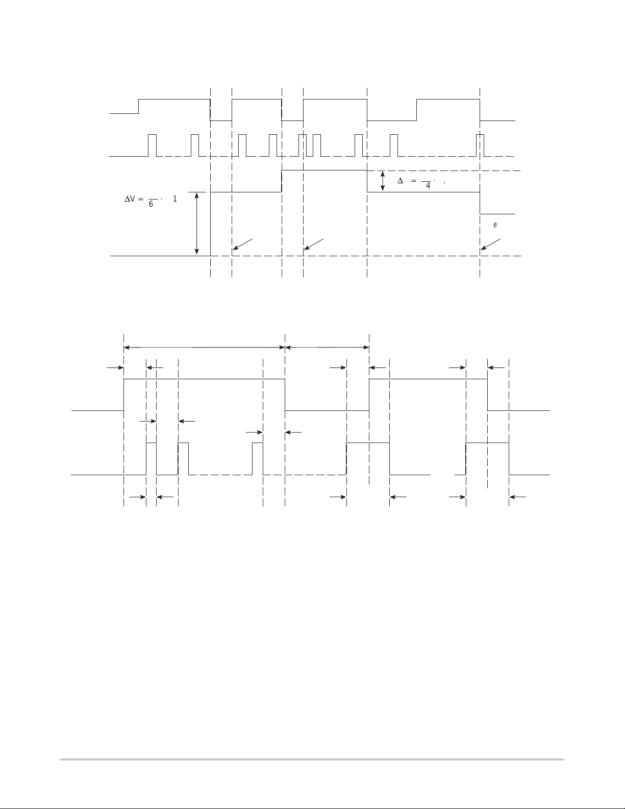
VAUXCON
VAUXADJ
VAUXREF
1.1 V
T otal N Pulses Total M Pulses
N
DV+
64
@
1.1 V
“Countup”
Flag is HIGH
Figure 4. Auxiliary Regulator Voltage Control
t
CW
t
CL
“Countup”
Flag is LOW
t
CC
M
@
64
1.1 V
t
RJL
Reset
VAUXREF
DV+
t
DL
2.2 V
1.65 V
VAUXCON
VAUXADJ
t
JC
t
JW
t
JL
t
DW
t
RW
Figure 5. Auxiliary Regulator Voltage Control Timing
http://onsemi.com
4
Page 5
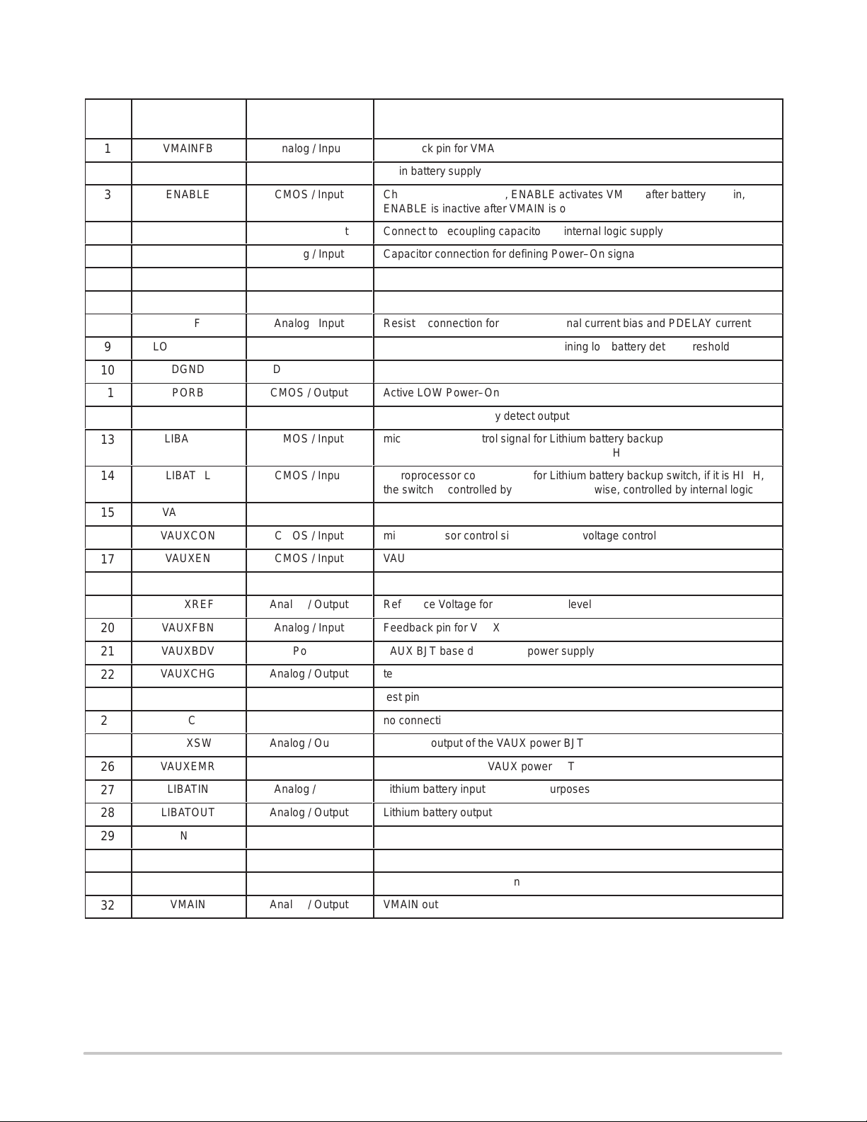
Pin
ББББББ
ББББББ
Á
ББББББ
Á
Á
Á
Á
Á
Á
Á
Á
Á
Á
Á
Á
Á
Á
Á
No.
1
2
3
ÁÁ
4
5
6
7
8
9
10
11
12
13
ÁÁ
14
ÁÁ
15
16
17
18
19
20
21
22
23
24
25
26
27
28
29
ÁÁ
30
31
32
MC34280
PIN FUNCTION DESCRIPTION
Function Type/Direction Description
VMAINFB
VBAT
ENABLE
ÁÁÁÁ
VDD
PDELAY
VREF
AGND
IREF
LOWBATSEN
DGND
PORB
LOWBATB
LIBATON
ÁÁÁÁ
LIBATCL
ÁÁÁÁ
VAUXADJ
VAUXCON
VAUXEN
VAUXFBP
VAUXREF
VAUXFBN
VAUXBDV
VAUXCHG
VAUXBASE
NC
VAUXSW
VAUXEMR
LIBATIN
LIBATOUT
NC
ÁÁÁÁ
VMAINGND
VMAINSW
VMAIN
Analog / Input
Power
CMOS / Input
БББББ
Analog / Output
Analog / Input
Analog / Output
Feedback pin for VMAIN
Main battery supply
Chip enable, Active high, ENABLE activates VMAIN after battery plug in,
ENABLE is inactive after VMAIN is on
БББББББББББББББББ
Connect to decoupling capacitor for internal logic supply
Capacitor connection for defining Power–On signal delay
Bandgap Reference output voltage. Nominal voltage is 1.25V
Analog Ground
Analog / Input
Analog / Input
Resistor connection for defining internal current bias and PDELAY current
Resistive network connection for defining low battery detect threshold
Digital Ground
CMOS / Output
CMOS / Output
CMOS / Input
БББББ
CMOS / Input
БББББ
CMOS / Input
CMOS / Input
CMOS / Input
Analog / Input
Analog / Output
Analog / Input
Power
Analog / Output
Analog / Output
Active LOW Power–On reset signal
Active LOW low battery detect output
microprocessor control signal for Lithium battery backup switch, the switch is
БББББББББББББББББ
ON when LIBATON=HIGH and LIBATCL=HIGH
microprocessor control signal for Lithium battery backup switch, if it is HIGH,
the switch is controlled by LIBATON, otherwise, controlled by internal logic
БББББББББББББББББ
microprocessor control signal for VAUX voltage control
microprocessor control signal for VAUX voltage control
VAUX enable, Active high
Feedback pin for VAUX
Reference Voltage for VAUX voltage level
Feedback pin for VAUX
VAUX BJT base drive circuit power supply
test pin
test pin
no connection
Analog / Output
Analog / Output
Analog / Input
Analog / Output
БББББÁБББББББББББББББББ
Power Ground
Analog / Input
Analog / Output
Collector output of the VAUX power BJT
Emitter output of the VAUX power BJT
Lithium battery input for backup purposes
Lithium battery output
no connection
Ground for VMAIN low side switch
VMAIN inductor connection
VMAIN output
http://onsemi.com
5
Page 6
MC34280
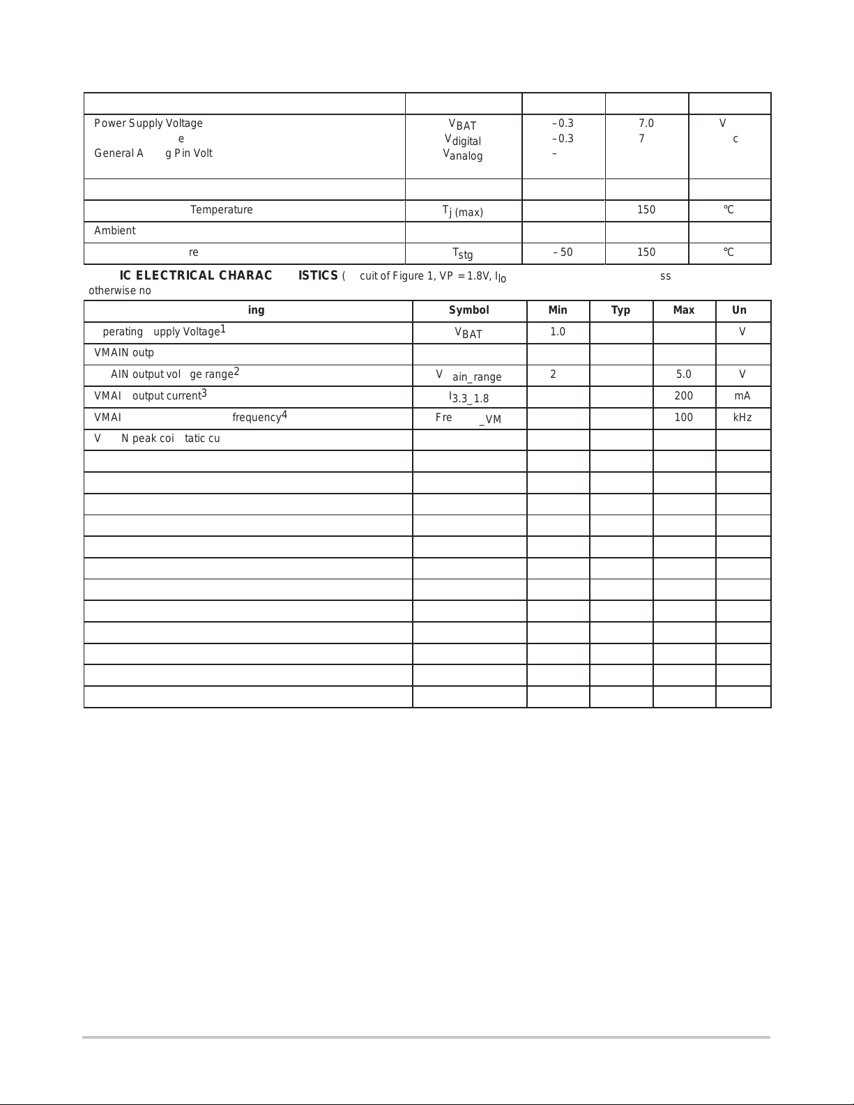
ABSOLUTE MAXIMUM RATINGS (T
Parameter
Power Supply Voltage
Digital Pin Voltage V
General Analog Pin Voltage V
Pin VAUXSW to Pin VAUXEMR Voltage (Continuous) V
Pin VMAINSW to Pin VMAIN Voltage (Continuous)
Operating Junction Temperature
Ambient Operating Temperature
Storage Temperature
STATIC ELECTRICAL CHARACTERISTICS (Circuit of Figure 1, VP = 1.8V, I
= 25°C, unless otherwise noted.)
A
Symbol Min Max Unit
V
BAT
digital
analog
AUXCE
V
syn
Tj
(max)
T
a
T
stg
load
–0.3
7.0
–0.3 7.0 Vdc
–0.3 7.0 Vdc
–0.3 30 Vdc
0.3
150
0
–50
70
150
= 0 mA, TA = 0 to 70°C unless
Vdc
Vdc
°C
°C
°C
otherwise noted.)
Rating
Operating Supply Voltage
1
VMAIN output voltage V
VMAIN output voltage range
VMAIN output current
VMAIN maximum switching frequency
2
3
4
VMAIN peak coil static current limit I
Symbol Min Typ Max Unit
V
BAT
main
V
main_range
I
3.3_1.8
Freq
max_VM
LIM_VM
1.0 V
3.13 3.3 3.47 V
2.7 5.0 V
200 mA
100 kHz
0.85 1.0 1.15 A
VAUX output voltage range VAUX_range 5.0 25 V
VAUXREF lower level voltage VAUX
VAUXREF upper level voltage VAUX
VAUXREF step size VAUX
VAUX maximum switching frequency Freq
VAUX peak coil static current limit I
Quiescent Supply Current at Standby Mode
5
Reference Voltage @ no load Vref
Battery Low Detect lower hysteresis threshold
6
Battery Low Detect upper hysteresis threshold V
PDELAY Pin output charging current Ichg
PDELAY Pin voltage threshold Vth
NOTE: 1. Output current capability is reduced with supply voltage due to decreased energy transfer. The supply voltage must not be higher than
NOTE: 2. Output voltage can be adjusted by external resistor to the VMAINFB pin.
NOTE: 3. At VBAT = 1.8V, output current capability increases with VBAT .
NOTE: 4. Only when current limit is not reached.
NOTE: 5. This is average current consumed by the IC from VDD, which is low–pass filtered from VMAIN, when only VMAIN is enabled and at no loading.
NOTE: 6. This is the minimum of ”LOWBATB” threshold for battery voltage, the threshold can be increased by external resistor divider from ”VBA T” to
VMAIN+0.6V to ensure boost operation. Max Start–up loading is typically 1V at 400 µA, 1.8V at 4.4 mA, and 2.2V at 88 mA.
”LOWBATSEN”.
REF_L
REF_H
REF_S
max_VL
LIM_VL
Iq
standby
no_load
V
LOBAT_L
LOBAT_H
PDELAY
PDELAY
1.0 1.1 1.2 V
2.0 2.2 2.4 V
17 mV
120 kHz
1.0 A
35 60 µA
1.19 1.22 1.25 V
0.8 0.85 0.9 V
1.05 1.1 1.15 V
0.8 1.0 1.2 µA
1.19 1.22 1.25 V
http://onsemi.com
6
Page 7

MC34280
IN
Eff
,
EFFICIENCY
OF
VAUX
%
OUT_AUX
Eff
,
EFFICIENCY
OF
VMAIN
%
DYNAMIC ELECTRICAL CHARACTERISTICS (Refer to TIMING DIAGRAMS, T
Rating
Minimum PORB to Control delay t
Minimum VAUXCON pulse HIGH width t
Minimum V AUXCON pulse LOW width t
Minimum VAUXADJ to VAUXCON delay t
Minimum VAUXADJ pulse HIGH width t
Minimum V AUXADJ pulse LOW width t
Minimum VAUXCON LOW to VAUXADJ pulse delay
Minimum hold time of VAUXADJ for Reset VAUXREF t
Minimum VAUXADJ pulse HIGH width for Reset VAUXREF t
Minimum hold time of VAUXADJ for Decrement VAUXREF t
Minimum V AUXADJ pulse HIGH width for Decrement VAUXREF t
NOTE: 1. For not resetting VAUXREF.
1
Symbol Min Typ Max Unit
PORC
CW
CC
CL
JW
JC
t
JL
RJL
RW
DL
DW
TYPICAL ELECTRICAL CHARACTERISTICS
Figure 6. Efficiency of VMAIN versus Output
Current (VMAIN = 3.3 V, L = 33 uH, Various VIN)
90%
)
(
85%
80%
75%
VMAIN
70%
0
50 100 150 200 250 300
I
OUT_MAIN
, MAIN OUTPUT CURRENT (mA)
Vin = 3V
Vin = 1.8V
Vin = 1.5V
Vin = 1V
, EFFICIENCY OF VMAIN (%)
Eff
Figure 7. Efficiency of VMAIN versus Input
V oltage (VMAIN = 3.3 V, L1 = 33 uH, Various I
90%
85%
80%
75%
VMAIN
70%
1
= 0 to 70°C unless otherwise noted.)
A
500 nS
5.0 µS
8.0 µS
1.0 µS
1.0 µS
1.0 µS
1.0 µS
500 nS
1.0 µS
500 nS
1.0 µS
X
X
X
1.5 2 3
VIN, INPUT VOLTAGE (V)
2.5
I
out
I
out
I
out
I
out
I
out
OUT
= 10mA
= 60mA
= 100mA
= 150mA
= 200mA
)
X
Figure 8. Efficiency of VAUX versus Output
Current (VAUX = 25 V, L2 = 33 uH, Various VIN)
80%
)
(
75%
70%
65%
60%
55%
VAUX
50%
1
357 111315
I
, AUX OUTPUT CURRENT (mA)
9
Vin = 3V
Vin = 1.8V
Vin = 1.5V
Vin = 1V
http://onsemi.com
Figure 9. Efficiency of V AUX versus Input
Voltage (VAUX = 25 V, L2 = 33 uH, Various I
80%
75%
70%
65%
60%
, EFFICIENCY OF VAUX (%)
55%
VAUX
Eff
50%
1
7
1.5 2 2.5 3
, INPUT VOLTAGE (V)
V
I
out
I
out
I
out
I
out
= 1mA
= 5mA
= 10mA
= 15mA
OUT
)
Page 8

MC34280
Eff
,
EFFICIENCY
OF
VAUX
%
IN
OUT_AUX
TYPICAL ELECTRICAL CHARACTERISTICS (Cont’d)
Figure 10. Efficiency of VAUX versus Output
Current (VAUX = 20 V, L2 = 33 uH, Various VIN)
80%
)
(
75%
70%
65%
VAUX
60%
55%
50%
1
Vin = 3V
Vin = 1.8V
Vin = 1.5V
Vin = 1V
3 5 7 11 13 15
I
OUT_AUX
, AUX OUTPUT CURRENT (mA)
9
Figure 12. Efficiency of VAUX versus Output
Current (VAUX = 5 V, L2 = 82 uH, Various VIN)
85%
80%
75%
70%
65%
, EFFICIENCY OF VAUX (%)
Eff
60%
55%
50%
VAUX
45%
40%
5 1015 3035
1
I
, AUX OUTPUT CURRENT (mA)
Vin = 3V
Vin = 2.4V
Vin = 1.8V
Vin = 1.5V
Vin = 1V
Figure 11. Efficiency of VAUX versus Input
Voltage (VAUX = 20 V, L2 = 33 uH, Various I
80%
75%
70%
65%
60%
, EFFICIENCY OF VAUX (%)
55%
VAUX
Eff
50%
1
1.5 2 2.5 3
VIN, INPUT VOLTAGE (V)
Figure 13. Efficiency of V AUX versus Input
Voltage (VAUX = 5 V, L2 = 82 uH, Various I
85%
80%
75%
70%
, EFFICIENCY OF VAUX (%)
65%
VAUX
Eff
50%
1
1.5
V
2 2.5 320 25
, INPUT VOLTAGE (V)
I
out
I
out
I
out
I
out
= 1mA
= 5mA
= 10mA
= 15mA
I
= 1V
out
I
= 5V
out
I
= 10V
out
I
= 15V
out
I
= 25V
out
OUT
OUT
)
)
http://onsemi.com
8
Page 9

MC34280
Figure 14. VMAIN Output Ripple (Medium Load) Figure 15. VMAIN Output Ripple (Heavy Load)
20 uS / div
1: VMAIN = 3.3 V (50 mV/div, AC COUPLED)
2: Voltage at VMAINSW (1 V/div)
1: VMAIN = 3.3 V (50 mV/div, AC COUPLED)
2: Voltage at VMAINSW (1 V/div)
10 uS / div
Figure 16. VAUX Output Ripple (Medium Load) Figure 17. VAUX Output Ripple (Heavy Load)
20 uS / div
1: VAUX = 20 V (50 mV/div, AC COUPLED)
2: Voltage at VAUXSW (10 V/div)
Figure 18. VMAIN Startup and Power–On Reset
1: VAUX = 20 V (50 mV/div, AC COUPLED)
2: Voltage at VAUXSW (10 V/div)
Figure 19. V AUX Startup
10 uS / div
50 mS / div
1: VMAIN from 1 V to 3.3 V (1 V/div)
2: Voltage of PORB (2 V/div)
3: Voltage of ENABLE (2 V/div)
5 mS / div
1: VAUX from 1.8 V to 20 V (5 V/div)
2: VAUXEN (2 V/div)
http://onsemi.com
9
Page 10

MC34280
DET AILED OPERATING DESCRIPTION
General
The MC34280 is a power supply integrated circuit which
provides two boost regulated outputs and some power
management supervisory functions. Both regulators apply
Pulse–Frequency–Modulation (PFM). The main boost
regulator output can be externally adjusted from 2.7V to 5V .
An internal synchronous rectifier is used to ensure high
efficiency (achieve 87%). The auxiliary regulator with a
built–in power transistor can be configured to produce a
wide range of positive voltage (can be used to supply a LCD
contrast voltage). This voltage can be adjusted from +5V to
+25V by an external potentiometer; or by a microprocessor,
digitally through a 6–bit internal DAC.
The MC34280 has been designed for battery powered
hand–held products. With the low start–up voltage from 1V
and the low quiescent current (typical 35 µA); the MC34280
is best suited to operate from 1 to 2 AA/ AAA cell.
Moreover, supervisory functions such as low battery
detection, CPU power–on reset, and back–up battery
control, are also included in the chip. It makes the MC34280
the best one–chip power management solution for
applications such as electronic organizers and PDAs.
Pulse Frequency Modulation (PFM)
Both regulators apply PFM. With this switching scheme,
every cycle is started as the feedback voltage is lower than
the internal reference. This is normally performed by
internal comparator. As cycle starts, Low–Side switch (i.e.
M1 in Figure 1) is turned ON for a fixed ON time duration
(namely, Ton) unless current limit comparator senses coil
current reaches its preset limit. In the latter case, M1 is OFF
instantly . So Ton is defined as the maximum ON time of M1.
When M1 is ON, coil current ramps up so energy is being
stored inside the coil. At the moment just after M1 is OFF,
the Synchronous Rectifier (i.e. M2 in Figure 1) or any
rectification device (such as Schottky Diode of Auxiliary
Regulator) is turned ON to direct coil current to charge up
the output bulk capacitor. Provided that coil current is not
reached, every switching cycle delivers fixed amount of
energy to the bulk capacitor. So for higher loading, larger
amount of energy (Charge) is withdrawn from the bulk
capacitor, and as output voltage is needed to regulated, larger
amount of Charge is needed to be supplied to the bulk
capacitor, that means switching frequency is needed to be
increased; and vice–versa.
Main Regulator
Figure 20 shows the simplified block diagram of Main
Regulator. Notice that precise bias current Iref is generated
by a VI converter and external resistor RIref, where
+
0.5
RIref
(A)
Iref
This bias current is used for all internal current bias as well
as setting VMAIN value. For the latter application, Iref is
doubled and fed as current sink at Pin 1. With external
resistor RMAINb tied from Pin1 to Pin32, a constant level
shift is generated in between the two pins. In close–loop
operation, voltage at Pin 1 (i.e. Output feedback voltage) is
needed to be regulated at the internal reference voltage level,
1.22V. Therefore, the delta voltage across Pin 1 and Pin 32
which can be adjusted by RMAINb determines the Main
Output voltage. If the feedback voltage drops below 1.22V,
internal comparator sets switching cycle to start. So, VMAIN
can be calculated as follows.
VMAIN
+
1.22
RMAINb
)
RIref
(V)
From the above equation, although VMAIN can be
adjusted by RMAINb and RIref ratio, for setting VMAIN, it
is suggested, by changing RMAINb value with RIref kept at
480K. Since changing RIref will alter internal bias current
which will affect timing functions of Max ON time (T
and Min OFF time (T
). Their relationships are as
OFF1
ON1
follows;
+
1
1
1.7 10
+
6.4 10
T
ON
T
OFF
Continuous Conduction Mode and Discontinuous
Conduction Mode
–11
–12
RIref
RIref
(S)
(S)
In Figure 21, regulator is operating at Continuous
Conduction Mode. A switching cycle is started as the output
feedback voltage drops below internal voltage reference
VREF . At that instant, the coil current does not drop to zero
yet, and it starts to ramp up for the next cycle. As the coil
current ramps up, loading makes the output voltage to
decrease as the energy supply path to the output bulk
capacitor is disconnected. And after Ton elapsed, M1 is OFF ,
M2 becomes ON, energy is dumped to the bulk capacitor.
Output voltage is increased as excessive charge is pumped
in, then it is decreased after the coil current drops below the
loading. Notice the abrupt spike of output voltage is due to
ESR of the bulk capacitor. Feedback voltage can be
resistor–divided down or level–shift down from the output
voltage. As this feedback voltage drops below VREF, next
switching cycle starts.
)
http://onsemi.com
10
Page 11

VBAT
D
Iref
IREF
RIref
480 kOhm
8
x2
Voltage
Reference
0.5 V
1.22 V
MC34280
DETAILED OPERATING DESCRIPTION (Cont’d)
CMAINb
100 pF
2 x Iref
VMAINFB
+ve Edge Delay
for Max. ON Time
VCOMP
COMP1
1–SHOT
for Min. OFF Time
RSQ
Qb
RMAINb
1000 kOhm
ZLC
V
DD
DGND
RSQ
COMP3
311
L1
33uH
VMAINSW
M1
senseFET
V
DD
M2
VMAIN
32
CMAIN
100 uF
VMAINGN
30
+
AGND
Voltage Reference
& Current Bias
Main Regulator
with Synchronous Rectifier
Figure 20. Simplified Block Diagram of Main Regulator
In Figure 22, regulator is operating at Discontinuous
Conduction Mode, waveforms are similar to those of Figure
21. However, coil current drops to zero before next
switching cycle starts.
To estimate conduction mode, below equation can be
used.
Iroom
where,
if I
room
T
h
+
η
ON
L Vout
2
is efficiency, refer to Figure 6
> 0, the regulator is at Discontinuous Conduction
Vin
2
*
I
LOAD
mode
if I
= 0, the regulator is at Critical Conduction mode
room
where coil current just drops to zero and next cycle starts.
if I
< 0, the regulator is at Continuous Conduction
room
mode
2
COMP2
AGND
DGND
ON
L
(A)
T
SW
I
pk
+
+
1*h
1
*
T
ON
I
LOAD
T
ǒ
T
ǒ
ON
SW
Vin
Vout
Ǔ
ILIM
(S);
Ǔ
Vin T
)
For Discontinuous Conduction mode, provided that
current limit is not reached,
2
T
Vin
@
(A)
@
ON
ǒ
Vout
h
@
Vin
*
(S);
Ǔ
1
T
SW
+
2
@L@
I
LOAD
Vin
I
+
@
pk
T
ON
L
For Continuous Conduction mode, provided that current
limit is not reached,
http://onsemi.com
11
Page 12

VREF
Feedback Voltage
MC34280
Cycle Starts
t
dl
Loading Current, I
Coil Current
VMAIN Zoom–In
LOAD
VMAIN
V@SW
Feedback Voltage
VREF
M1 ON
M2 OFF
I
pk
VMAIN + 1 V
M1 OFF
t
dh
M2 ON
0 V
M1 ON
M2 OFF
T
ON
T
SW
Figure 21. Waveforms of Continuous Conduction Mode
Cycle Starts
t
dl
M1 OFF
M2 ON
M1 ON
M2 OFF
M1 OFF
M2 ON
Loading Current, I
Coil Current
VMAIN Zoom–In
LOAD
VMAIN
V@SW
M1 ON
M2 OFF
I
pk
VMAIN + 1 V
M1 OFF M1 OFF M1 OFF
t
dh
0 V
M1 ON
M2 OFF
T
ON
V
IN
M2 OFF
T
SW
Figure 22. Waveforms of Discontinuous Conduction Mode
http://onsemi.com
12
M1 ON
Page 13

MC34280
X
F
VBAT
DETAILED OPERATING DESCRIPTION (Cont’d)
Synchronous Rectification
A Synchronous Rectifier is used in the main regulator to
enhance efficiency. Synchronous rectifier is normally
realized by powerFET with gate control circuitry which,
however, involved relative complicated timing concerns. In
Figure 20, as main switch M1 is being turned OFF, if the
synchronous switch M2 is just turned ON with M1 not being
completed turned OFF , current will be shunt from the output
bulk capacitor through M2 and M1 to ground. This power
loss lowers overall efficiency. So a certain amount of dead
time is introduced to make sure M1 is completely OFF
before M2 is being turned ON, this timing is indicated as t
dh
in Figure 21.
When the main regulator is operating in continuous mode,
as M2 is being turned OFF, and M1 is just turned ON with
M2 not being completed OFF , the above mentioned situation
will occur. So dead time is introduced to make sure M2 is
completed OFF before M1 is being turned ON, this is
indicated as tdl in Figure 21.
When the main regulator is operating in discontinuous
mode, as coil current is dropped to zero, M2 is supposed to
be OFF. Fail to do so, reverse current will flow from the
output bulk capacitor through M2 and then the inductor to
the battery input. It causes damage to the battery. So
M2–voltage–drop sensing comparator (COMP3 of Figure
20) comes with fixed offset voltage to switch M2 OFF
before any reverse current builds up. However, if M2 is
switch OFF too early, large residue coil current flows
through the body diode of M2 and increases conduction loss.
Therefore, determination on the offset voltage is essential
for optimum performance.
Auxiliary Regulator
The Auxiliary Regulator is a boost regulator, applies PFM
scheme to enhance high efficiency and reduce quiescent
current. An internal voltage comparator (COMP1 of Figure
23) detects when the voltage of Pin V AUXFBN drops below
that of Pin VAUXFBP. The internal power BJT is then
switched ON for a fixed–ON–time (or until the internal
current limit is reached), and coil current is allowed to build
up. As the BJT is switched OFF, coil current will flow
through the external Schottky diode to charge up the bulk
capacitor. After a fixed–mimimum–OFF time elapses, next
switching cycle will start if the output of the voltage
comparator is HIGH. Refer to Figure 23, the VAUX
regulation level is determined by the equation as follows,
R
AUXb
AUXa
Ǔ
(V)
V
AUX
+
VAUXFBP
@ǒ1
)
R
Where Max ON Time, TON2, and Min OFF T ime, TOFF2
can be determined by the following equations.
T
ON
T
OFF
2
2
+
1.7 10
+
2.1 10
–11
–12
RIref
RIref
(S)
(S)
VAUXADJ
VAUXCON
VAUXEN
VAUXREF
19
2.2 V
6–Bit
Counter
15
Input
Logic
16
17
Auxiliary Level Control Auxiliary Regulator
6–Bit
6
1.1 V
Figure 23. Simplified Block Diagram of Auxiliary Regulator
2018
COMP1
RAUXa
200 kOhm
VAUXFBN VAUXSWVAUXBDVVAUXFBP
VCOMP
RAUXb
2200 kOhm
+ve Edge Delay
for Max. ON Time
RSQ
1–SHOT
for Min. OFF Time
Qb
VBAT
ILIM
2521
Q1
COMP2
AGND
L2
33uH
senseBJT
+
CAU
33 u
VAUXEMR
26
http://onsemi.com
13
Page 14

MC34280
DETAILED OPERATING DESCRIPTION (Cont’d)
Auxiliary Regulator (Cont’d)
As the Auxiliary Regulator control scheme is the same as
the Main Regulator, equations for conduction mode, Tsw
and Ipk can also be applied, However, h to be used for
caculation is refered to Figure 8, 10, or 12.
If external potentiometer is used for voltage level
adjustment, internal 1.22V reference voltage can be used as
shown in the application diagram of Figure 24.
Cpor
c = 80n
GND
GND
RLBa
r = 300 k
GND
GND
GND
Riref
r = 480 k
10
11
12
13
14
15
16
87654321
9
MC34280
17 18 19 20 21 22 23 24
VBAT
GND
GND
Vref
RLBb
r = 900 k
PORB
LOWBAT
LIBATON
LIBATCL
VAUXEN
Current Limit for Both regulators
From Figure 20 and Figure 23, sense devices (senseFET
or senseBJT) are applied to sample coil current as the
low–side switch is ON. With that sample current flowing
through a sense resistor, sense–voltage is developed.
Threshold detector (COMP2 in both figures) detects
whether the sense–voltage is higher than preset level. If it
happens, detector output reset the flip–flop to switch OFF
low–side switch, and the switch can only be ON as next
cycle starts.
CVDD
c = 20u
GND
VBAT
Ren
r = 1000 k
32
31
30
29
28
27
26
25
GND
GND
GND
VBAT
CMAINb
c = 100p
RMAINb
r = 1000 k
1N5817
L = 33uH
LAUX
L = 33uH
LMAIN
GND
VBAT
1N5818
Caux
c = 30u
CMAIN
c = 100u
GND
VAUX
GND
Rauxb
r = 2.2 M
Figure 24. Application Diagram with External Potentiometer for V AUX Adjustment
http://onsemi.com
14
Rauxa
r = 200 k
GND
Page 15

MC34280
ББББББ
ББББББ
ББББББ
ББББББ
ББББББ
ББББББ
Á
Á
ББББББ
Á
Á
Á
DETAILED OPERATING DESCRIPTION (Cont’d)
Auxiliary voltage adjustment
The V AUX voltage can be adjusted by the microprocessor
control signals, namely, VAUXCON and VAUXADJ. The
control signal pattern is shown in Figure 4. The input truth
table is shown in Figure 25.
When VAUXEN is LOW, the Auxiliary Regulator is shut
down, only the counter content is retained. The initial
counter content is mid–range of 6–bit.
At the rising edge of VAUXCON, if V AUXADJ is LOW
(/ HIGH), each following V AUXADJ pulse enclosed by the
VAUXCON pulse packet increments (/ decrements) the
6–bit counter. At the falling edge of VAUXCON, the counter
content is then latched to a 6–bit DAC and is converted to a
voltage level of VAUXREF between 1.1V and 2.2V.
At the falling edge of V AUXCON, if V AUXADJ is HIGH,
the counter content will be reset to mid–range (1.65V). This
is also the default setting just after power–ON reset is
removed.
The 6–bit DAC converts the counter content to voltage
level ranging from 1.1 to 2.2V, so there are altogether 64
levels, and each voltage step is 17mV. When the counter
content reaches its maximum or minimum, further pulse of
VAUXADJ will be disregarded, until counting direction is
changed.
auxiliary regulator. Meanwhile, the startup circuitry will be
shut down. The Power–ON Reset block also starts to charge
up the external capacitor tied from Pin PDELAY to ground
with precise constant current. As the Pin PDELA Y’s voltage
reaches an internal set threshold, Pin PORB will go HIGH
to awake the microprocessor. And,
1.22
ǒ
T
POR
+
0.5
Ǔ
C
RIref
por
(S)
From Figure 3, if, by any chance, VMAIN is dropped
below the user–defined VMAIN output level minus 0.5V,
PORB will go LOW to indicate the OUTPUT LOW
situation. And, the IC will continue to function until the
VMAIN is dropped below 2V.
Low–Battery–Detect
The Low–Battery–Detect block is actually a voltage
comparator. Pin LOWBAT is LOW , if the voltage of external
Pin LOWBATSEN is lower than 0.85V internal reference.
The IC will neglect this warning signal. Pin LOWBAT will
become HIGH, if the voltage of external Pin LOWBA TSEN
is recovered to more than 1.1V . From Figure 1, with external
resistors RLBa and RLBb, thresholds of
Low–Battery–Detect can be adjusted based on the equations
below .
Power–ON Reset
The Power–ON Reset block accepts external active HIGH
ENABLE signal to activate the IC after battery is plugged in.
During the startup period (see Figure 2), the internal startup
circuitry is enabled to pump up VMAIN to a certain voltage
level, which is the user–defined VMAIN output level minus
an offset of 0.15V . The internal power–on reset signal is then
disabled to activate the main regulator and conditionally the
VAUXEN
0
1
1
1
1
1
1
ÁÁÁÁ
VAUXCON VAUXADJ RESULT
X
0
1
БББББ
X
X
0
1
0
1
ÁÁÁÁ
Figure 25. Auxiliary Voltage Control Input Truth Table
R
LBa
V
LOBAThigh
V
LOBATlow
Hold the counter content
Hold the counter content
Set ”countup” flag HIGH
Set ”countup” flag LOW
Increment (/ Decrement) the counter if ”countup” flag is HIGH (/ LOW)
DAC the counter content to VAUXREF voltage level (1.1 – 2.2 V)
Reset the counter to mid–range, then convert the counter content to
VAUXREF voltage level (1.65V)
ББББББББББББББББ
+
+
1.1
0.85
ǒ1
ǒ1
)
)
R
R
R
LBb
LBa
LBb
Ǔ
(V)
Ǔ
(V)
http://onsemi.com
15
Page 16

MC34280
Á
Á
Á
DETAILED OPERATING DESCRIPTION (Cont’d)
Lithium–Battery backup
The backup conduction path which is provided by an
internal power switch (typ. 13 Ohm) can be controlled by
internal logic or microprocessor.
If LIBA TCL is LOW, the switch, which is then controlled
by internal logic, is ON when the battery is removed and
VMAIN is dropped below LIBATIN by more than 100mV ,
feedback response, destabilizing the regulator and creating
a larger ripple at the output. From Figure 1, ripple of Main
and AUX regulator can be reduced by CMAINb, CAUXa
and CAUXb ranging from 100pF to 100nF respectively.
Reducing the ripple is also with improving efficiency,
system designers are recommended to do experiments on
capacitance values based on the PCB design.
and returns OFF when the battery is plugged back in.
If LIBATCL is HIGH, the switch is controlled by
microprocessor through LIBA TON. The truth table is shown
in Figure 26.
Efficiency and Output Ripple
For both regulators, when large values are used for
feedback resistors (> 50kOhm), stray capacitance of pin 1
(VMAINFB) and pin 20 (VAUXFBN) can add ”lag” to the
LIBATCL LIBATON Action
0
БББББ
1
1
БББББ
X
0
1
The switch is ON when the battery is removed and VMAIN is dropped below LIBATIN
by more than 100mV; The switch is OFF when the battery is plugged in.
ББББББББББББББББББББ
The switch is OFF
The switch is ON
Figure 26. Lithium Battery Backup Control Truth Table
Bypass Capacitors
If the metal leads from battery to coils are long, its stray
resistance can put additional power loss to the system as AC
current is being conducted. In that case, bypass capacitors
(CMAINbp and CAUXbp of Figure 1) are recommended to
remove AC components of coil currents to minimize that
power loss to optimize efficiency.
http://onsemi.com
16
Page 17

SEATING
PLANE
9
C
–T–
B1
–AB–
–AC–
E
MC34280
P ACKAGE DIMENSIONS
32–LEAD LQFP
FTB SUFFIX
CASE 873A–02
A
A1
32
1
4X
25
T–U0.20 (0.008) ZAB
BASE
METAL
N
–U–
VB
DETAIL Y
8
9
–Z–
S1
V1
17
4X
T–U0.20 (0.008) Z
AC
SECTION AE–AE
DF
J
S
G
DETAIL AD
0.10 (0.004) AC
AE
_
8X
M
R
P
AE
DETAIL Y
H
W
_
Q
K
X
NOTES:
1. DIMENSIONING AND TOLERANCING PER ANSI
Y14.5M, 1982.
2. CONTROLLING DIMENSION: MILLIMETER.
3. DATUM PLANE –AB– IS LOCATED AT BOTTOM
T–U
M
0.20 (0.008) ZAC
OF LEAD AND IS COINCIDENT WITH THE LEAD
WHERE THE LEAD EXITS THE PLASTIC BODY AT
THE BOTTOM OF THE PARTING LINE.
4. DATUMS –T–, –U–, AND –Z– TO BE
DETERMINED AT DATUM PLANE –AB–.
5. DIMENSIONS S AND V TO BE DETERMINED AT
SEATING PLANE –AC–.
6. DIMENSIONS A AND B DO NOT INCLUDE
MOLD PROTRUSION. ALLOWABLE PROTRUSION
IS 0.250 (0.010) PER SIDE. DIMENSIONS A AND B
DO INCLUDE MOLD MISMATCH AND ARE
DETERMINED AT DATUM PLANE –AB–.
7. DIMENSION D DOES NOT INCLUDE DAMBAR
PROTRUSION. DAMBAR PROTRUSION SHALL
NOT CAUSE THE D DIMENSION TO EXCEED
0.520 (0.020).
8. MINIMUM SOLDER PLATE THICKNESS SHALL
BE 0.0076 (0.0003).
9. EXACT SHAPE OF EACH CORNER MAY VARY
FROM DEPICTION.
–T–, –U–, –Z–
MILLIMETERS
DIMAMIN MAX MIN MAX
7.000 BSC 0.276 BSC
A1 3.500 BSC 0.138 BSC
B 7.000 BSC 0.276 BSC
B1 3.500 BSC 0.138 BSC
C 1.400 1.600 0.055 0.063
D 0.300 0.450 0.012 0.018
E 1.350 1.450 0.053 0.057
F 0.300 0.400 0.012 0.016
G 0.800 BSC 0.031 BSC
H 0.050 0.150 0.002 0.006
J 0.090 0.200 0.004 0.008
K 0.500 0.700 0.020 0.028
__
M 12 REF 12 REF
N 0.090 0.160 0.004 0.006
P 0.400 BSC 0.016 BSC
Q 1 5 1 5
____
R 0.150 0.250 0.006 0.010
S 9.000 BSC 0.354 BSC
S1 4.500 BSC 0.177 BSC
V 9.000 BSC 0.354 BSC
V1 4.500 BSC 0.177 BSC
W 0.200 REF 0.008 REF
X 1.000 REF 0.039 REF
INCHES
DETAIL AD
0.250 (0.010)
GAUGE PLANE
http://onsemi.com
17
Page 18

Notes
MC34280
http://onsemi.com
18
Page 19

Notes
MC34280
http://onsemi.com
19
Page 20

MC34280
ON Semiconductor and are trademarks of Semiconductor Components Industries, LLC (SCILLC). SCILLC reserves the right to make changes
without further notice to any products herein. SCILLC makes no warranty , representation or guarantee regarding the suitability of its products for any particular
purpose, nor does SCILLC assume any liability arising out of the application or use of any product or circuit, and specifically disclaims any and all liability ,
including without limitation special, consequential or incidental damages. “Typical” parameters which may be provided in SCILLC data sheets and/or
specifications can and do vary in different applications and actual performance may vary over time. All operating parameters, including “Typicals” must be
validated for each customer application by customer’s technical experts. SCILLC does not convey any license under its patent rights nor the rights of others.
SCILLC products are not designed, intended, or authorized for use as components in systems intended for surgical implant into the body, or other applications
intended to support or sustain life, or for any other application in which the failure of the SCILLC product could create a situation where personal injury or
death may occur. Should Buyer purchase or use SCILLC products for any such unintended or unauthorized application, Buyer shall indemnify and hold
SCILLC and its officers, employees, subsidiaries, affiliates, and distributors harmless against all claims, costs, damages, and expenses, and reasonable
attorney fees arising out of, directly or indirectly , any claim of personal injury or death associated with such unintended or unauthorized use, even if such claim
alleges that SCILLC was negligent regarding the design or manufacture of the part. SCILLC is an Equal Opportunity/Affirmative Action Employer .
PUBLICATION ORDERING INFORMATION
NORTH AMERICA Literature Fulfillment:
Literature Distribution Center for ON Semiconductor
P.O. Box 5163, Denver, Colorado 80217 USA
Phone: 303–675–2175 or 800–344–3860 Toll Free USA/Canada
Fax: 303–675–2176 or 800–344–3867 Toll Free USA/Canada
Email: ONlit@hibbertco.com
Fax Response Line: 303–675–2167 or 800–344–3810 T oll Free USA/Canada
N. American Technical Support: 800–282–9855 Toll Free USA/Canada
EUROPE: LDC for ON Semiconductor – European Support
German Phone: (+1) 303–308–7140 (M–F 1:00pm to 5:00pm Munich Time)
Email: ONlit–german@hibbertco.com
French Phone: (+1) 303–308–7141 (M–F 1:00pm to 5:00pm Toulouse T ime)
Email: ONlit–french@hibbertco.com
English Phone: (+1) 303–308–7142 (M–F 12:00pm to 5:00pm UK Time)
Email: ONlit@hibbertco.com
EUROPEAN TOLL–FREE ACCESS*: 00–800–4422–3781
*Available from Germany, France, Italy, England, Ireland
CENTRAL/SOUTH AMERICA:
Spanish Phone: 303–308–7143 (Mon–Fri 8:00am to 5:00pm MST)
Email: ONlit–spanish@hibbertco.com
ASIA/PACIFIC : LDC for ON Semiconductor – Asia Support
Phone: 303–675–2121 (Tue–Fri 9:00am to 1:00pm, Hong Kong Time)
T oll Free from Hong Kong & Singapore:
001–800–4422–3781
Email: ONlit–asia@hibbertco.com
JAPAN: ON Semiconductor, Japan Customer Focus Center
4–32–1 Nishi–Gotanda, Shinagawa–ku, T okyo, Japan 141–8549
Phone: 81–3–5740–2745
Email: r14525@onsemi.com
ON Semiconductor Website: http://onsemi.com
For additional information, please contact your local
Sales Representative.
http://onsemi.com
20
MC34280/D
 Loading...