

Page 1
EN
2
Device
Operating
Temperature Range
Package
SEMICONDUCTOR
TECHNICAL DATA
LIQUID CRYSTAL DISPLAY
AND BACKLIGHT
INTEGRATED CONTROLLER
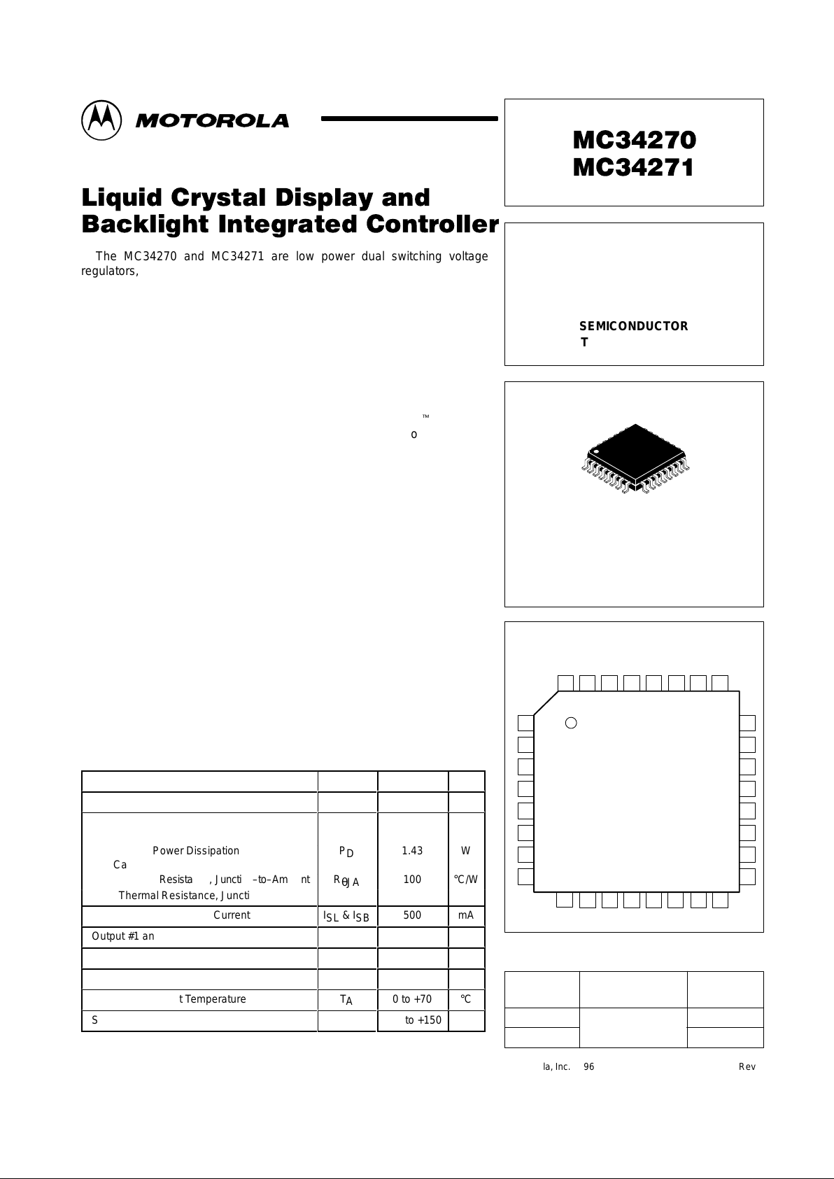
ORDERING INFORMATION
MC34270FB
MC34271FB
TA = 0° to +70°C
QFP–32
QFP–32
FB SUFFIX
PLASTIC PACKAGE
CASE 873
1
32
PIN CONNECTIONS
Order this document by MC34270/D
32
DS
1
Ref
1
FB
1
Comp
1
SS
1
S
1
D
1
Drv
1
DS
2
Ref
2
FB
2
Comp
2
SS
2
S
2
D
2
V
B
SW
Sync
R
Gnd
V
T
A
V
ref
ELD
Mode
V
V
DD
3
V
4
V2V1V
0
1
EN
1
31 30 29 2728 26 25
124
23
22
21
20
19
18
17
2
3
4
5
6
7
8
9101112 1413 15 16
1
MOTOROLA ANALOG IC DEVICE DATA
The MC34270 and MC34271 are low power dual switching voltage
regulators, specifically designed for handheld and laptop applications, to
provide several regulated output voltages using a minimum of external parts.
Two uncommitted switching regulators feature a very low standby bias
current of 5.0 µA, and an operating current of 7.0 mA capable of supplying
output currents in excess of 200 mA.
Both devices have three additional features. The first is an ELD Output
that can be used to drive a backlight or a liquid crystal display. The ELD
output frequency is the clock divided by 256. The second feature allows
four additional output bias voltages, in specific proportions to VB, one of the
switching regulated output voltages. It allows use of mixed logic circuitry and
provides a voltage bias for N–Channel load control MOSFETst. The third
feature is an Enable input that allows a logic level signal to turn–“off” or
turn–“on” both switching regulators.
Due to the low bias current specifications, these devices are ideally suited
for battery powered computer, consumer , and industrial equipment where an
extension of useful battery life is desirable.
MC34270 and MC34271 Features:
• Low Standby Bias Current of 5.0 µA
• Uncommitted Switching Regulators Allow Both Positive and Negative
Supply Voltages
• Logic Enable Allows Microprocessor Control of All Outputs
• Synchronizable to External Clock
• Mode Commandable for ELD and LCD Interface
• Frequency Synchronizable
• Auxiliary Output Bias Voltages Enable Load Control via N–Channel FETs
MOSFET is a trademark of Motorola, Inc.
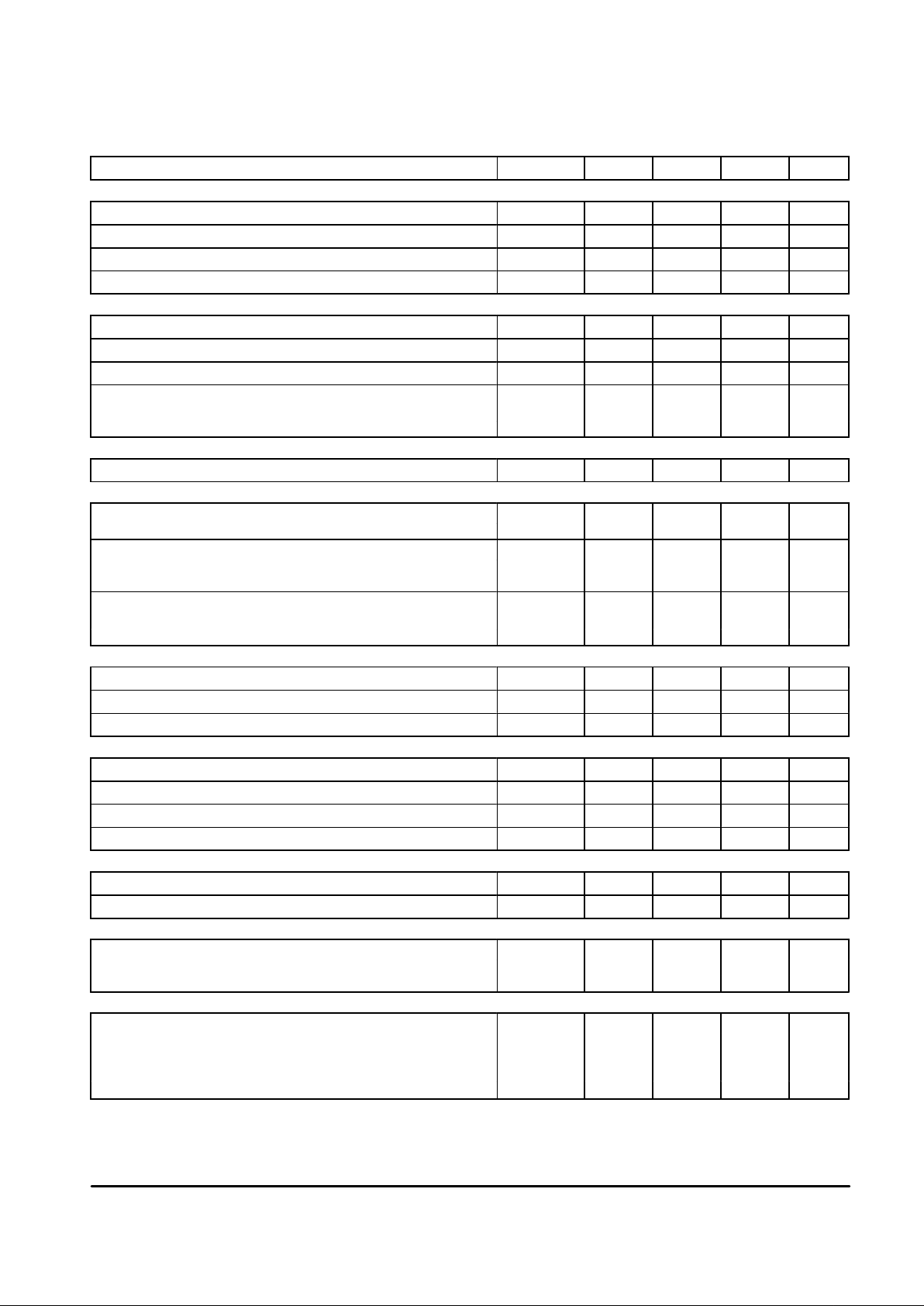
MAXIMUM RATINGS (T
A
= 25°C, unless otherwise noted.)
Rating Symbol Value Unit
Input Voltage
V
DD
ÁÁÁÁ
16
Vdc
БББББББББББ
Á
Power Dissipation and
Thermal Characteristics
ÁÁ
Á
ÁÁÁÁ
ÁÁÁÁÁ
Á
Maximum Power Dissipation P
D
1.43 W
Case 873
Thermal Resistance, Junction–to–Ambient R
θJA
100 °C/W
Thermal Resistance, Junction–to–Case R
θJC
60 °C/W
Output #1 and #2 Switch Current
ISL & I
SB
500
mA
Output #1 and #2 “Off”–State V oltage
V
SL
60
Vdc
Feedback Enable MOSFETs “Off”–State Voltage
V
LF
20
Vdc
Operating Junction Temperature
T
J
125
°C
Operating Ambient Temperature
T
A
0 to +70
°C
БББББББББББ
Storage Temperature Range
ÁÁ
T
stg
ÁÁÁ
–55 to +150Á°C
Motorola, Inc. 1996 Rev 1
Page 2
MC34270 MC34271
2
MOTOROLA ANALOG IC DEVICE DATA
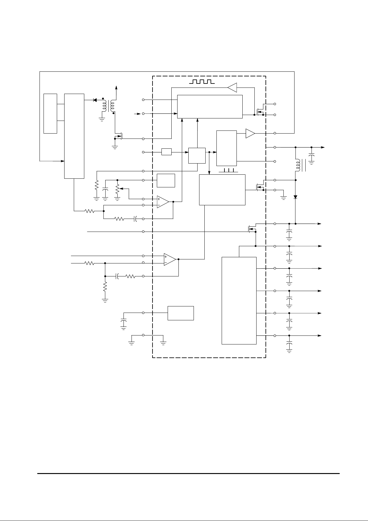
Representative Block Diagram
This device contains 350 active transistors.
V
in
D
1
S
1
SW
1
Sync
Drv
1
EN
1
ELD
Mode
R
T
V
ref
1.25 V
Ref
1
FB
1
V
DD
Comp
1
OSC
D
2
S
2
V
B
V
0
V
1
V
2
V
3
V
4
Ref
2
FB
2
Comp
2
VA = 5.0 V
Gnd
BIAS
V
B
V
2
V
3
V
4
16
15
14
13
12
19
18
17
10
11
9
6
7
32
26
8
31
30
27
2
3
4
23
22
21
28
29
On/Off
From DAC
÷
2
V
1
V
0
BIAS Output
Buffers
V
B
25
µ
P Control
EL
Control
EL
Panel
V
in
EN
2
V
DD
Circuit #1
PWM
Circuit #2
PWM
ELD
EN
V
Ref
V
DD
Page 3
MC34270 MC34271
3
MOTOROLA ANALOG IC DEVICE DATA
ELECTRICAL CHARACTERISTICS (V
DD
= 6.0 V , for typical values TA = Low to High [Note 1], for min/max values TA is
the operating ambient temperature range that applies, unless otherwise noted.)
Characteristic
Symbol Min Typ Max Unit
REFERENCE SECTION
Reference Voltage (TJ = 25°C) V
ref
1.225 1.250 1.275 V
Line Regulation (VDD = 5.0 V to 12.5 V) Reg
line
– 2.0 10 mV
Load Regulation (IO = 0 to 120 µA) Reg
load
– 2.0 10 mV
Total Variation (Line, Load and Temperature) V
ref
1.215 – 1.285 V
ERROR AMPLIFIERS
Input Offset Voltage (VCM = 1.25 V) V
IO
– 1.0 10 mV
Input Bias Current (VCM = 1.25 V) I
IB
– 120 600 nA
Open Loop Voltage Gain (VCM = 1.25 V , V
COMP
= 2.0 V) A
VOL
80 100 – dB
Output Voltage Swing V
High State (IOH = –100 µA) Ve
OH
VA–1.5 4.0 5.5
Low State (IOL = 100 µA) Ve
OL
0 – 1.0
BIAS VOLTAGE
Voltage (VDD = 5.0 V to 12.5 V, IO = 0) V
A
4.6 5.0 5.4 V
OSCILLATOR AND PWM SECTIONS
Total Frequency Variation Over Line and Temperature f
OSC
kHz
VDD = 5.0 V to 10 V, TA = 0° to 70°C, RT = 169 k 90 115 140
Duty Cycle at Each Output %
Maximum DC
max
92 95 –
Minimum DC
min
– – 0
Sync Input
Input Resistance (V
sync
= 3.5 V) R
sync
25 50 100 kΩ
Minimum Sync Pulse Width T
p
– 1.0 – µs
OUTPUT MOSFETs
Output Voltage – “On”–State (I
sink
= 200 mA) V
OL
– 150 250 mV
Output Current – “Off”–State (VOH = 40 V) I
OH
– 0.1 1.0 µA
Rise and Fall Times tr, t
f
– 50 – ns
EL DISCHARGE OUTPUT (ELD) AND DRV
1
Output Voltage – “On”–State (I
sink
= 100 µA) V
OL
– 30 100 mV
Output Voltage – “On”–State (I
sink
= 50 mA) V
OL
– 2.0 2.5 V
Output Voltage – “Off”–State (I
source
= –100 µA) V
OH
VDD–0.5 5.9 – V
Output Voltage – “Off”–State (I
source
= –50 mA) V
OH
VDD–3.5 3.3 – V
FEEDBACK ENABLE SWITCHES (DS1, DS2)
Output Voltage – “Low”–State (I
sink
= 1.0 mA) Vfe
OL
– 10 100 mV
Output Current – “Off”–State (VOH = 12.5 V) Ife
OH
– 0.6 1.0 µA
SWITCHED VDD OUTPUT (SW1)
Output Voltage V
Switch “On” (EN1 = 1, I
source
= 100 µA) Vsw
OH
5.5 5.9 6.0
Switch “Off” (EN1 = 0, I
sink
= 100 µA) Vsw
OL
0 0.1 0.2
AUXILIARY VOLTAGE OUTPUTS
V0 Enable Switch
“On”–Resistance: VB to V
0
Rds 0 2.0 10 Ω
“Off”–State Leakage Current (VB = 10 V) I
lkg
0 0.1 2.0 µA
V0 Voltage (VB = 30 V, I
source
= 0 mA) V
0
29.5 29.9 30 V
V0 Resistance (I
source
= 4.0 mA) R
0
20 40 60 Ω
NOTE: 1. Low duty pulse techniques are used during test to maintain junction temperature as close to ambient as possible.
Page 4
MC34270 MC34271
4
MOTOROLA ANALOG IC DEVICE DATA
ELECTRICAL CHARACTERISTICS
(continued) (VDD = 6.0 V , for typical values TA = Low to High [Note 1], for min/max values TA is
the operating ambient temperature range that applies, unless otherwise noted.)
Characteristic UnitMaxTypMinSymbol
AUXILIARY VOLTAGE OUTPUTS
V1, V2, V3, V4 Outputs
1–V1/V0 Ratio: MC34270 0.0565 0.0580 0.0595
MC34271 0.0500 0.0520 0.0535
1–V2/V0 Ratio: MC34270 0.1135 0.1160 0.1185
MC34271 0.1010 0.1035 0.1065
V3/V0 Ratio: MC34270 0.1135 0.1 160 0.1 185
MC34271 0.1010 0.1035 0.1065
V4/V0 Ratio: MC34270 0.0565 0.0580 0.0595
MC34271 0.0500 0.0520 0.0535
Output Resistance (I
source
= 4.0 mA) R
o
20 40 60 Ω
Output Short Circuit Current I
ss
5.0 10 20 mA
LOGIC INPUTS (EN1, EN2, MODE)
Input Low State V
IL
0 – 0.8 V
Input High State V
IH
2.0 – 6.0 V
Input Impedance R
in
25 50 100 kΩ
SOFT START CONTROL (SS1,SS2)
Charge Current (Capacitor Voltage = 1.0 V to 4.0 V)
I
chg
0.5 1.0 2.5 µA
Discharge Current (Capacitor Voltage = 1.0 V) I
dschg
250 650 – µA
TOTAL SUPPLY CURRENT
VDD Current VDD = 6.0 V I
CC
– 2.0 5.0 µA
Standby Mode (EN1 = EN2 = 0) VDD = 16 V – 3.0 15
VDD Current I
CC
– 0.7 3.0 mA
Backlight “On” (EN1 = 1; EN2 = 0)
VDD Current I
CC
– 0.9 2.0 mA
LCD “On” (No Inductor) (EN1 = 0; EN2 = 1)
VB Current (V0 = 35 V) I
O
– 1.2 3.0 mA
NOTE: 1. Low duty pulse techniques are used during test to maintain junction temperature as close to ambient as possible.
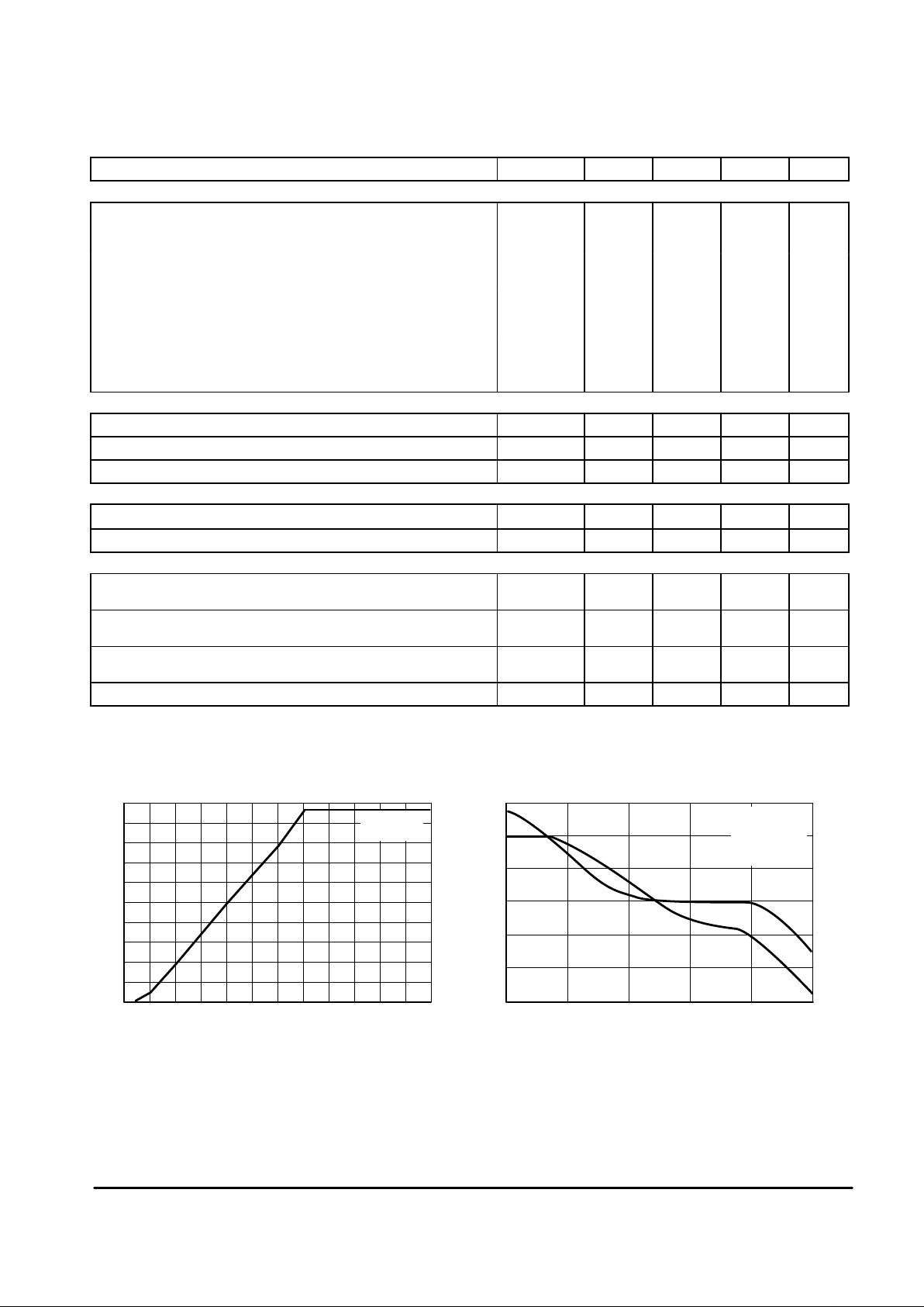
10
100
1.5
1.0
A
VOL
, OPEN LOOP VOL TAGE GAIN (dB)
f, FREQUENCY (Hz)
DC, SWITCH OUTPUT DUTY CYCLE
Figure 1. Switch Output Duty Cycle versus
Compensation Voltage
V
Comp
, COMPENSATION VOLTAGE (V)
Figure 2. Error Amp Open Loop Gain and
Phase versus Frequency
0.6
0.4
0.2
0
0.8
80
60
40
20
0
–20
2.0 2.5 3.0 3.5 4.0 4.5 100 1.0 k 10 k 100 k 1000 k
θ
, EXCESS PHASE ( )
90
120
150
180
°
VDD = 6.0 V
TA = 25
°
C
VDD = 6.0 V
V
Comp
= 2.5 V
RL = Open
TA = 25
°
C
0
30
60
Gain
Phase
Page 5

MC34270 MC34271
5
MOTOROLA ANALOG IC DEVICE DATA
0
0
2.0
2.5
0
0.16
0
0
V
sat
, SWITCH OUTPUT SOURCE SA TURATION (V)
I
Source
, SWITCH OUTPUT CURRENT (mA)
QUIESCENT CURRENT (mA)
VDD, SUPPLY VOLTAGE (V)
FET DRAIN VOLTAGE (V)
ID, DRAIN CURRENT (mA)
OUTPUT VOLTAGE DROP (mV)
I, CURRENT DRAW (mA)
Figure 3. Reference Voltage Change versus
Reference Current
Figure 4. Quiescent Current versus Supply Voltage
Figure 5. FET Drain Voltage versus Sink Current
Figure 6. ELD and DRV1 Switch Output Source
and Sink Saturation versus Current
VDD = 6.0 V
TA = 25
°
C
VDD = 6.0 V
TA = 25
°
C
V
DD
Source Saturation
V
ref
V
A
EN1 and EN2 = 1
EN1 = 1 and EN2 = 0
RT = 169 k
No Loading
TA = 25
°
C
Standby Current
EN1 and EN2 = 0
Sink Saturation
1.5
2.0
1.0
0.5
0
– 5.0
–10
–15
–20
–25
–30
0.12
0.08
0.04
–1.0
– 2.0
– 3.0
30 6015 4550 150100 200
1.0 2.0 3.0 4.0 5.0 4.0 6.0 8.0 10 12 16 18
2.0
2.2
V
sat
, SWITCH OUTPUT SINK SA TURATION (V)
µ
STANDBY SUPPLY CURRENT ( A)
1.4
1.8
1.0
0.6
0.2
1.5
1.0
0.5
14
0 – 4.0 0
VDD = 6.0 V
TA = 25
°
C
TA, AMBIENT TEMPERATURE (°C)
0
8.0
0
0.30
OSCILLAT OR FREQUENCY CHANGE (kHz)
VOLTAGE VARIATION (V)
Figure 7. V
ref
and VA Variation
versus Temperature
TA, AMBIENT TEMPERATURE (°C)
Figure 8. Oscillator Frequency Variation
versus Temperature
0.25
0.20
0.15
0.10
0.05
0
– 0.05
– 0.10
6.0
4.0
2.0
0
– 2.0
– 4.0
– 6.0
– 8.0
10 20 30 40 50 60 70 10 20 30 40 50 60 70
VDD = 6.0 V
RT = 169 k
VDD = 6.0 V
V
ref
V
A
Page 6

MC34270 MC34271
6
MOTOROLA ANALOG IC DEVICE DATA
VDD LEVEL (V)
00
1000
REFERENCE VOLTAGE (V)
FREQUENCY (kHz)
Figure 9. Frequency versus Timing
TIMING RESISTANCE (kΩ, s)
Figure 10. VA, V
ref
versus V
DD
100
10
5.0
4.0
3.0
2.0
1.0
0
100 1000 1.0 2.0 3.0 4.0 5.0 6.0
VDD = 6.0 V
TA = 25
°
C
RT = 169 k
TA = 25
°
C
V
A
V
ref
OPERA TING DESCRIPTION
The MC34270 and MC34271 series are monolithic, fixed
frequency power switching regulators specifically designed
for dc to dc converter and battery powered applications.
These devices operate as fixed frequency, voltage mode
regulators containing all the active functions required to
directly implement step–up, step–down and voltage inverting
converters with a minimum number of external components.
Potential markets include battery powered, handheld,
automotive, computer, industrial and cost sensitive consumer
products. A description of each section is given below with
the representative block diagram shown in Figure 9.
Oscillator
The oscillator frequency is programmed by resistor RT.
The charge to discharge ratio is controlled to yield a 95%
maximum duty cycle at the switch outputs. During the fall
time of the internal sawtooth waveform, the oscillator
generates an internal blanking pulse that holds the inverting
input of the AND gates high, disabling the output switching
MOSFETs. The internal sawtooth waveform has a nominal
peak voltage of 3.3 V and a valley voltage of 1.7 V.
Pulse Width Modulators
Both pulse width modulators consist of a comparator with
the oscillator ramp voltage applied to the noninverting input,
while the error amplifier output is applied to the inverting
input. A third input to the comparator has a 0.5 mA typical
current source that can be used to implement soft start.
Output switch conduction is initiated when the ramp
waveform is discharged to the valley voltage. As the ramp
voltage increases to a voltage that exceeds the error
amplifier output, the latch resets, terminating output
MOSFET conduction for the duration of the oscillator ramp.
This PWM/latch combination prevents multiple output pulses
during a given oscillator cycle.
Each PWM circuit is enabled by a logic input. When
disabled, the entire block is turned off, drawing only leakage
current from the power source. Shared circuits, like the
reference and oscillator, can be activated by either EN
1
or EN2.
Circuit #1 has an ELD output which may be used to drive
an LCD or backlight. Its output frequency is the oscillator
frequency divided by 1024.
Error Amplifiers and Reference
Each error amplifier is provided with access to both
inverting and noninverting inputs, and the output. The Error
Amplifiers’ Common Mode Input Range is 0 to 2.5 V. The
amplifiers have a minimum dc voltage gain of 60 dB. The
1.25 V reference has an accuracy of ±4.0% at room
temperature.
External loop compensation is required for converter
stability. A simple low–pass filter is formed by connecting a
resistive divider from the output to the error amplifier
inverting input, and a series resistor–capacitor from the error
amplifier output also to the to the inverting input. The step
down converter is easiest to compensate for stability. The
step–up and voltage inverting configurations, when operated
as continuous conduction boost or flyback converters, are
more difficult to compensate, and may require a lower loop
design bandwidth.
MOSFET Switch Outputs
The output MOSFETs are designed to switch a maximum
of 60 V, with a peak drain current capability of 500 mA. In
circuit #1 an additional DRV1 output is provided for
interfacing with an external MOSFET.The gates of the
MOSFETs are held low when the circuit is disabled.
Auxiliary Output Voltages
Output voltages V0 through V4 are provided for use as
references or bias voltages. V0 is the circuit #2 output
voltage, when an internal FET switch is activated. The other
auxiliary output voltages are proportional to VB. The
amplifiers for V1 and V2 are powered from V0, while the
amplifiers for V3 and V4 are powered from VDD.
Page 7

MC34270 MC34271
7
MOTOROLA ANALOG IC DEVICE DATA
Figure 11. Representative Block Diagram Electroluminescent Backlight Configuration
En
R
S
Q
V
DD
D
1
S
1
DS
1
SW
1
Sync
Drv
1
EN
1
ELD
Mode
R
S
Q
R
T
SS
1
V
ref
1.25 V
Ref
1
FB
1
Circuit #1 Bias Supply
V
DD
V
DD
Comp
1
En
OSC
D
2
S
2
V
B
V
0
V
1
V
2
V
3
V
4
V
DD
Circuit #2
Bias Supply
Ref
2
FB
2
Comp
2
SS
2
DS
2
EN
2
V
A
Gnd
BIAS
V
B
6.0 V to 30 V
V
2
V
3
V
4
V
DD2
V
DD2
V
DD2
169 k
16
15
14
13
12
19
18
17
10
11
9
6
7
32
1
26
8
31
30
27
2
3
4
5
23
22
21
20
24
25
28
29
EL
Panel
Brightness
“On/Off”
LCD
Display
DAC
÷
2
÷
N
V
1
V
0
V
B
Page 8

MC34270 MC34271
8
MOTOROLA ANALOG IC DEVICE DATA
Figure 12. Auxiliary Supply Configuration
En
R
S
Q
V
DD
5.0 V to 16 V
D
1
S
1
DS
1
SW
1
Sync
Drv
1
EN
1
ELD
Mode
R
S
Q
R
T
SS
1
V
ref
1.25 V
Ref
1
FB
1
Circuit #1 Bias Supply
V
DD
V
DD
Comp
1
En
OSC
D
2
S
2
V
B
V
0
V
1
V
2
V
3
V
4
V
DD
Circuit #2
Bias Supply
Ref
2
FB
2
Comp
2
SS
2
DS
2
EN
2
V
A
Gnd
BIAS
V
B
6.0 V to 30 V
V
2
V
3
V
4
V
DD2
V
DD2
V
DD2
169 k
16
15
14
13
12
19
18
17
10
11
9
6
7
32
1
26
8
31
30
27
2
3
4
5
23
22
21
20
24
25
28
29
LCD
Display
÷
2
÷
N
V
1
V
0
LCD
Contrast
–27 V
V
B
12 V
12 V
DAC
Page 9

MC34270 MC34271
9
MOTOROLA ANALOG IC DEVICE DATA
Figure 13. MC34270 Incandescent Backlight Configuration
En
R
S
Q
V
in
5.0 V to 16 V
D
1
S
1
DS
1
SW
1
Sync
Drv
1
EN
1
ELD
Mode
R
S
Q
R
T
SS
1
V
ref
1.25 V
Ref
1
FB
1
Circuit #1 Bias Supply
V
DD
V
DD
Comp
1
En
OSC
D
2
S
2
V
B
V
0
V
1
V
2
V
3
V
4
V
DD
Circuit #2
Bias Supply
Ref
2
FB
2
Comp
2
SS
2
DS
2
EN
2
V
A
Gnd
BIAS
6.0 V to 30 V
V
2
V
3
V
4
V
DD2
V
DD2
V
DD2
169 k
16
15
14
13
12
19
18
17
10
11
9
6
7
32
1
26
8
31
30
27
2
3
4
5
23
22
21
20
24
25
28
29
LCD
Display
÷
2
÷
N
V
1
V
0
LCD
Contrast
V
ref
DS
1
1
0.1 µF
MC34270
DAC
Page 10

MC34270 MC34271
10
MOTOROLA ANALOG IC DEVICE DATA
Figure 14. EL PANEL Drive Circuit
R
S
Q
Vin 6.0 V
D
1
S
1
SW
1
Sync
Drv
1
EN
1
ELD
Mode
R
S
Q
R
T
SS
1
V
ref
1.25 V
Ref
1
FB
1
Circuit #1 Bias Supply
V
DD
V
DD
Comp
1
En
OSC
D
2
S
2
V
B
V
0
V
1
V
2
V
3
V
4
V
DD
Circuit #2
Bias Supply
Ref
2
FB
2
Comp
2
SS
2
DS
2
EN
2
V
A
Gnd
BIAS
V
B
V
2
V
3
V
4
V
DD2
V
DD2
V
DD2
160 k
16
15
14
13
12
19
18
17
10
11
9
6
7
32
26
8
31
30
27
2
3
4
5
23
22
21
20
24
25
28
29
LCD
Display
÷
2
÷
N
V
1
V
0
V
ref
DS
1
1
MC34270 or MC34271
DAC
V
B
EL
PANEL
2.2 M
8.25 k
9.1 k
0.1
µ
F
4.3 M
15 pF
0.1 µF
8.2 k
1.0 k
400 Hz
0.1
µ
F
10
2.2 k
MTP3055EL
MR856
10
µ
F
4T
#364T#36
65
34
MR856
8
7
0.22 µF
200 V
120T
#36
2
1
15 k
1.0 k
NOTES::1. Transformer information TDK Core # PC40EEM12.7/13.7–Z
Bobbin # BEPC–10–118G 2 mil gap. LP = 1.6 µhy.
2.EL PANEL: DUREL 3/SL ORANGE
+
MPSA44
120T
#36
10 k
1.0 k
22 k
MMBT2907
Page 11

MC34270 MC34271
11
MOTOROLA ANALOG IC DEVICE DATA
FB SUFFIX
PLASTIC PACKAGE
CASE 873–01
0.274
0.274
0.055
0.010
0.051
0.010
–
0.005
0.013
6
°
0.005
5
°
0.006
0.348
0.006
5
°
0.348
MIN MINMAX MAX
MILLIMETERS INCHES
DIM
7.10
7.10
1.60
0.373
1.50
–
0.20
0.197
0.57
8
°
0.135
10
°
0.25
9.15
0.25
11
°
9.15
6.95
6.95
1.40
0.273
1.30
0.273
–
0.119
0.33
6
°
0.119
5
°
0.15
8.85
0.15
5
°
8.85
0.031 BSC
0.220 REF
0.016 BSC
0.80 BSC
5.6 REF
0.40 BSC
A
B
C
D
E
F
G
H
J
K
L
M
N
P
Q
R
S
T
U
V
X
0.280
0.280
0.063
0.015
0.059
–
0.008
0.008
0.022
8
°
0.005
10
°
0.010
0.360
0.010
11
°
0.360
NOTES:
1. DIMENSIONING AND TOLERANCING PER ANSI
Y14.5M, 1982.
2. CONTROLLING DIMENSION: MILLIMETER.
3. DATUM PLANE –H– IS LOCATED AT BOTTOM OF
LEAD AND IS COINCIDENT WITH THE LEAD WHERE
THE LEAD EXITS THE PLASTIC BODY AT THE
BOTTOM OF THE PARTING LINE.
4. DATUMS –A–, –B– AND –D– TO BE DETERMINED AT
DATUM PLANE –H–.
5. DIMENSIONS S AND V TO BE DETERMINED AT
SEATING PLANE –C–.
6. DIMENSIONS A AND B DO NOT INCLUDE MOLD
PROTRUSION. ALLOWABLE PROTRUSION IS 0.25
(0.010) PER SIDE. DIMENSIONS A AND B DO
INCLUDE MOLD MISMATCH AND ARE DETERMINED
AT DATUM PLANE –H–.
7. DIMENSION D DOES NOT INCLUDE DAMBAR
PROTRUSION. ALLOWABLE DAMBAR PROTRUSION
SHALL BE 0.08 (0.003) TOTAL IN EXCESS OF THE D
DIMENSION AT MAXIMUM MA TERIAL CONDITION.
DAMBAR CANNOT BE LOCATED ON THE LOWER
RADIUS OR THE FOOT.
–H–
DATUM
PLANE
X
K
DETAIL C
U
T
R
Q
P
DETAIL A
–A–,–B–,–D–
B
B
J
BASE METAL
D
N
SECTION B–B
VIEW ROTATED 90° CLOCKWISE
F
–H–
DATUM
PLANE
H
32
25
24 17
16
9
81
V
B
–B–
L
–A–
L
–D–
A
S
DETAIL A
–C–
SEATING
PLANE
C
E
DETAIL C
M
M
G
1.0 REF 0.039 REF
C
0.20 (0.008) A–B D
S S
M
0.01
(0.004)
H
0.20 (0.008) A–B D
S S
M
C
0.20 (0.008) A–B D
A–B
0.05 (0.002)
S S
M
0.20 (0.008) C A–B D
0.05 (0.002) A–B
M
S S
0.20 (0.008) H A–B D
M
S S
OUTLINE DIMENSIONS
Page 12

MC34270 MC34271
12
MOTOROLA ANALOG IC DEVICE DATA
Motorola reserves the right to make changes without further notice to any products herein. Motorola makes no warranty , representation or guarantee regarding
the suitability of its products for any particular purpose, nor does Motorola assume any liability arising out of the application or use of any product or circuit, and
specifically disclaims any and all liability, including without limitation consequential or incidental damages. “T ypical” parameters which may be provided in Motorola
data sheets and/or specifications can and do vary in different applications and actual performance may vary over time. All operating parameters, including “Typicals”
must be validated for each customer application by customer’s technical experts. Motorola does not convey any license under its patent rights nor the rights of
others. Motorola products are not designed, intended, or authorized for use as components in systems intended for surgical implant into the body, or other
applications intended to support or sustain life, or for any other application in which the failure of the Motorola product could create a situation where personal injury
or death may occur. Should Buyer purchase or use Motorola products for any such unintended or unauthorized application, Buyer shall indemnify and hold Motorola
and its officers, employees, subsidiaries, affiliates, and distributors harmless against all claims, costs, damages, and expenses, and reasonable attorney fees
arising out of, directly or indirectly, any claim of personal injury or death associated with such unintended or unauthorized use, even if such claim alleges that
Motorola was negligent regarding the design or manufacture of the part. Motorola and are registered trademarks of Motorola, Inc. Motorola, Inc. is an Equal
Opportunity/Affirmative Action Employer.
How to reach us:
USA/EUROPE/ Locations Not Listed: Motorola Literature Distribution; JAPAN: Nippon Motorola Ltd.; Tatsumi–SPD–JLDC, 6F Seibu–Butsuryu–Center,
P.O. Box 20912; Phoenix, Arizona 85036. 1–800–441–2447 or 602–303–5454 3–14–2 Tatsumi Koto–Ku, Tokyo 135, Japan. 03–81–3521–8315
MFAX: RMF AX0@email.sps.mot.com – TOUCHT ONE 602–244–6609 ASIA/PACIFIC: Motorola Semiconductors H.K. Ltd.; 8B Tai Ping Industrial Park,
INTERNET: http://Design–NET.com 51 Ting Ko k Road, Tai Po, N.T ., Hong Kong. 852–26629298
MC34270/D
*MC34270/D*
◊
 Loading...