

Page 1
The MC34261/MC33261 are active power factor controllers specifically
designed for use as a preconverter in electronic ballast and in off–line power
converter applications. These integrated circuits feature an internal startup
timer, a one quadrant multiplier for near unity power factor, zero current
detector to ensure critical conduction operation, high gain error amplifier,
trimmed internal bandgap reference, current sensing comparator, and a
totem pole output ideally suited for driving a power MOSFET.
Also included are protective features consisting of input undervoltage
lockout with hysteresis, cycle–by–cycle current limiting, and a latch for single
pulse metering. These devices are available in dual–in–line and surface
mount plastic packages.
• Internal Startup Timer
• One Quadrant Multiplier
• Zero Current Detector
• Trimmed 2% Internal Bandgap Reference
• Totem Pole Output
• Undervoltage Lockout with Hysteresis
• Low Startup and Operating Current
• Pinout Equivalent to the SG3561
• Functional Equivalent to the TDA4817
Order this document by MC34261/D
POWER FACTOR
CONTROLLERS
SEMICONDUCTOR
TECHNICAL DATA
P SUFFIX
PLASTIC PACKAGE
8
1
8
1
CASE 626
D SUFFIX
PLASTIC PACKAGE
CASE 751
(SO–8)
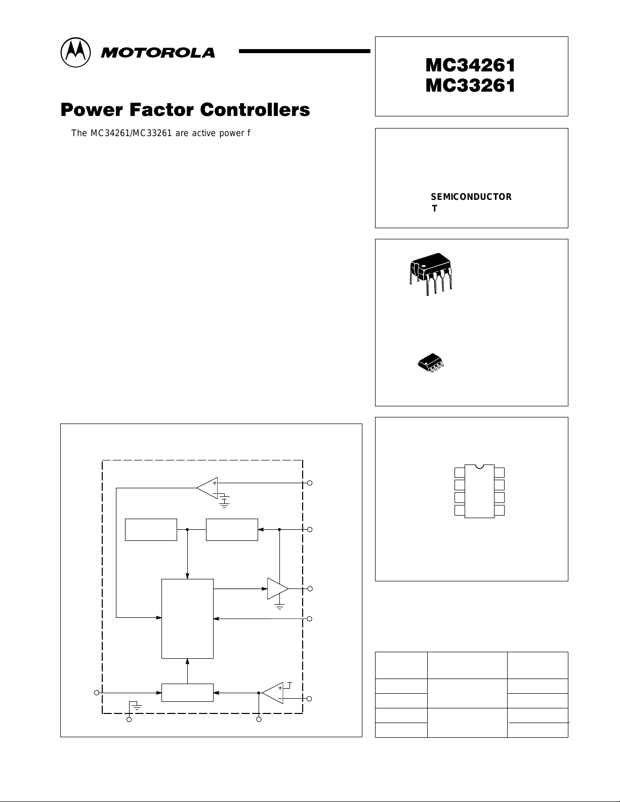
Multiplier
Input
Simplified Block Diagram
PIN CONNECTIONS
Voltage Feedback
Zero Current Detector
&
Undervoltage
Lockout
Error Amp
Compensation
V
2
2.5V
Reference
Multiplier,
Latch,
PWM,
Timer,
Logic
3
6
Gnd
Multiplier
ref
Zero Current
Detect Input
5
V
CC
8
Drive Output
7
Current Sense
Input
4
Voltage
Feedback
1
Input
Compensation
Multiplier Input
Current Sense
ORDERING INFORMATION
Device
MC34261D
MC34261P
MC33261D
MC33261P
1
Input
2
3
4
Input
(Top View)
Operating
Temperature Range
TA = 0° to +70°C
TA = –40° to +85°C
V
8
CC
Drive Output
7
Gnd
6
Zero Current
5
Detect Input
Package
Plastic DIP
Plastic DIP
SO–8
SO–8
MOTOROLA ANALOG IC DEVICE DATA
Motorola, Inc. 1996 Rev 1
1
Page 2

MC34261 MC33261
MAXIMUM RATINGS
Rating Symbol Value Unit
Total Power Supply and Zener Current (ICC + IZ) 30 mA
Output Current, Source or Sink (Note 1) I
Current Sense, Multiplier, and V oltage Feedback Inputs V
Zero Current Detect Input
High State Forward Current
Low State Reverse Current
Power Dissipation and Thermal Characteristics
P Suffix, Plastic Package Case 626
Maximum Power Dissipation @ TA = 70°C
Thermal Resistance, Junction–to–Air
R
D Suffix, Plastic Package Case 626
Maximum Power Dissipation @ TA = 70°C
Thermal Resistance, Junction–to–Air
R
Operating Junction Temperature T
Operating Ambient Temperature (Note 3)
MC34261
MC33261
Storage Temperature T
O
I
in
P
θJA
P
θJA
T
stg
in
D
D
J
A
500 mA
–1.0 to 10 V
50
–10
800
100
450
178
+150 °C
0 to +70
–40 to +85
–55 to +150 °C
mA
mW
°C/W
mW
°C/W
°C
ELECTRICAL CHARACTERISTICS (V
= 12 V, for typical values TA = 25°C, for min/max values TA is the operating ambient
CC
temperature range that applies [Note 3], unless otherwise noted.)
Characteristic
Symbol Min Typ Max Unit
ERROR AMPLIFIER
Voltage Feedback Input Threshold
TA = 25°C
TA = T
low
to T
(VCC = 12 V to 28 V)
high
Line Regulation (VCC = 12 V to 28 V, TA = 25°C) Reg
Input Bias Current (VFB = 0 V) I
Open Loop Voltage Gain A
V
FB
IB
VOL
line
2.465
2.44
2.5 2.535
2.54
– 1.0 10 mV
– –0.3 –1.0 µA
65 85 – dB
Gain Bandwidth Product (TA = 25°C) GBW 0.7 1.0 – MHz
Output Source Current (VO = 4.0 V, VFB = 2.3 V) I
Source
0.25 0.5 0.75 mA
Output Voltage Swing
High State (I
Low State (I
= 0.2 mA, VFB = 2.3 V)
Source
= 0.4 mA, VFB = 2.7 V)
Sink
V
OH
V
OL
5.0
–
2.1
5.7
–
2.44
MULTIPLIER
Dynamic Input Voltage Range
Multiplier Input (Pin 3)
Compensation (Pin 2)
Input Bias Current (VFB = 0 V) I
Multiplier Gain (V
Pin 3
= 0.5 V, V
= VFB + 1.0 V) (Note 2) K 0.4 0.62 0.8 1/V
Pin 2
V
V
Pin 3
Pin 2
IB
0 to 2.5
VFB to
(VFB + 1.0)
0 to 3.5
VFB to
(VFB + 1.5)
–
–
– –0.3 –1.0 µA
ZERO CURRENT DETECTOR
Input Threshold Voltage (Vin Increasing) V
Hysteresis (Vin Decreasing) V
th
H
1.3 1.6 1.8 V
40 110 200 mV
Input Clamp Voltage
High State (I
Low State (I
NOTES: 1. Maximum package power dissipation limits must be observed.
2. K =
3. T
low
3. T
low
= 3.0 mA)
DET
= –3.0 mA)
DET
Pin 4 Threshold Voltage
V
Pin 3(VPin 2
= –40°C for MC34261
= –40°C for MC33261
– VFB)
T
= +70°C for MC34261
high
T
= +85°C for MC33261
high
V
IH
V
IL
6.1
0.3
6.7
0.7
–
1.0
V
V
V
V
2
MOTOROLA ANALOG IC DEVICE DATA
Page 3
MC34261 MC33261
ELECTRICAL CHARACTERISTICS (V
= 12 V, for typical values TA = 25°C, for min/max values TA is the operating ambient
CC
temperature range that applies [Note 3], unless otherwise noted.)
Characteristic
CURRENT SENSE COMPARATOR
Input Bias Current (V
Input Offset Voltage (V
Delay to Output t
= 0 V) I
Pin 4
Pin 2
= 1.1 V, V
= 0 V) V
Pin 3
PHL (in/out)
DRIVE OUTPUT
Output Voltage (VCC = 12 V)
Low State (I
Low State (I
High State (I
High State (I
Output Voltage (VCC = 30 V)
High State (I
= 20 mA)
Sink
= 200 mA)
Sink
= 20 mA)
Source
= 200 mA)
Source
= 20 mA, CL = 15 pF)
Source
V
Output Voltage Rise T ime (CL = 1.0 nF) t
Output Voltage Fall T ime (CL = 1.0 nF) t
Output Voltage with UVLO Activated (VCC = 7.0 V, I
= 1.0 mA) V
Sink
OH(UVLO)
RESTART TIMER
Restart Time Delay t
UNDERVOLTAGE LOCKOUT
Startup Threshold (VCC Increasing) V
Minimum Operating Voltage After Turn–On (VCC Decreasing) V
Hysteresis V
TOTAL DEVICE
Power Supply Current
Startup (VCC = 7.0 V)
Operating
Dynamic Operating (50 kHz, CL = 1.0 nF)
Power Supply Zener Voltage V
NOTES: 1. Maximum package power dissipation limits must be observed.
Pin 4 Threshold Voltage
2. K =
V
3. T
3. T
Pin 3(VPin 2
= –40°C for MC34261
low
= –40°C for MC33261
low
– VFB)
T
= +70°C for MC34261
high
T
= +85°C for MC33261
high
Symbol Min Typ Max Unit
IB
IO
– –0.5 –2.0 µA
– 3.5 15 mV
– 200 400 ns
V
V
OL
V
OH
O(max)
r
f
–
1.8
9.8
7.8
0.3
2.4
10.3
8.3
0.8
3.3
–
8.8
14 16 18
– 50 120 ns
– 50 120 ns
V
– 0.2 0.8 V
DLY
th
Shutdown
H
I
CC
Z
150 400 – µs
9.2 10.0 10.8 V
7.0 8.0 9.0 V
1.75 2.0 2.5 V
mA
–
–
–
0.3
7.1
9.0
0.5
12
20
30 36 – V
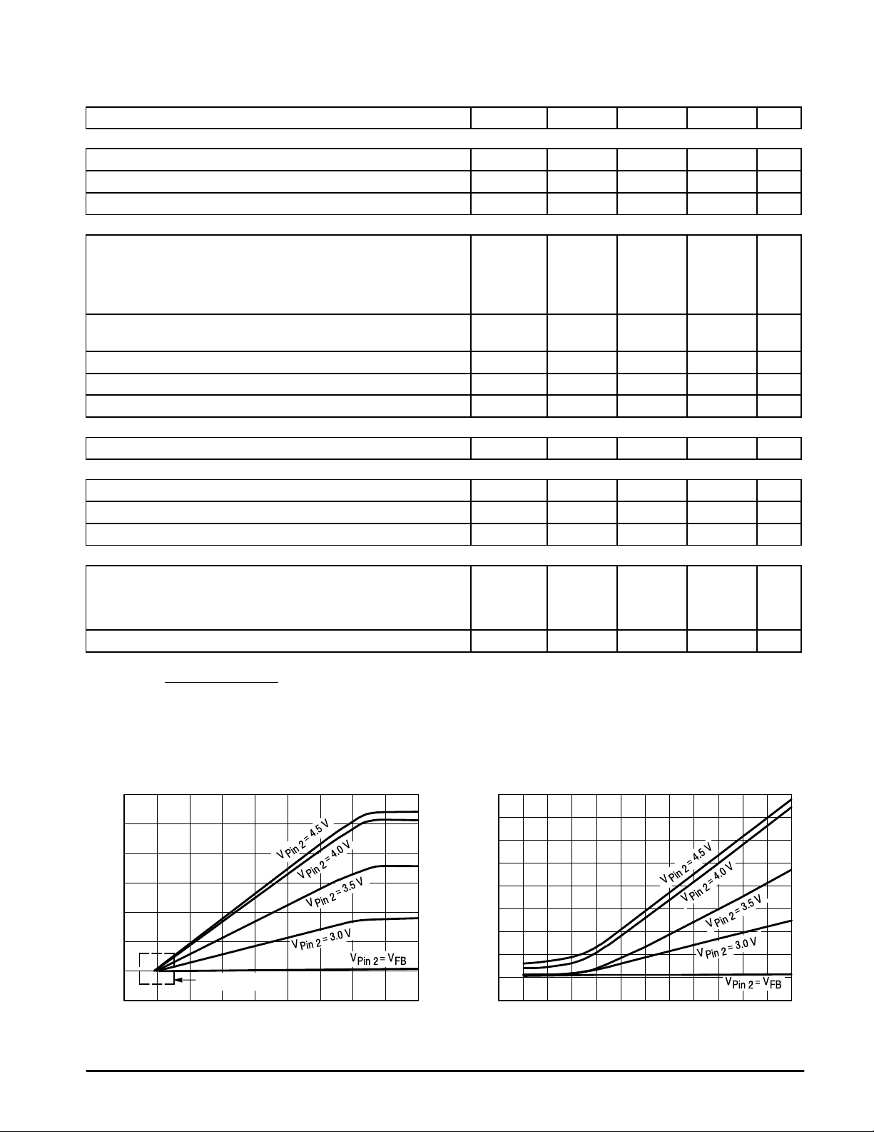
Figure 1. Current Sense Input Threshold
versus Multiplier Input
3.0
2.5
2.0
1.5
1.0
0.5
0
, CURRENT SENSE THRESHOLD VOLTAGE (V)
CS
–0.5
V
–0.5 4.0
See Figure 2
1.0 1.5
VM, MULTIPLIER INPUT VOLTAGE (V)
MOTOROLA ANALOG IC DEVICE DATA
, CURRENT SENSE THRESHOLD VOLTAGE (V)
V
CS
0.16
0.14
0.12
0.10
0.08
0.06
0.04
0.02
–0.02
–0.12
Figure 2. Current Sense Input Threshold
versus Multiplier Input
0
–0.08 0 0.04 0.08 0.120 0.5 2.0 2.5 3.0 3.5 –0.04
VM, MULTIPLIER INPUT VOLTAGE (V)
3
Page 4
MC34261 MC33261
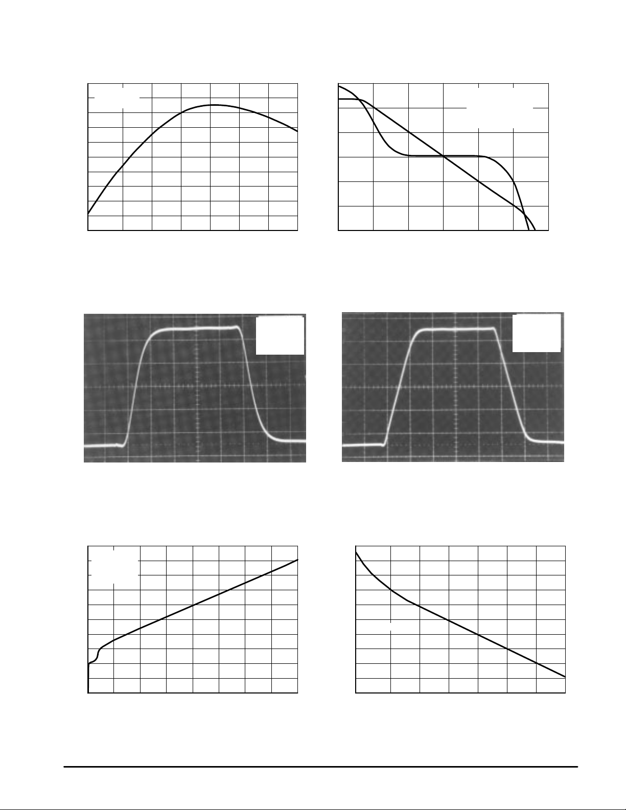
Figure 3. V oltage Feedback Input Threshold
Change versus T emperature
+4.0
VCC = 12 V
Pins 1 to 2
0
–4.0
–8.0
–12
, VOLTAGE FEEDBACK THRESHOLD CHANGE (mV)
FB
–16
V
–55
∆
–25 0 25 50 75 100 125
TA, AMBIENT TEMPERATURE (
Figure 5. Error Amp Small Signal
Transient Response
2.55 V
°
C)
VCC = 12 V
AV = –1.0
°
C
TA = 25
Figure 4. Error Amp Open Loop Gain and
100
80
60
40
20
, OPEN LOOP VOL TAGE GAIN (dB)
0
VOL
A
–20
10
3.0 V
100 1.0 k 10 k 100 k 1.0 M 10 M
Phase versus Frequency
VCC = 12 V
VO = 3.0 V to 3.5 V
Gain
f, FREQUENCY (Hz)
RL = 100 k
°
C
TA = 25
Figure 6. Error Amp Large Signal
Transient Response
VCC = 12 V
Phase
AV = –1.0
°
TA = 25
0
30
°
60
90
120
, EXCESS PHASE ( C)
φ
150
180
C
2.5 V
2.45 V
0.5
µ
Figure 7. Error Amp Output Saturation
versus Sink Current
5.0
VCC = 12 V
VFB = 2.7 V
4.0
3.0
2.0
1.0
, OUTPUT SA TURATION VOLTAGE (V)
sat
V
0
0 0.5 1.0 1.5
TA = 25
°
C
I
, OUTPUT SINK CURRENT (mA)
Sink
s/DIV
2.0
2.5 V
20 mV/DIV
2.0 V
525
µ
475
425
375
, RESTART TIME DELAY ( s)
325
DLY
t
275
1.0 µs/DIV
Figure 8. Restart Time Delay versus Temperature
VCC = 12 V
–55
–25 0 25 50 75 100 125
TA, AMBIENT TEMPERATURE (°C)
200 mV/DIV
4
MOTOROLA ANALOG IC DEVICE DATA
Page 5

MC34261 MC33261
Figure 9. Zero Current Detector Input Threshold
V oltage Change versus Temperature
40
20
Upper Threshold
0
(Vin Increasing)
–20
, THRESHOLD VOLTAGE CHANGE (mV)
th
V
∆
–40
–55 –25 0 25 50 75 100 125
TA, AMBIENT TEMPERATURE (
VCC = 12 V
Lower Threshold
(Vin Decreasing)
°
C)
Figure 11. Drive Output Waveform
90
%
VCC = 12 V
CL = 1.0 nF
TA = 25
Figure 10. Output Saturation Voltage
versus Load Current
0
–2.0
–4.0
–6.0
4.0
2.0
, OUTPUT SA TURATION VOLTAGE (V)
sat
V
0
0 80 160 240 320
Source Saturation
(Load to Ground)
Sink Saturation
(Load to VCC)
V
CC
Gnd
IO, OUTPUT LOAD CURRENT (mA)
VCC = 12 V
µ
s Pulsed Load
80
120 Hz Rate
Figure 12. Drive Output Cross Conduction
VCC = 12 V
°
C
, OUTPUT VOL TAGE
O
CL = 15 pF
°
C
TA = 25
5.0 V/DIV
10
%
100 ns/DIV 100 ns/DIV
Figure 13. Supply Current versus Supply V oltage
16
12
8.0
VFB = 0 V
, SUPPLY CURRENT (mA)
4.0
CC
I
0
0
10 20 30 40
VCC, SUPPLY VOLTAGE (V)
Current Sense = 0 V
Multiplier = 0 V
CL = 1.0 nF
f = 50 kHz
TA = 25
100 mA/DIV
, SUPPLY CURRENT V
CC
I
Figure 14. Undervoltage Lockout Thresholds
versus T emperature
12
11
10
9.0
8.0
, SUPPLY VOLTAGE (V)
CC
V
7.0
°
C
6.0
–55 –25 0 25 50 75 100 125
Startup Threshold
(VCC Increasing)
Minimum Operating Threshold
(VCC Decreasing)
TA, AMBIENT TEMPERATURE (°C)
MOTOROLA ANALOG IC DEVICE DATA
5
Page 6

MC34261 MC33261
FUNCTIONAL DESCRIPTION
Introduction
Most electronic ballasts and switching power supplies use
a bridge rectifier and a filter capacitor to derive raw dc voltage
from the utility ac line. This simple rectifying circuit draws
power from the line when the instantaneous ac voltage
exceeds the capacitor’s voltage. This occurs near the line
voltage peak and results in a high charge current spike.
Since power is only taken near the line voltage peaks, the
resulting spikes of current are extremely nonsinusoidal with a
high content of harmonics. This results in a poor power factor
condition where the apparent input power is much higher
than the real power.
The MC34261, MC33261 are high performance, critical
conduction, current mode power factor controllers
specifically designed for use in off–line active preconverters.
These devices provide the necessary features required to
significantly enhance poor power factor loads by keeping the
ac line current sinusoidal and in phase with the line voltage.
With proper control of the preconverter, almost any complex
load can be made to appear resistive to the ac line, thus
significantly reducing the harmonic current content.
Operating Description
The MC34261, MC33261 contains many of the building
blocks and protection features that are employed in modern
high performance current mode power supply controllers.
There are, however, two areas where there is a major
difference when compared to popular devices such as the
UC3842 series. Referring to the block diagram in Figure 15,
note that a multiplier has been added to the current sense
loop and that this device does not contain an oscillator. A
description of each of the functional blocks is given below.
Error Amplifier
A fully compensated Error Amplifier with access to the
inverting input and output is provided. It features a typical dc
voltage gain of 85 dB, and a unity gain bandwidth of 1.0 MHz
with 58° of phase margin (Figure 4). The noninverting input is
internally biased at 2.5 V ±2.0% and is not pinned out. The
output voltage of the power factor converter is typically
divided down and monitored by the inverting input. The
maximum input bias current is –1.0 µA which can cause an
output voltage error that is equal to the product of the input
bias current and the value of the upper divider resistor R2.
The Error Amp Output is internally connected to the Multiplier
and is pinned out (Pin 2) for external loop compensation.
Typically, the bandwidth is set below 20 Hz, so that the Error
Amp output voltage is relatively constant over a given ac line
cycle. The output stage consists of a 500 µA current source
pull–up with a Darlington transistor pull–down. It is capable of
swinging from 2.1 V to 5.7 V, assuring that the Multiplier can
be driven over its entire dynamic range.
Multiplier
A single quadrant, two input multiplier is the critical
element that enables this device to control power factor. The
ac haversines are monitored at Pin 3 with respect to ground
while the Error Amp output at Pin 2 is monitored with respect
to the Voltage Feedback Input threshold. A graph of the
Multiplier transfer curve is shown in Figure 1. Note that both
inputs are extremely linear over a wide dynamic range, 0 V to
3.2 V for the Multiplier input (Pin 3), and 2.5 V to 4.0 V for the
Error Amp output (Pin 2). The Multiplier output controls the
Current Sense Comparator threshold (Pin 4) as the ac
voltage traverses sinusoidally from zero to peak line. This
has the effect of forcing the MOSFET peak current to track
the input line voltage, thus making the preconverter load
appear to be resistive.
Pin 4 Threshold ≈ 0.62(V
Zero Current Detector
The MC34261 operates as a critical conduction current
mode controller, whereby output switch conduction is
initiated by the Zero Current Detector and terminated when
the peak inductor current reaches the threshold level
established by the Multiplier output. The Zero Current
Detector initiates the next on–time by setting the RS Latch at
the instant the inductor current reaches zero. This critical
conduction mode of operation has two significant benefits.
First, since the MOSFET cannot turn on until the inductor
current reaches zero, the output rectifier’s reverse recovery
time becomes less critical allowing the use of an inexpensive
rectifier. Second, since there are no deadtime gaps between
cycles, the ac line current is continuous thus limiting the peak
switch to twice the average input current.
The Zero Current Detector indirectly senses the inductor
current by monitoring when the auxiliary winding voltage falls
below 1.6 V . To prevent false tripping, 1 10 mV of hysteresis is
provided. The Zero Current Detector input is internally
protected by two clamps. The upper 6.7 V clamp prevents
input overvoltage breakdown while the lower 0.7 V clamp
prevents substrate injection. Device destruction can result if
this input is shorted to ground. An external resistor must be
used in series with the auxiliary winding to limit the current
through the clamps.
Current Sense Comparator and RS Latch
The Current Sense Comparator RS Latch configuration
ensures that only a single pulse appears at the Drive Output
during a given cycle. The inductor current is converted to a
voltage by inserting a ground referenced sense resistor R9 in
series with the source of output switch Q1. This voltage is
monitored by the Current Sense Input and compared to the
Multiplier output voltage. The peak inductor current is
controlled by the threshold voltage of Pin 4 where:
Pin 4 Threshold
Ipk =
With the component values shown in Figure 16, the
Current Sense Comparator threshold, at the peak of the
haversine varies from 1.1 V at 90 V ac to 100 mV at 268 Vac.
The Current Sense Input to Drive Output propagation delay is
typically 200 ns.
R
Pin 2
9
– VFB)V
Pin 3
6
MOTOROLA ANALOG IC DEVICE DATA
Page 7
MC34261 MC33261
Timer
A watchdog timer function was added to the IC to eliminate
the need for an external oscillator when used in stand alone
applications. The Timer provides a means to automatically
start or restart the preconverter if the Drive Output has been
off for more than 400 µs after the inductor current reaches
zero.
Undervoltage Lockout
An Undervoltage Lockout comparator guarantees that the
IC is fully functional before enabling the output stage. The
positive power supply terminal (VCC) is monitored by the
UVLO comparator with the upper threshold set at 10 V and
the lower threshold at 8.0 V (Figure 14). In the standby mode,
with VCC at 7.0 V, the required supply current is less than
0.5 mA (Figure 13). This hysteresis and low startup current
allow the implementation of efficient bootstrap startup
techniques, making these devices ideally suited for wide
input range off line preconverter applications. An internal 36
V clamp has been added from VCC to ground to protect the IC
is desirable if external circuitry is used to delay the startup of
the preconverter.
Output
The MC34261/MC33261 contain a single totem pole
output stage specifically designed for direct drive of power
MOSFETs. The Drive Output is capable of up to ±500 mA
peak current with a typical rise and fall time of 50 ns with a
1.0 nF load. Additional internal circuitry has been added to
keep the Drive Output in a sinking mode whenever the
Undervoltage Lockout is active. This characteristic
eliminates the need for an external gate pull–down resistor.
The totem pole output has been optimized to minimize cross
conduction current during high speed operation. The addition
of two 10 Ω resistors, one in series with the source output
transistor and one in series with the sink output transistor,
reduces the cross conduction current, as shown in Figure 12.
A 16 V clamp has been incorporated into the output stage to
limit the high state VOH. This prevents rupture of the
MOSFET gate when V
exceeds 20 V.
CC
and capacitor C5 from an overvoltage condition. This feature
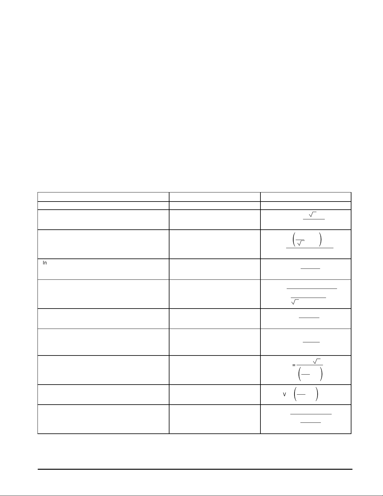
T able 1. Design Equations
Notes Calculation Formula
Calculate the maximum required output power. Required Converter Output Power PO = VO I
Calculated at the minimum required ac line for
regulation. Let the efficiency n = 0.95.
Let the switching cycle t = 20 µs.
In theory the on–time ton is constant. In practice t
tends to increase at the ac line zero crossings due to
the charge on capacitor C6.
The off–time t
approaches zero at the ac line zero crossings.
Theta (θ) represents the angle of
the ac line voltage.
The minimum switching frequency occurs at peak ac
line and increases as t
Set the current sense threshold VCS to 1.0 V for
universal input (85 Vac to 265 Vac) operation and
to 0.5 V for fixed input (92 Vac to 138 Vac, or
184 to 276 Vac) operation.
Set the multiplier input voltage VM to 3.0 V at high
line. Empirically adjust VM for the lowest distortion
over the ac line range while guaranteeing startup at
minimum line.
The IIB R1 error term can be minimized with a divider
current in excess of 100 µA.
The bandwidth is typically set to 20 Hz for minimum
output ripple over the ac line haversine.
The following converter characteristics must be chosen:
– Desired output voltage – AC RMS line voltage
V
O
I
– Desired output current – AC RMS low line voltage
O
is greatest at peak ac line and
off
decreases.
off
Vac
on
Vac
(LL)
Peak Inductor Current
Inductance
Switch On–Time
Switch Off–Time
Switching Frequency
Peak Switch Current
Multiplier Input Voltage
Converter Output Voltage
Error Amplifier Bandwidth
L =
t
=
off
VO = V
BW =
I
=
L(pk)
V
ǒǓ
2t
VO Vac
ton =
2 Vac
f =
R9 =
VM =
R
ref
R
2 π C
22 P
ηVac
O
– Vac Vac
2
(LL) IL(pk)
2 PO L
η Vac
t
on
V
O
Sin θ
1
ton + t
off
V
CS
I
L(pk)
Vac
R
7
+ 1
R
3
2
+ 1
1
1
R1 R
R1 + R
O
(LL)
2
2
Ǔǒ
2
2
O
– 1
Ǔǒ
– IIB R
1
2
2
MOTOROLA ANALOG IC DEVICE DATA
7
Page 8

92 to
138 Vac
RFI
Filter
MC34261 MC33261
Figure 15. 80 W Power Factor Controller
C
1
6
D
D
2
4
+
Zero Current
D
D
1
3
Detector
2.5V
1.2V
+
+
1.6V
UVLO
36V
6.7V
Reference
16V
Drive
Output
Delay
Timer
R
RS
Latch
+
10V
10
10
100k
R
8
8
5
7
1N4934
+
100
C
5
22k
R
10
R
D
6
T
5
MUR130
MTP
8N50E
Q
6
1
V
D
O
5
+
100
C
4
230V/0.35A
0.01
C
2
2.2M
R
7
7.5k
R
330
Current Sense
Comparator
0.5mA
Error Amp
+
4
V
ref
1.0nF
C
3
R
4
Multiplier
3
3
6
2
1
0.1
R
1.0M
R
2
9
11k
R
1
0.68
C
1
Power Factor Controller Test Data
AC Line Input DC Output
Current Harmonic Distortion (%)
V
rms
90 85.6 –0.998 2.4 0.11 0.52 1.3 0.67 10.0 230 0.350 80.5 94.0
100 85.1 –0.997 5.0 0.13 1.7 2.4 1.4 10.1 230 0.350 80.5 94.6
110 84.8 –0.997 5.3 0.12 2.5 2.6 1.5 10.2 230 0.350 80.5 94.9
120 84.5 –0.997 5.8 0.12 3.2 2.7 1.4 10.2 230 0.350 80.5 95.3
130 84.2 –0.996 6.6 0.12 4.0 2.8 1.5 10.2 230 0.350 80.5 95.6
138 84.1 –0.995 7.2 0.13 4.5 3.0 1.6 10.2 230 0.350 80.5 95.7
This data was taken with the test set–up shown in Figure 17.
Heatsink
P
T
= Coilcraft N2881–A
= AAVID Engineering Inc. 5903B, or 5930B
PF THD 2357V
in
Primary: 62 turns of # 22 AWG
Secondary: 5 turns of # 22 AWG
Core: Coilcraft PT2510, EE 25
Gap: 0.072″ total for a primary inductance of 320 µH
O(pp)
V
I
O
O
P
O
n(%)
8
MOTOROLA ANALOG IC DEVICE DATA
Page 9

85 to 265
Vac
RFI
Filter
MC34261 MC33261
Figure 16. 175 W Universal Input Power Factor Controller
C
1
6
D
D
2
4
+
Zero Current
D
D
1
3
Detector
2.5V
1.2V
+
+
1.6V
UVLO
36V
6.7V
Reference
Timer R
Delay
16V
Drive
Output
RS
Latch
+
10V
10
10
100k
R
8
8
5
7
1N4934
+
100
C
22k
R
5
10
R
D
6
T
5
MUR460
MTW
14N50E
Q
6
1
V
D
O
5
+
180
C
4
400V/0.44A
0.01
C
2
1.3M
R
7
12k
R
3
Current Sense
Comparator
3
330
1.0nF
C
3
R
4
0.5mA
Error Amp
+
4
V
ref
Multiplier
1
6
2
0.1
R
1.6M
R
9
10k
R
1
0.68
C
1
Power Factor Controller Test Data
AC Line Input DC Output
Current Harmonic Distortion (%)
V
rms
90 187.5 –0.998 2.0 0.10 0.98 0.90 0.78 8.0 400.7 0.436 174.7 93.2
120 184.6 –0.997 1.8 0.09 1.3 1.3 0.93 8.0 400.7 0.436 174.7 94.6
138 183.6 –0.997 2.3 0.05 1.6 1.5 1.0 8.0 400.7 0.436 174.7 95.2
180 181.0 –0.995 4.3 0.16 2.5 2.0 1.2 8.0 400.6 0.436 174.7 95.6
240 179.3 –0.993 6.0 0.08 3.7 2.7 1.4 8.0 400.6 0.436 174.7 97.4
268 178.6 –0.992 6.7 0.16 2.8 3.7 1.7 8.0 400.6 0.436 174.7 97.8
This data was taken with the test set–up shown in Figure 17.
Heatsink
P
T
= Coilcraft N2880–A
= AAVID Engineering Inc. 5903B
PF THD 2357V
in
Primary: 78 turns of # 16 AWG
Secondary: 6 turns of # 18 AWG
Core: Coilcraft PT4215, EE 42–15
Gap: 0.104″ total for a primary inductance of 870 µH
O(pp)
V
I
O
O
P
O
2
n(%)
MOTOROLA ANALOG IC DEVICE DATA
9
Page 10
MC34261 MC33261
Figure 17. Power Factor Test Set–Up
2X Step–Up
Isolation
Line
115 Vac
Input
Neutral
Earth
Transformer
Autoformer
AC POWER ANALYZER
PM 1000
OI
HIHI
ArmsVrmsPFVAW
53210
HARMFREQ
AinstAcfVcf
1397
11
LO
LO
VA
Voltech
0.1
An RFI filter is required for best performance when connecting the preconverter directly to the AC line. Commercially available two stage filters
such as the Delta Electronics 03DPCG5 work excellent. The simple single stage test filter shown above can easily be constructed with a common
mode transformer . T ransformer (T) is a Coilcraft CMT3–28–2 with 28 mH minimum inductance and a 2.0 A maximum current rating.
RFI Filter
T
0.005
1.0
0.005
0 to 270 Vac
Output Power Factor
Controller Circuit
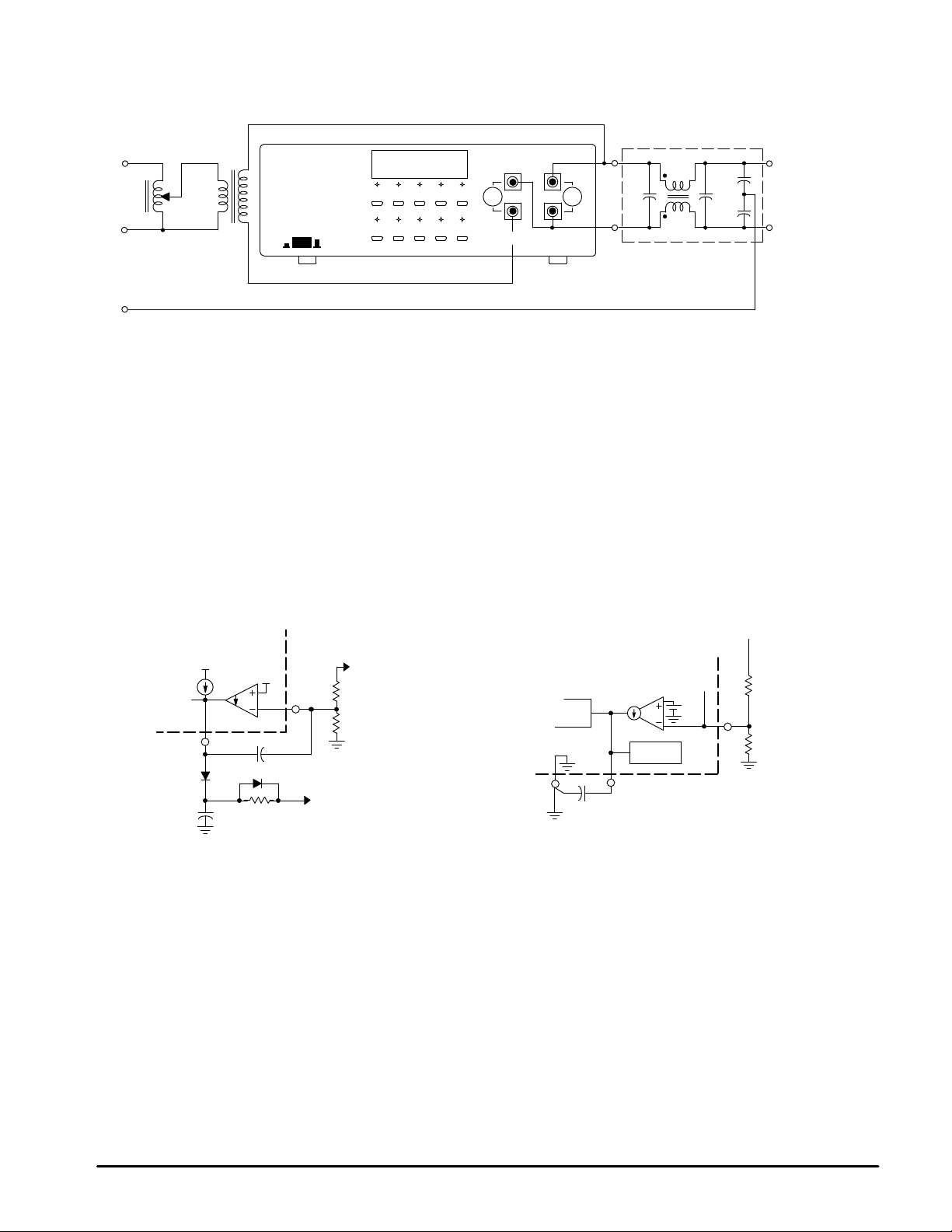
Figure 18. Soft–Start Circuit
+
0.5 mA
1
2
+
C
1.0M
t
Soft–Start
≈
9000C in µF
Startup overshoot can be eliminated with the
addition of a Soft–Start circuit.
To V
To V
CC
Figure 19. Error Amp Compensation
O
Error Amp
10µA
6
2
C
1
+
R
2
1
R
1
10
MOTOROLA ANALOG IC DEVICE DATA
Page 11

MC34261 MC33261
Figure 20. Printed Circuit Board and Component Layout
(Circuits of Figures 15 and 16)
MOTOROLA ANALOG IC DEVICE DATA
11
Page 12

NOTE 2
–T–
SEATING
PLANE
H
58
–B–
14
F
–A–
C
N
D
K
G
0.13 (0.005) B
M
T
–A–
58
4X P
–B–
14
MC34261 MC33261
OUTLINE DIMENSIONS
P SUFFIX
PLASTIC PACKAGE
CASE 626–05
ISSUE K
L
J
M
M
A
M
PLASTIC PACKAGE
CASE 751–05
0.25 (0.010)MB
D SUFFIX
(SO–8)
ISSUE N
M
NOTES:
1. DIMENSION L TO CENTER OF LEAD WHEN
FORMED PARALLEL.
2. PACKAGE CONTOUR OPTIONAL (ROUND OR
SQUARE CORNERS).
3. DIMENSIONING AND TOLERANCING PER ANSI
Y14.5M, 1982.
DIM MIN MAX MIN MAX
A 9.40 10.16 0.370 0.400
B 6.10 6.60 0.240 0.260
C 3.94 4.45 0.155 0.175
D 0.38 0.51 0.015 0.020
F 1.02 1.78 0.040 0.070
G 2.54 BSC 0.100 BSC
H 0.76 1.27 0.030 0.050
J 0.20 0.30 0.008 0.012
K 2.92 3.43 0.115 0.135
L 7.62 BSC 0.300 BSC
M ––– 10 ––– 10
N 0.76 1.01 0.030 0.040
NOTES:
1. DIMENSIONING AND TOLERANCING PER
ANSI Y14.5M, 1982.
2. CONTROLLING DIMENSION: MILLIMETER.
3. DIMENSIONS A AND B DO NOT INCLUDE
MOLD PROTRUSION.
4. MAXIMUM MOLD PROTRUSION 0.15 (0.006)
PER SIDE.
5. DIMENSION D DOES NOT INCLUDE DAMBAR
PROTRUSION. ALLOWABLE DAMBAR
PROTRUSION SHALL BE 0.127 (0.005) TOTAL
IN EXCESS OF THE D DIMENSION AT
MAXIMUM MATERIAL CONDITION.
INCHESMILLIMETERS
__
G
R
X 45
C
–T–
8X D
Motorola reserves the right to make changes without further notice to any products herein. Motorola makes no warranty , representation or guarantee regarding
the suitability of its products for any particular purpose, nor does Motorola assume any liability arising out of the application or use of any product or circuit, and
specifically disclaims any and all liability, including without limitation consequential or incidental damages. “T ypical” parameters which may be provided in Motorola
data sheets and/or specifications can and do vary in different applications and actual performance may vary over time. All operating parameters, including “Typicals”
must be validated for each customer application by customer’s technical experts. Motorola does not convey any license under its patent rights nor the rights of
others. Motorola products are not designed, intended, or authorized for use as components in systems intended for surgical implant into the body, or other
applications intended to support or sustain life, or for any other application in which the failure of the Motorola product could create a situation where personal injury
or death may occur. Should Buyer purchase or use Motorola products for any such unintended or unauthorized application, Buyer shall indemnify and hold Motorola
and its officers, employees, subsidiaries, affiliates, and distributors harmless against all claims, costs, damages, and expenses, and reasonable attorney fees
arising out of, directly or indirectly, any claim of personal injury or death associated with such unintended or unauthorized use, even if such claim alleges that
Motorola was negligent regarding the design or manufacture of the part. Motorola and are registered trademarks of Motorola, Inc. Motorola, Inc. is an Equal
Opportunity/Affirmative Action Employer.
SEATING
PLANE
K
SS
A0.25 (0.010)MTB
_
M
_
J
F
DIM MIN MAX MIN MAX
A 4.80 5.00 0.189 0.196
B 3.80 4.00 0.150 0.157
C 1.35 1.75 0.054 0.068
D 0.35 0.49 0.014 0.019
F 0.40 1.25 0.016 0.049
G 1.27 BSC 0.050 BSC
J 0.18 0.25 0.007 0.009
K 0.10 0.25 0.004 0.009
M 0 7 0 7
P 5.80 6.20 0.229 0.244
R 0.25 0.50 0.010 0.019
INCHESMILLIMETERS
____
Mfax is a trademark of Motorola, Inc.
How to reach us:
USA/EUROPE/Locations Not Listed: Motorola Literature Distribution; JAP AN: Nippon Motorola Ltd.: SPD, Strategic Planning Office, 4–32–1,
P.O. Box 5405, Denver, Colorado 80217. 303–675–2140 or 1–800–441–2447 Nishi–Gotanda, Shinagawa–ku, Tokyo 141, Japan. 81–3–5487–8488
Mfax: RMFAX0@email.sps.mot.com – TOUCHTONE 602–244–6609 ASIA/P ACIFIC: Motorola Semiconductors H.K. Ltd.; 8B Tai Ping Industrial Park,
– US & Canada ONLY 1–800–774–1848 51 Ting Kok Road, T ai Po, N.T., Hong Kong. 852–26629298
INTERNET: http://motorola.com/sps
12
◊
MOTOROLA ANALOG IC DEVICE DATA
MC34261/D
 Loading...