

Page 1
T
A
= 0° to +70°C
Device
Operating
Temperature Range
Package
SEMICONDUCTOR
TECHNICAL DATA
PROGRAMMABLE
TELEPHONE LINE
INTERFACE CIRCUIT WITH
LOUDSPEAKER AMPLIFIER
ORDERING INFORMATION
MC34216ADW SO–28L
DW, DWF SUFFIX
PLASTIC PACKAGE
CASE 751F
28
1
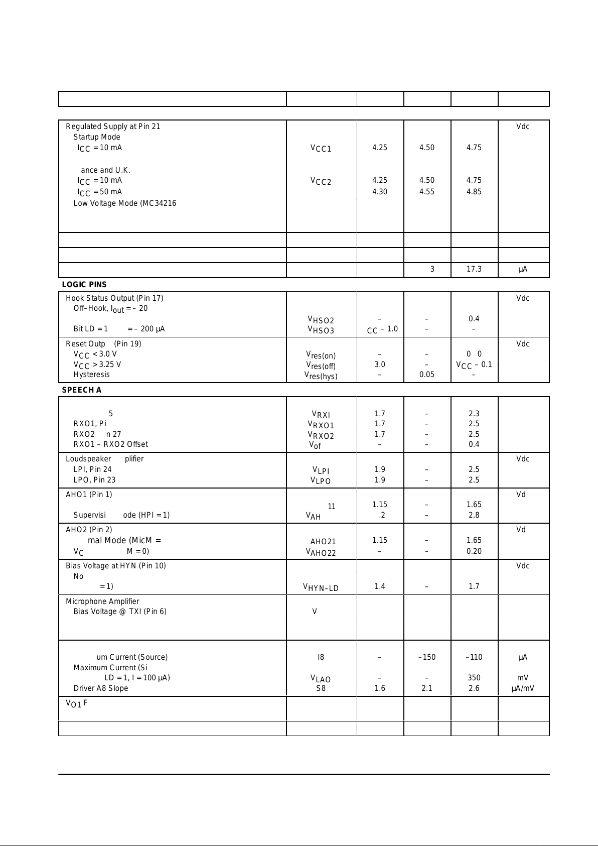
PIN CONNECTIONS
Order this document by MC34216A/D
1 28
27
26
25
24
23
22
21
2
3
4
5
6
7
8
AHO1
AHO2
MTF
MTC
Mic
AGC
RXO1
LPI
Gnd
V
CC
20
9
LAO
LAI
I
ref
1910
HYN
R
S
LPO
RXI
RXO2
AGnd
TXI
(Top View)
18
11
NDC
Clk
17
12
CM D/HS
16
13
IMP
Osc
15
14
SAO SAI
MC34216ADWF SO–28L
1
MOTOROLA ANALOG IC DEVICE DATA
!
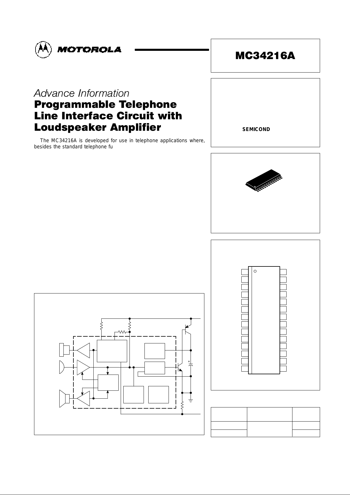
The MC34216A is developed for use in telephone applications where,
besides the standard telephone functions, the group listening–in feature is
also required. In cooperation with a microcontroller, the circuit performs all
basic telephone functions including DTMF generation and pulse–dialing.
The listening–in part includes a loudspeaker amplifier, an anti–howling
circuit and a strong supply. In combination with the TCA3385, the ringing is
performed via the loudspeaker.
• Programmable DC Mask, for France, U.K., and Voltage Regulated
Countries
• DC Mask for France and U.K. (MC34216ADWF)
• Programmable Volume for Listening–In and Ringing
• Small Amount of External Components
• On–Chip DTMF and Ring Signal Generator
• Efficient Supply Point for Loudspeaker Amplifier and Peripherals
• Programmable Modes for Speakerphone, Answering Machine, Fax and
Modem Applications
• Pilot and Idle Tones Provide Extra Phone Features
Simplified Block Diagram
This device contains 6,507 active transistors.
Line
Driver
Anti–
Howling
Mic
Supply
Stabilizer
DC Mask
Generation AC
Termination 2–4
Wire Conversion
DC and AC
Termination
Handset
Earpiece
Handset
MIcrophone
Line –
Line +
LSP
Base
Loudspeaker
Micro-
controller
Interface
DTMF and
Ring
Generator
Ear
This document contains information on a new product. Specifications and information
herein are subject to change without notice.
Motorola, Inc. 1996
Page 2
MC34216A
2
MOTOROLA ANALOG IC DEVICE DATA
FEATURES
Line Driver and Supply
• DC and AC Termination of the Line
• Programmable DC Mask: France, U.K., Startup, Low Voltage (MC34216ADW)
• Programmable DC Mask: France, U.K., Startup (MC34216ADWF)
• Current Protection
• Adjustable Set Impedance for Resistive and Complex Termination
• Efficient Supply Point for Loudspeaker Amplifier and Peripherals
Handset Operation
• Transmit and Receive Amplifiers
• Adjustable Sidetone Network
• Line Length AGC
• Microphone and Earpiece Mute
• Earpiece Gain Increase Switch
• Microphone Squelch Function
• Transmit Amplifier Soft Clipping
Dialing and Ringing
• Generates DTMF, Pilot Tones and Ring Signal
• Interrupter Driver for Pulse–Dialing
• Low Current While Pulse–Dialing
• Optimized for Ringing via Loudspeaker
• Programmable Ring Melodies
• Uses Inexpensive 500 kHz Resonator
Loudspeaking Facility
• Integrated Loudspeaker Amplifier
• Peak–to–Peak Limiter Prevents Distortion
• Programmable Volume
• Anti–Howling Circuitry for Group Listening–In
• Interfacing for Handsfree Conversation
Application Areas
• Corded Telephony with Group Listening–In
• Cordless Telephony Base Station with Group Listening–In
• Telephones with Answering Machines
• Fax, Intercom, Modem
MAXIMUM RATINGS
Rating Symbol Min Max Unit
Maximum Junction Temperature T
J
– +150 °C
Storage Temperature Range T
stg
– 65 +150 °C
NOTES: 1. Devices should not be operated at or outside these values. The “Recommended
Operating Limits” provide for actual device operation.
2.ESD data available upon request.
RECOMMENDED OPERATING CONDITIONS
Characteristic Symbol Min Typ Max Unit
Oscillator Frequency @ Pin 16
f
osc
495
500
505
ÁÁÁ
ÁÁÁ
ÁÁÁ
kHz
Operating Temperature Range
T
A
0
–
+70
ÁÁÁ
ÁÁÁ
ÁÁÁ
°C
Page 3
MC34216A
3
MOTOROLA ANALOG IC DEVICE DATA
DC ELECTRICAL CHARACTERISTICS (T
A
= 25°C)
Characteristic
Symbol Min Typ Max Unit
VOLTAGE REGULATOR
Regulated Supply at Pin 21
Vdc
Startup Mode
ICC = 10 mA V
CC1
4.25 4.50 4.75
ICC = 100 mA 4.40 4.65 4.90
France and U.K.
ICC = 10 mA V
CC2
4.25 4.50 4.75
ICC = 50 mA 4.30 4.55 4.85
Low Voltage Mode (MC34216ADW Only)
ICC = 10 mA V
CC3
3.60 3.90 4.20
ICC = 100 mA 3.75 4.05 4.35
Current Consumption at Pin 21, Bit LD = Hi
ICC LD
–
1.2
–
mA
Regulated Supply in Protection Mode, ICC = 30 mA
V
CC5
4.30
–
4.80
Vdc
Reference Current @ Pin 20
I
ref
15.3
16.3
17.3
µA
LOGIC PINS
Hook Status Output (Pin 17)
Vdc
Off–Hook, I
out
= – 200 µA V
HSO1
VCC – 1.0 – –
On–Hook, I
out
= 200 µA V
HSO2
– – 0.4
Bit LD = 1, I
out
= – 200 µA V
HSO3
VCC – 1.0 – –
Reset Output (Pin 19)
Vdc
VCC < 3.0 V V
res(on)
– – 0.40
VCC > 3.25 V V
res(off)
3.0 – VCC – 0.1
Hysteresis V
res(hys)
– 0.05 –
SPEECH AMPLIFIERS
Earpiece Amplifier DC Bias
Vdc
RXI, Pin 25 V
RXI
1.7 – 2.3
RXO1, Pin 26 V
RXO1
1.7 – 2.5
RXO2, Pin 27 V
RXO2
1.7 – 2.5
RXO1 – RXO2 Offset V
offset
– – 0.4
Loudspeaker Amplifier
Vdc
LPI, Pin 24 V
LPI
1.9 – 2.5
LPO, Pin 23 V
LPO
1.9 – 2.5
AHO1 (Pin 1)
Vdc
Normal Mode (HPI = 0) V
AHO11
1.15 – 1.65
Supervision Mode (HPI = 1) V
AHO12
2.2 – 2.8
AHO2 (Pin 2)
Vdc
Normal Mode (MicM = 1)
V
AHO21
1.15 – 1.65
VCC = 3.5 (MicM = 0) V
AHO22
– – 0.20
Bias Voltage at HYN (Pin 10)
Vdc
Normal Mode V
HYN
2.4 – 2.7
Bit (LD = 1) V
HYN–LD
1.4 – 1.7
Microphone Amplifier
Bias Voltage @ TXI (Pin 6) V
TXI
1.7 – 2.0 Vdc
Voltage at MIC @ 1.0 mA ( MicP = 1) V
Mic
– – 0.35
Leakage @ MIC @ 4.5 V (MicP = 0) I
leak
– – 5.5 µA
LAO (Pin 8)
Maximum Current (Source) I8 – –150 –110 µA
Maximum Current (Sink) I8 110 150 –
Voltage (LD = 1, I = 100 µA) V
LAO
– – 350 mV
Driver A8 Slope S8 1.6 2.1 2.6 µA/mV
VO1 Follower (I2 = 0 µA)
V
O1
1.1
1.18
1.3
V
VO1 – V
O2
∆V
O
40 80 120 mV
Voltage at IMP (Pin 13)
V
IMP
2.2
–
2.5
Vdc
Page 4
MC34216A
4
MOTOROLA ANALOG IC DEVICE DATA
DC ELECTRICAL CHARACTERISTICS
(continued) (TA = 25°C)
Characteristic UnitMaxTypMinSymbol
DC MASK CHARACTERISTICS
Startup Mode
Internal Slope ri 300 380 460 mV/µA
Voltage on SAI (I2C = 5.9 µA) V
C
800 – – mV
Voltage on SAI (I2D = 7.1 µA) V
D
– – 1.5 V
Delta Offset Voltage on SAI (I2E = 38 µA) VE – V
D
– – 100 mV
French
Internal Slope ri 76 103 130 mV/µA
Voltage on SAI (I2C = 5.9 µA) V
C
280 – – mV
Voltage on SAI (I2D = 7.1 µA) V
D
– – 460
Delta Offset Voltage on SAI (I2E = 38 µA) VE – V
D
– – 30
U.K.
Internal Slope ri 120 165 210 mV/µA
Voltage on SAI (I2C = 5.9 µA) V
C
420 – – mV
Voltage on SAI (I2D = 7.1 µA) V
D
– – 675
Delta Offset Voltage on SAI (I2E = 38 µA) VE – V
D
– – 40
Low Voltage Mode (MC34216ADW Only)
Internal Slope ri 95 129 165 mV/µA
Voltage on SAI (I2C = 15 µA) V
C
900 – – mV
Voltage on SAI (I2D = 17 µA) V
D
– – 1.5 Vdc
Delta Offset Voltage on SAI (I2E = 20 µA) VE – V
D
– – 100 mV
Overvoltage Protection Threshold (V
LAI
– V
SAO
)
V
clamp1
485
550
615
mV
I
prot
= 60 µA, ICC = 70 mA
Protection Voltage Level (V
LAI
– V
SAO
)
V
clamp2
370
410
450
mV
I
prot
= 60 µA
AC ELECTRICAL CHARACTERISTICS (T
A
= 25°C)
Characteristic
Symbol Min Typ Max Unit
TRANSMIT MODE
French and U.K.
dB
Maximum Transmit Gain (I2 = 5.6 µA) K
µ0
13.5 14.5 15.5
Line Length Regulation (I2 = 27.5 µA) ∆K
µ
5.0 6.0 7.0
Gain in Protection Mode (I2 = 29.5 µA) K
µp
13.5 14.5 15.5
Low Voltage Mode (MC34216ADW Only)
dB
Maximum Transmit Gain (I2 = 3.5 µA) K
µ0
13.5 14.5 15.5
Line Length Regulation (I2 = 7.7 µA) ∆K
µ
4.7 6.0 7.3
Gain in Protection Mode (I2 = 7.7 µA) K
µp
13.5 14.5 15.5
Gain Reduction when Microphone is Muted
∆K
mute
60
–
–
dB
RECEIVE MODE
French
Maximum Internal Transconductance (I2 = 5.6 µA) G
e0
203 230 258 µA/V
Line Length Regulation (I2 = 26 µA) ∆G
e
5.0 6.0 7.0 dB
Protection Mode (I2 = 26 µA) G
ep
203 230 258 µA/V
U.K.
Maximum Internal Transconductance (I2 = 5.6 µA) G
e0
203 230 258 µA/V
Line Length Regulation (I2 = 26 µA) ∆G
e
5.0 6.0 7.0 dB
Protection Mode (I2 = 26 µA) G
ep
203 230 258 µA/V
Low Voltage Mode (MC34216ADW Only)
Maximum Internal Transconductance (I2 = 3.5 µA) G
e0
183 210 241 µA/V
Line Length Regulation (I2 = 7.9 µA) ∆G
e
4.7 6.0 7.3 dB
Protection Mode (I2 = 7.9 µA) G
ep
183 210 241 µA/V
Earpiece Gain Reduction when Muted
∆Ge
mute
60
–
–
dB
Earpiece Gain Variation (EA Bit Changed to 1)
∆G
e1
4.6
5.6
6.6
dB
Page 5
MC34216A
5
MOTOROLA ANALOG IC DEVICE DATA
AC ELECTRICAL CHARACTERISTICS (continued) (T
A
= 25°C)
Characteristic UnitMaxTypMinSymbol
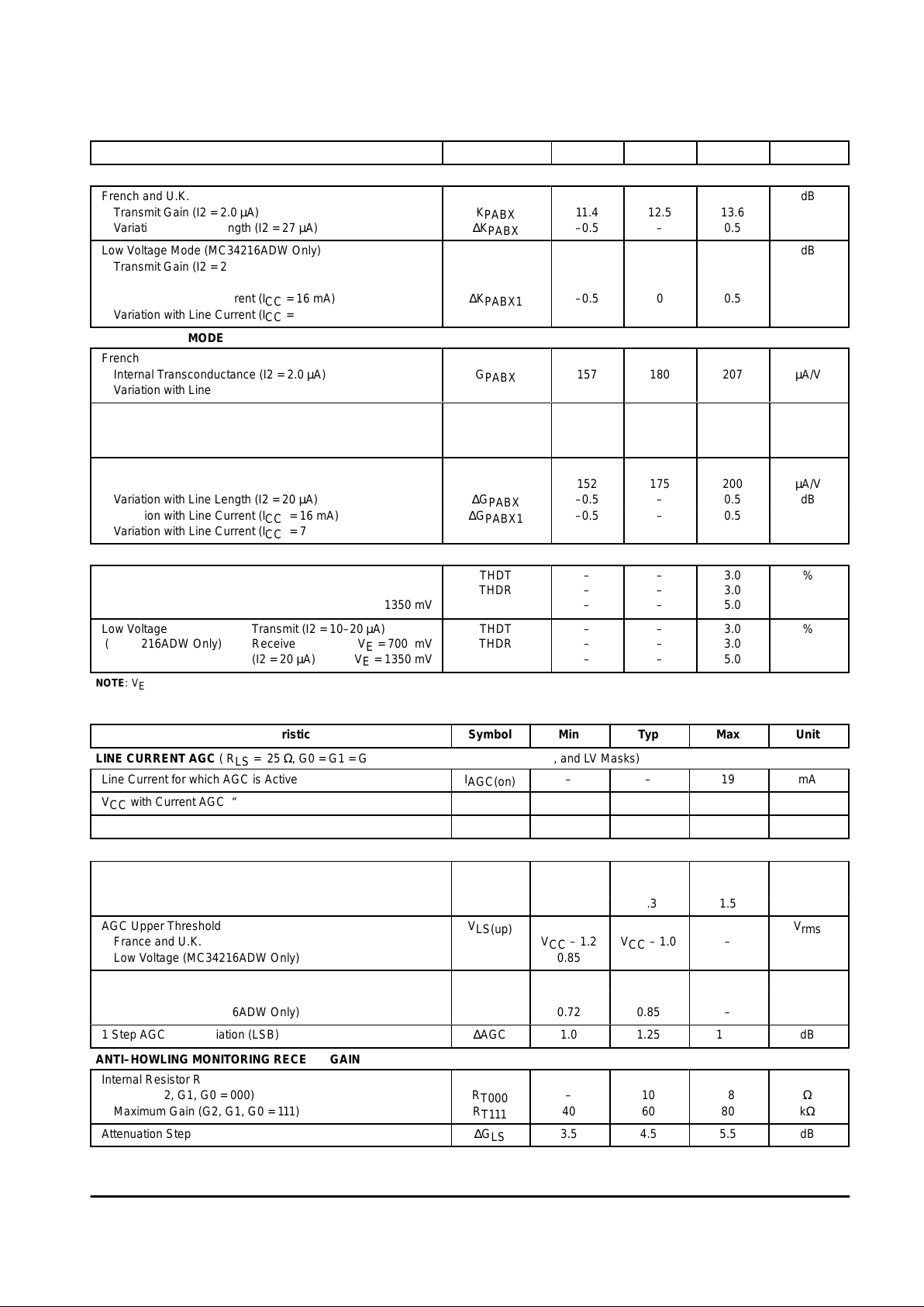
TRANSMIT PABX MODE
French and U.K.
dB
Transmit Gain (I2 = 2.0 µA) K
PABX
11.4 12.5 13.6
Variation with Line Length (I2 = 27 µA) ∆K
PABX
–0.5 – 0.5
Low Voltage Mode (MC34216ADW Only)
dB
Transmit Gain (I2 = 2.0 µA) K
PABX
11.5 12.5 13.6
Variation with Line Length (I2 = 20 µA) ∆K
PABX
–0.5 – 0.5
Variation with Line Current (ICC = 16 mA) ∆K
PABX1
–0.5 0 0.5
Variation with Line Current (ICC = 7.0 mA) ∆K
PABX2
–2.0 0 2.0
RECEIVE PABX MODE
French
Internal Transconductance (I2 = 2.0 µA) G
PABX
157 180 207 µA/V
Variation with Line Length (I2 = 27 µA) ∆G
PABX
–0.5 – 0.5 dB
U.K.
Internal Transconductance (I2 = 2.0 µA) G
PABX
157 180 207 µA/V
Variation with Line Length (I2 = 27 µA) ∆G
PABX
–0.5 – 0.5 dB
Low Voltage Mode (MC34216ADW Only)
Internal Transconductance (I2 = 2.0 µA) G
PABX
152 175 200 µA/V
Variation with Line Length (I2 = 20 µA) ∆G
PABX
–0.5 – 0.5 dB
Variation with Line Current (ICC = 16 mA) ∆G
PABX1
–0.5 – 0.5
Variation with Line Current (ICC = 7.0 mA) ∆G
PABX2
–2.0 – 2.0
DISTORTION
French and U.K. Transmit (I2 = 10–30 µA)
French Receive VE = 700 mV
(I2 = 10 µA) VE = 1350 mV
THDT
THDR
–
–
–
–
–
–
3.0
3.0
5.0
%
Low Voltage Transmit (I2 = 10–20 µA)
(MC34216ADW Only) Receive VE = 700 mV
(I2 = 20 µA) VE = 1350 mV
THDT
THDR
–
–
–
–
–
–
3.0
3.0
5.0
%
NOTE: VE is the differential earpiece voltage across Pins 26 and 27.
OTHER ELECTRICAL CHARACTERISTICS (T
A
= 25°C)
Characteristic
Symbol Min Typ Max Unit
LINE CURRENT AGC ( RLS = 25 Ω, G0 = G1 = G2 = 1, VLS = 2.0 Vpp, French, U.K., and LV Masks)
Line Current for which AGC is Active
I
AGC(on)
–
–
19
mA
VCC with Current AGC “On” (ICC = 13 mA)
VCC
AGCVCC
– 5.0%
V
CC
–
Vdc
Line Current for which AGC is Inactive
I
AGC(off)
21
–
–
mA
PEAK–TO–PEAK AGC (RLS = 25 Ω, C25 = 220 nF, G0 = G1 = G2 = 1, ICC = 40 mA)
DC Level at Pin 28
Vdc
AGC “Off” V
AGC(off)
1.6 1.7 1.8
AGC “On” V
AGC(on)
1.2 1.3 1.5
AGC Upper Threshold
V
LS(up)
V
rms
France and U.K. VCC – 1.2 VCC – 1.0 –
Low Voltage (MC34216ADW Only) 0.85 1.0 –
AGC Lower Threshold
V
LS(low)
V
rms
France and U.K. VCC – 1.9 VCC – 1.6 –
Low Voltage (MC34216ADW Only) 0.72 0.85 –
1 Step AGC Gain Variation (LSB)
∆AGC
1.0
1.25
1.50
dB
ANTI–HOWLING MONITORING RECEIVE GAIN
Internal Resistor R
T
Muted (G2, G1, G0 = 000) R
T000
– 10 18 Ω
Maximum Gain (G2, G1, G0 = 111) R
T111
40 60 80 kΩ
Attenuation Step
∆G
LS
3.5
4.5
5.5
dB
Page 6
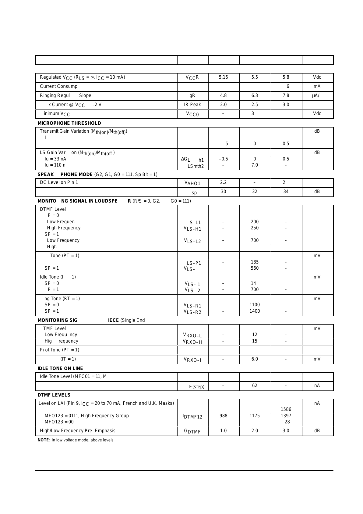
MC34216A
6
MOTOROLA ANALOG IC DEVICE DATA
OTHER ELECTRICAL CHARACTERISTICS
(continued) (TA = 25°C)
Characteristic UnitMaxTypMinSymbol
RINGING MODE REGULATION
Regulated VCC (RLS = ∞, ICC = 10 mA)
VCCR
5.15
5.5
5.8
Vdc
Current Consumption @ VCC = 3.4 V, RLS = ∞
IcR
–
2.0
2.6
mA
Ringing Regulator Slope
gR
4.8
6.3
7.8
µA/V
Peak Current @ VCC = 4.2 V
IR Peak
2.0
2.5
3.0
µA
Minimum V
CC
V
CC0
–
3.8
–
Vdc
MICROPHONE THRESHOLD
Transmit Gain Variation (M
th(on)/Mth(off)
)
dB
Iu = 33 nA ∆K
µmth1
– 7.0 –
Iu = 110 nA ∆K
µmth2
–0.5 0 0.5
LS Gain Variation (M
th(on)/Mth(off)
)
dB
Iu = 33 nA ∆G
LSmth1
–0.5 0 0.5
Iu = 110 nA ∆G
LSmth2
– 7.0 –
SPEAKERPHONE MODE (G2, G1, G0 = 111, Sp Bit = 1)
DC Level on Pin 1
V
AHO1
2.2
–
2.8
Vdc
Speakerphone Gain
G
sp
30
32
34
dB
MONITORING SIGNAL IN LOUDSPEAKER (R/S = 0, G2, G1, G0 = 111)
DTMF Level
mV
SP = 0
Low Frequency V
LS–L1
– 200 –
High Frequency V
LS–H1
– 250 –
SP = 1
Low Frequency V
LS–L2
– 700 –
High Frequency V
LS–H2
– 900 –
Pilot Tone (PT = 1)
mV
SP = 0 V
LS–P1
– 185 –
SP = 1 V
LS–P2
– 560 –
Idle Tone (IT = 1)
mV
SP = 0 V
LS–I1
– 145 –
SP = 1 V
LS–I2
– 700 –
Ring Tone (RT = 1)
mV
SP = 0 V
LS–R1
– 1100 –
SP = 1 V
LS–R2
– 1400 –
MONITORING SIGNAL IN EARPIECE (Single Ended)
DTMF Level
mV
Low Frequency V
RXO–L
– 12 –
High Frequency V
RXO–H
– 15 –
Pilot Tone (PT = 1)
V
RXO–P
–
8.0
–
mV
Idle Tone (IT = 1)
V
RXO–I
–
6.0
–
mV
IDLE TONE ON LINE
Idle Tone Level (MFC01 = 11, MFO123 = 000)
I
IDLE0
400
550
700
nA
Step Size
I
IDLE(step)
–
62
–
nA
DTMF LEVELS
Level on LAI (Pin 9, ICC = 20 to 70 mA, French and U.K. Masks)
nA
MFO123 = 1111, High Frequency Group I
DTMF15
1124 1336 1586
MFO123 = 0111, High Frequency Group I
DTMF12
988 1175 1397
MFO123 = 0000, Low Frequency Group I
DTMF0
373 444 528
High/Low Frequency Pre–Emphasis
G
DTMF
1.0
2.0
3.0
dB
NOTE: In low voltage mode, above levels must be reduced by 0.5 dB.
Page 7

MC34216A
7
MOTOROLA ANALOG IC DEVICE DATA
DTMF FREQUENCIES
Characteristic Min Typ Max Unit DTMF Std % Error
Low Group Frequencies
689.4
696.4
703.4
Hz
697
–0.09
761.5
769.2
776.9
Hz
770
–0.10
844.7
853.2
861.7
Hz
852
0.14
930.5
939.9
949.3
Hz
941
–0.11
High Group Frequencies
1195.6
1207.7
1219.8
Hz
1209
–0.11
1323.5
1336.9
1350.3
Hz
1336
0.07
1464.5
1479.3
1494.1
Hz
1477
0.16
1617.7
1634
1650.3
Hz
1633
0.06
NOTE: Minimum values based on f
osc
= 495 kHz. Maximum values based on f
osc
= 505 kHz.
TEMPERATURE SPECIFICATIONS (T
A
= 65°C)
Characteristic
Symbol Min Max Unit
DTMF Distortion Level on Pin LAI, Delta Levels
(F = Hi Freq – f = 697 Hz)
DTMFD – –27 dB
V
CC2
in FR Mode @ ICC = 50 mA V
CC2
4.15 5.0 V
V
CCR
@ ICC = 10 mA, RLS = ∞ V
CCR
5.0 6.0 V
VC on Pin SAI in FR Mode V
C
220 460 mV
Ri Slope in FR Mode Ri 65 155 kΩ
RT111 Resistor on LS in FR Mode RT111 35 85 kΩ
Kµ0 in FR Mode K
µ0
13 16 dB
Ge0 in FR Mode G
e0
170 270 µA/V
Reset Off @ VCC = 3.25 V V
resoff
3.0 3.25 V
PIN FUNCTION DESCRIPTION
Pin Symbol Description
1 AHO1 Anti–Howling Timing, Speakerphone Input
2 AHO2 Anti–Howling Timing, Low Voltage Line Driver Disable
3 MTF Microphone Threshold Filtering
4 MTC Microphone Threshold Timing
5 AGnd Small Signal Ground
6 TXI Microphone Amplifier Input
7 Mic Microphone Bias Current Sink
8 LAO Line Driver Amplifier Output
9 LAI Line Driver Amplifier Input
10 HYN Hybrid Network Input
11 NDC Noise Decoupling
12 CM DC Mask Signal Filtering
13 IMP Reference Voltage
14 SAO Line Current Sense Amplifier Output
15 SAI Line Current Sense Amplifier Input
16 Osc Oscillator Input. Connect to 500 kHz Resonator
17 D/HS Data Input, Hookstatus Output
18 Clk Clock Input
19 R
S
Reset Output
20 I
ref
Reference Current
Page 8

MC34216A
8
MOTOROLA ANALOG IC DEVICE DATA
PIN FUNCTION DESCRIPTION (continued)
Pin DescriptionSymbol
21 V
CC
Supply Voltage
22 Gnd Large Signal Ground
23 LPO Loudspeaker Amplifier Output
24 LPI Loudspeaker Amplifier Input
25 RXI Receive Amplifier Input
26 RXO1 Receive Amplifier Output
27 RXO2 Receive Amplifier Output
28 AGC Loudspeaker AGC Timing
CIRCUIT DESCRIPTION
Concept
With the MC34216A, a microcontroller and a switched
mode power supply , a telephone set with listening–in function
and ringing via loudspeaker can be built as shown in
Figure 1.
In off–hook position, the application is in speech mode. The
line current flows through transistor T2 and supplies the
application at the supply point VCC which is stabilized by the
MC34216A. The V
line
, I
line
characteristic is programmed by
the microcontroller and adjusted by the external components
Z0, Z1, Z21 and R1 which are in a regulator loop, acting on
transistor T2. The ac impedance is generated in a similar way.
Handset and loudspeaker can be connected directly to the
MC34216A to perform handset and listening–in operation.
Via the bus, the microcontroller programs the MC34216A to
perform the DTMF/pulse–dialing and supervise the device.
The user keyboard has to be connected to the microcontroller.
In on–hook position, the SMPS supplies the application in
presence of a ringing signal. The microcontroller programs
the MC34216A and a ringing melody can be generated via
the loudspeaker.
The block diagram of the MC34216A (see Figure 2),
shows the basic blocks of the device plus the essential
external components.
R1
MicroMC34216A
T2
Z0
Z1
Z21
A/B
Hookswitch
V
CC
Gnd
SMPS
Loudspeaker
Handset
Figure 1. Telephone Concept with MC34216A
Page 9

MC34216A
9
MOTOROLA ANALOG IC DEVICE DATA
T2
C7
RXO1
Z0
Z21
Z1
T3
C20
R6
R9
C5
R12R20
RXO2
TXI
Mic
AHO1 MTCMTFAHO2
RXI
LAO
Gnd
V
HYN NDC SAO LAI IMP
I
Supply–
Stabilizer
References
DC Mask Generation
AC Termination
2–4 Wire Conversion
Line Length AGC
Protection
C12
Line +
Line –
26
27
25
6
7
1
21
22
8
2 3 4
10 11 14 9 13 20
Anti–Howling
Line
Driver
Ear
Mic
Mute, AGC
MC34216A
C17
AGC
28
ref
CC
Mute, AGC
CM
C16
12
To IMP To SAI
To IMP
Ring–
AGnd
5
RS
19
Clk
18
D/HS
17
Regulator
DTMF/Tone
and Ring
Generator
Micro–
Interface
Clock
Hook–Detect
Osc
16
X1
LPO
R30
LPI
23
24
LSP
C24
Volume
Microphone Threshold
C29C28C27C26
C25
To IMP
C21
R28
To
Micro–
controller
R1
SAI
15
Handset
Earpiece
Handset
Microphone
Speaker
Figure 2. Block Diagram of the MC34216A with Essential Components
DC CHARACTERISTICS AND STARTUP
2
1
3
4
VLC
IVLPILKILP
VLK
ILC
VLP
V
I
0
line
line
Region 1: Startup, Low Line Current, High Slope
Region 2: Mid Range Line Current, Small Slope
Region 3: High Line Current, High Slope
Region 4: Overload Protection
Figure 3. General Form of the
DC Mask of the MC34216A
The MC34216A offers the possibility to adjust the dc
characteristics of all 4 regions via both software and hardware
adjustments. The software adjustments make it possible to
program the 4 different basic masks: France, United Kingdom,
Low Voltage and Startup. The hardware adjustments can be
used for fine–tuning. The adjustment possibilities will be
discussed below with the aid of the block diagram of Figure 4.
In Region 1, the transfer of the amplifier G at the HYN input
equals zero. The voltage difference between SAO and SAI
will equal VO1. The slope RE1 of the V
line
, I
line
characteristic
will equal:
R
E1
+
R1 xǒ1
)
Z0
Z21
Ǔ
In Region 2, the output current of the amplifier G will be
proportional to the input current. As a result, the voltage
between SAO and SAI will increase with the line voltage.
Speech signals on the line are of no influence on this
because they are filtered out via capacitor C16. The slope
RE2 of the V
line
, I
line
characteristic will equal:
R
E2
+
R1 x
ȧ
ȡ
Ȣ
1
)
1
Ri
Z1
)
Z21
Z0
ȧ
ȣ
Ȥ
In Region 3, the output current of the amplifier G is kept
constant. As a result, the slope in Region 3 will equal the
slope of Region 1.
Page 10

MC34216A
10
MOTOROLA ANALOG IC DEVICE DATA
Z21
T3
T2
Z1
C12
RX
Z0
R5
V
C7
2V 1.4 V
V
Line +
HYN
LAI
SAONDC
SAI
LAO
Line –
Gnd
I2
R1
MC34216A
C16
2.4 V
IMP
CM
G
CC
O2
BE
V
O1
+
+
+
+
+
+
≈
+
+
Figure 4. DC Part of the Block Diagram of the MC34216A
The transfer from Region 2 to 3 occurs at the point VLK,
ILK, which is calculated:
VLK+Z1 x I2CD)2VBE)
VCD)
V
O2
ILK
+
Z21
Z0
xǒZ1 x I2CD)2V
BE
Ǔ
)
V
CD
R1
With : I2CD
+
I2C)I2D
2
, and VCD+
VC)
V
D
2
,
and 2VBE[
1.4 V, VO2[
1.1 V
When the French or U.K. mask is selected, this transfer
takes place for line currents of 30 mA to 40 mA depending
on the components settings. With the Startup and Low
Voltage mask, the transfer lies outside the normal operating
range with line currents of 90 mA or more. In most
applications, the transfer from Region 1 to 2 takes place for
line currents below 10 mA.
With proper settings, Region 4 is only entered during an
overload condition. In this mode, the power consumption in
the telephone set is limited. In order to detect an overload
condition, the voltage between the Pins LAI and SAO is
monitored. When the voltage difference is larger than the
threshold V
clamp1
, the protection is made active. The relation
for the line voltage VLP at this point is given as:
VLP
+
Z0
Z21
x V
clamp1
)
VCD)
V
O2
When the protection mode is entered, the line current is
reduced to a lower value ILP of:
ILP
+
V
clamp2
)
ǒ
VO1– V
O2
Ǔ
R1
When the line voltage becomes smaller than VLP, the
overload condition is gone and the MC34216A will leave
Region 4.
The current drawn from the line by the dc part is used to
supply the MC34216A and peripheral circuits. The surplus of
current is sunk away by the voltage stabilizer at Pin V
CC
where a reservoir capacitor is connected. The reference for
the circuit is Pin Gnd.
Startup of the application is ensured by an internal startup
circuit. During the startup, the internal registers of the
MC34216A are reset, and the reset Pin RS goes high. This
signals is meant to indicate to the microcontroller that the
programming of the MC34216A can start.
When the line current flows, the hook status output
Pin D/HS goes high. This serves as the information for the
microcontroller that the set is off–hook. When the line current
is no longer present, the pin goes low again. Because the line
current is monitored, and not the line voltage, an interrupt of
the exchange can be recognized.
Page 11

MC34216A
11
MOTOROLA ANALOG IC DEVICE DATA
AC CHARACTERISTICS
Impedance
In Figure 5, the block diagram of the MC34216A
performing the ac impedance is depicted. As can be seen, it
is partly in common with the dc mask block diagram. The part
generating the dc mask is replaced by a dc voltage source
because for ac, this part has no effect.
Z21
T3
T2
Z0
R5
V
C7
V
LAI
SAO
SAI
LAO
Gnd
R1
MC34216A
CC
O2
V
O1
Line +
Line –
+
+
+
+
Figure 5. AC Stage of the MC34216A
When calculating the ac loop, it can be derived that the set
impedance Zin equals:
Z
in
+
V
line
I
line
+
R1ǒ1
)
Z0
Z21
Ǔ
[
R1 x
Z0
Z21
As can be noticed, the formula for the ac impedance Z
in
equals the formula for the dc slope in Regions 1 and 3.
However, because for the dc slopes the resistive part of Z0
and Z21 are used, the actual values for Zin and the dc slopes
do not have to be equal.
A complex impedance can be made by making either Z0
or Z21 complex. When Z0 is made complex to fit the set
impedance, the transmit characteristics will be complex as
well. The complex impedance is therefore preferably made
via the Z21 network. Because Z21 is in the denominator of
the Zin formula, Z21 will not be a direct copy of the required
impedance, but a derivative of it. Figure 6 shows the derived
network to be used for Z21.
Cb
Ra
Rb
Rv Rv
Rw
Cw
SAO LAI
Gnd
Rv
+
R1 x Z0
2(Ra)Rb – R1
)
Rw
+
R1 x Z0(Ra – R1
)
4Rb(Ra)Rb – R1
)
Cw
+
4Rb
2
x Cb
R1 x Z0
Figure 6. Derived Network for Z21 in Case
of Complex Set Impedance
Transmit
When on Pin LAI a current is injected, via the loop
depicted in Figure 5, a signal is created on the line. In this
way, the microphone signals and DTMF signals from the
internal generator are transmitted. It can be derived that the
signal voltage on the line (V
line
) depends on the signal
current injected in LAI (I
LAI
) according to:
V
line
+
–I
LAI
x
Z0 x Z
line
Zin)
Z
line
With this relation, a simplified replacement circuit can be
made for the transmit amplifier (see Figure 7). Here the
product of I
LAI
and Z0 is replaced by one voltage source.
Z
+
–
line
Z
in
V
line
–I
LAI
*Z0
+
Figure 7. Replacement Diagram for the
Transmit Amplifier
The microphone signal current is derived from the
microphone signal according to the schematic in Figure 8.
Ru
Cmic
Cu
R
MIC
TXI
Microphone
Handset
Ku
Line AGC
Iu
MC34216A
Microphone Threshold
V
CC
R
I
LAI
TXI
Mic
Figure 8. Microphone Amplifier Input Stage
The input stage in Figure 8 consists of a current amplifier
with transfer Ku and impedance R
TXI
= 1.0 kΩ plus an
attenuator which reduces the signal current at high line
currents, the so–called line length regulated gain or line AGC.
This attenuator can be switched on/off via the microcontroller.
The input current Iu within the telephony speech band is
derived from the microphone signal according to:
Iu
+
Vu
R
Mic
)Ru)
R
TXI
[
Vu
Ru
With: Vu = signal of the microphone only loaded with R
Mic
.
The overall gain from microphone to line (ATX) now follows
as:
ATX+
V
line
Vu
+
Ku
Ru
x
Z0 x Z
line
Zin)
Z
line
Practically, the gain can only be varied with Z0, Ru and
R
Mic
.
Page 12

MC34216A
12
MOTOROLA ANALOG IC DEVICE DATA
2.4 V
2V
C17
R20
Z1
R1
RXO2
–1 X
IMP
HYN
RXO1
SAI
Handset
Earpiece
C
Line AGC
V
Line +
Line –
RXI
Gnd
MC34216A
BE
+ V
O1
ref
load
R
load
G
C
ear
e
+
+
+
+
Figure 9. Receive Part of the MC34216A
The noise which is transmitted to the line can be reduced
when the microphone threshold feature is enabled. This is
also called squelch. When there is no microphone signal
present, the transmit gain is reduced by 7.0 dB with respect
to nominal. In between, the gain is varied in steps of 1.0 dB
dependent on the signal level. The detection of the
microphone signal level is done via an integrator which uses
the external capacitors C28 and C29 for timing and filtering.
This feature is also very useful to reduce the howling effect
during listening–in.
The MC34216A offers the possibility to mute the
microphone, also called privacy mode. In this case, the far
end user no longer hears the local user. It is possible to send
during this mode an idle tone to the line to make the far end
user aware of this.
During pulse–dialing, the microphone biasing can be
switched off by programming. Pin Mic will then be made high
impedance, meaning that the microphone dc current no
longer flows into this pin. This reduces the current
consumption of the application during pulse–dialing. It can
also be used to disconnect the handset microphone signal
and enable another transmit signal, for instance from a
handsfree microphone.
Receive
The receive portion of the MC34216A is shown in Figure 9.
The receive signal is picked up by the amplifier at the HYN
input. This is the same amplifier as present in the dc loop of
Figure 4. The signal is first converted to current by the
transconductance amplifier with transfer Ge. The multiplier
placed after performs line length dependent gain or line AGC.
Afterwards, the current is converted back to voltage via the
external feedback network Z
load
. The resulting voltage is
available at output RXO1, and at RXO2 which is the inverted
earpiece output.
From the diagram of Figure 9 the receive gain (ARX) can
be derived as:
With :
A
RX
+
V
RXO
V
line
+
Gex R1 x Z
load
x
ǒ
1
Z
h
)
1
Z
in
Ǔ
Zh+
R1 x Z1
R20
,
also see the sidetone characteristics below.
The earpiece can either be connected as a single–ended
or as a bridge–tied load. The above calculated gain is valid
for the single–ended case. When connecting as a bridge–tied
load, the gain is increased by 6.0 dB.
The MC34216A offers the possibility to increase the
receive gain to the earpiece with an extra 6.0 dB via the
microcontroller on command of the user of the telephone set.
This is useful for people with hearing problems or when the
far end user speaks very softly.
The MC34216A offers the possibility to mute the signal
coming from the line to the earpiece. This is useful during
pulse–dialing or to mute the far end user.
Sidetone
When a transmit signal is transmitted to the line, a part of
the signal is returned to the receive channel due to the nature
of the 2 to 4 wire conversion of the hybrid. During transmit,
the signal on the line will be –I
line
x Z
line
. During receive, the
signal on the line will be I
line
x Zin. When replacing Zin in the
formula for the receive gain, it follows that the signal on the
earpiece output due to a sending signal on the line will be:
V
ear
V
line–transmit
+
Gex R1 x Z
load
x
ǒ
1
Z
h
–
1
Z
line
Ǔ
The sidetone can be minimized by making Zh equal to
Z
line
. A complex sidetone network can therefore be made via
a complex Z1. The coupling capacitor C17 in series with R20
is only meant to block dc.
Line Length AGC
The MC34216A offers the possibility to vary the transmit
and receive gains over line length in order to compensate for
the loss in gain at longer line lengths. In the block diagrams
of the transmit and receive channels the attenuator
performing the line AGC is already drawn. The line AGC can
be switched on/off via the microcontroller. In case the line
AGC is switched off, the transmit and receive gain are
lowered 2.0 dB with respect to the value calculated via the
formulas above.
The line AGC characteristics for both transmit and receive
channels have the general shape depicted in Figure 10.
Page 13

MC34216A
13
MOTOROLA ANALOG IC DEVICE DATA
ILIL
Reduced
Gain
Nominal
Gain
Gain
I
Gain
+
Nominal Gain
1
)
IL – IL
start
IL
range
range
line
start
Figure 10. General Line AGC Characteristics
For small line currents, and thus long lines, the gains are
nominal. When the line current has increased above IL
start
with a current IL
range
, the gain is reduced by 6.0 dB. Due to
the general characteristics of the line AGC curve, the gain will
be decreased further for higher currents.
For France and the U.K., the line AGC will be active in
Region 3 of the dc characteristics. The IL
start
is approximately
equal to the ILK. The range is determined by:
IL
range
+
Z1 x(I2R – I2CD
)
R
E3
For Low Voltage mask, the line AGC is active in Region 2.
Loudspeaking Facility
The MC34216A incorporates a loudspeaking facility which
facilitates group listening–in with incorporated anti–howling
circuitry, handsfree conversation with external duplex
controller and ringing via loudspeaker with external switched
mode power supply.
Loudspeaker Amplifier
The block diagram of the loudspeaker amplifier which is
incorporated in the MC34216A is depicted in Figure 11.
The first part of the loudspeaker amplifier equals the
receive part of the earphone amplifier. It therefore also
includes the anti sidetone circuit and the line current AGC.
The overall gain from line to loudspeaker output LPO is
therefore:
A
LSP
+
ǒ
1
)
R30
R28
Ǔ
x RTx Gex R1 x
ǒ
1
Z
h
)
1
Z
in
Ǔ
The gain of the loudspeaker amplifier can be adjusted by
the external components as indicated in the formula above.
However, the gain is also influenced by line length AGC,
volume control and the signal limiter AGC.
The influence of line length AGC on the loudspeaker
channel is equal to its influence on the receive amplifier of the
earpiece because it is in their common path.
The volume of the loudspeaker is controlled via the
microcontroller. In total, 8 levels can be programmed: 7 levels
with equal steps of 4.5 dB and one level which completely
mutes the loudspeaker amplifier.
The output signal is limited by an AGC circuit when the
peaks of the signal are larger than a certain threshold (peak
AGC) and when the line current available is not sufficient
(current AGC). This prevents distortion of the output signal
and a drop of the supply voltage VCC.
Listening–In
During group listening–in, both the handset and the
loudspeaker are active. Via the acoustic coupling from
loudspeaker to handset microphone, howling can occur
when the handset is held close to the base. In order to reduce
howling, an anti–howling correlator and a microphone
threshold are incorporated in the MC34216A. Both functions
can be switched on/off via the microcontroller.
The anti–howling correlator monitors the microphone and
loudspeaker signal via capacitors C26 through C29. When
both signals show a high correlation, then both contain a
common signal. In practice, this means that howling is
present. In this case, the anti–howling correlator will reduce
the loudspeaker gain in steps of 1.25 dB, until the correlation
is below a certain threshold.
C24
2.4 V
2V
C17
R20
Z1
R1
IMP
HYN
SAI
C23
Line AGC
Line +
Line –
Gnd
MC34216A
BE
+ V
O1
R30
Anti–
Howl
I
VolumeMicrophone
Threshold
LPO
Signal
Limiter
C25 C21
LPI
ACG
R
R28
Loudspeaker
Control
RX
T
+
+
+
Figure 11. Block Diagram of the Loudspeaker Amplifier
Page 14

MC34216A
14
MOTOROLA ANALOG IC DEVICE DATA
The microphone threshold reduces the gain in the acoustic
feedback loop by 7.0 dB. When there is no, or only a small
microphone signal, the gain in the transmit path is reduced by
7.0 dB with respect to nominal. The loudspeaker gain is then
at its nominal value. At a high microphone input current, the
microphone gain is back to its nominal value and the
loudspeaker gain reduced by 7.0 dB. The behavior of the
microphone threshold feature is depicted in Figure 12.
33 n 110 n
A
A
Gain
Iu (Arms)
Nominal
Reduced
TX
LSP
Figure 12. Behavior of the Microphone
Threshold Feature
Handsfree
A speakerphone application for handsfree conversation
can easily be made with the MC34216A by adding one of
the Motorola speakerphone cores to it. The TXI input can be
used to amplify the transmit signal and the earphone output
can be used to monitor the receive signal. The receive
output of the speakerphone core can be connected to
AHO1. When programming the MC34216A in speakerphone
mode, the signal on this pin will be amplified to the
loudspeaker output. In this way, the features and
functionality of the MC34216A are optimally used, like its
powerful supply, loudspeaker amplifier with anti–distortion
circuitry and line current regulation. More details about this
application can be found in the user manual.
Ringing
The MC34216A offers the possibility to generate a ringing
melody via the loudspeaker, which avoids the use of a piezo
buzzer. The power needed to supply the loudspeaker is
transformed out of the ringer signal by a switched mode
power supply TCA3385. The melody is generated by the
MC34216A and programmed via the microcontroller. This
concept is depicted in Figure 13.
As can be seen in Figure 13, the high voltage ring signal is
first transformed into a low voltage supply point with high
current capability. This is needed because, compared to a
piezo resonator, a loudspeaker is low ohmic. In the ringing
mode, the voltage of the supply point is stabilized by the
MC34216A to 5.5 V . The ringing melody can be programmed
via the microcontroller and is generated internally. The output
signal level is regulated via a gain control loop. The loop
couples the value of VCC to the output current of the ringing
melody generator. No ringing melody is made audible when
VCC is below 3.8 V and the maximum volume is reached
when VCC has reached 5.5 V.
To ensure optimum output power under low line current
conditions, the current consumption of the MC34216A in
ringing mode is reduced down to 2.0 mA.
The MC34216A offers the possibility to listen to the ringing
melody while in the speech mode. Although the feeding
conditions are not equal for ringing and speech mode, this
offers the user the possibility to program his own melody and
to adjust the volume.
Hookswitch
R4 C4
Bus
C8
R24
T1
L1
D10
R30
R1
C24
RDO
Gnd
R
LI
Ringer
Supply
Regulator
and Melody
Generator
Micro-
controller
LPI
LPO
Gnd
Off Hook
Application
I
SAI of
MC34216A
TCA3385
MC34216A
CO
DRV
V
C7
CC
V
CC
Phone Line
R
in
Figure 13. Concept of Ringing Via Loudspeaker
Page 15

MC34216A
15
MOTOROLA ANALOG IC DEVICE DATA
Programming Possibilities
The MC34216A can be programmed by a microcontroller
via a 2 wire bus. In this way, it is possible to program the dc
mask, DTMF tones, listening–in mode, loudspeaker volume,
etc.
The bus interface of the microcontroller with the
MC34216A consists of 2 wires: a data wire and a clock wire
connected to Pins D/HS and CLK respectively. Also, the
reset Pin RST of the MC34216A is connected to the
microcontroller. The MC34216A itself has a local oscillator
connected to Pin Osc.
The local oscillator needs a 500 kHz parallel mode
ceramic resonator, with approximately 75 pF capacitance,
connected to ground (for instance, the TOKO
FCRK500A–P35). The local oscillator is the reference for all
the internal timings of the MC34216A.
The 2 wire bus is based on the SCI standard. This
standard includes things such as de–bouncing and bus
monitoring in order to check that the data is sent over
correctly. The full bus specification is depicted in Figure 14.
The data is read in during the falling edge of the clock signal.
The clock has to be active only during the transfer of the data.
After the data is sent, the clock has to be kept low.
The D/HS pin is not only the input for the data but also the
output for the hookswitch information. When there is line
current flowing, this pin will be high, provided that the clock
line is low.
The reset Pin RST of the MC34216A is high for supply
voltages on VCC of 3.1 V and higher. It is the indication for the
microcontroller that programming of the device is possible.
When RST becomes high and D/HS is high as well, the
microcontroller can start programming the registers for the
speech mode. When information from the ringer indicates
that there is a ring signal present on the line, the
microcontroller can start programming the registers for
ringing mode.
The registers of the MC34216A are 8–bits wide. The
register bits are shown in Figure 15. The 8–bits can be split
up into 2 address bits and 6 data bits of the format
A1A0D5D4D3D2D1D0. Data is sent over starting with the
address bits (A1 and A0) and then the data bits, D5 through
D0.
During startup of the MC34216A, the registers are
internally reset in order to have a defined state. The contents
of the registers after the reset are also given in Figure 15. In
summary, it starts up with LV mask and handset mode with
the transducers muted.
TI Tclk T(on)
TDS TDH
Clk
D/HS
T1
Clk
D/HS
Figure 14. Bus Specification
Symbol Description Min Max Unit
Tclk
Clock Period
125
1000
µs
Tclk
T(on)
Clock Period
High Level Duration
125661000–µs
µs
T(on)
TDS
High Level Duration
Data Setup Time
6610–
Tonµsµs
TDS
TDH
Data Setup Time
Data Hold Time
1020Ton
900µsµs
TDHTDData Hold Time
Debounce Time
2016900–µs
µs
TDTIDebounce Time
Data Reset Time to First Clock Rising Edge
1640––µs
µs
TIT1Data Reset Time to First Clock Rising Edge
Interval Between 2 Successive 8–Bit Words
40
700––µsµs
T1
Vihc
Interval Between 2 Successive 8–Bit Words
High Input Level – Clock
700
0.7–5.0µsVdc
Vihc
Vilc
High Input Level – Clock
Low Input Level – Clock
0.7
0.0
5.0
0.3
Vdc
Vdc
Vilc
Vihd
Low Input Level – Clock
High Input Level – Data
0.0
1.7
0.3
5.0
Vdc
Vdc
Vild Low Input Level – Data 0.0 1.2 Vdc
Page 16

MC34216A
16
MOTOROLA ANALOG IC DEVICE DATA
Figure 15. Register Description
Address
Data
Symbol
Function
БББББББ
БББББББ
БББББББ
State at Reset
A1, A0 = 00
D0
MicM
Microphone Mute
БББББББ
БББББББ
БББББББ
0 = Muted
D1
EM
Earphone Mute
БББББББ
БББББББ
БББББББ
0 = Muted
D2
LD
Loop Disconnect
БББББББ
БББББББ
БББББББ
0 = Loop Closed
D3
PT
Pilot Tone
БББББББ
БББББББ
БББББББ
0 = Tone “Off”
D4
IT
Idle Tone
БББББББ
БББББББ
БББББББ
0 = Tone “Off”
D5
MicP
Microphone Power
БББББББ
БББББББ
БББББББ
0 = Power “Off”
A1, A0 = 01
D0
MFC0
Tone Control
БББББББ
БББББББ
БББББББ
0, See Tables Below
D1
MFC1
Tone Control
БББББББ
БББББББ
БББББББ
0, See Tables Below
D2
MF0
Tone Select
БББББББ
БББББББ
БББББББ
0, See Tables Below
D3
MF1
Tone Select
БББББББ
БББББББ
БББББББ
0, See Tables Below
D4
MF2
Tone Select
БББББББ
БББББББ
БББББББ
0, See Tables Below
D5
MF3
Tone Select
БББББББ
БББББББ
БББББББ
0, See Tables Below
A1, A0 = 10
D0
R/S
Ring/Speech Mode
БББББББ
БББББББ
БББББББ
0 = Speech Mode
D1
EA
Earphone Gain 6.0 dB
БББББББ
БББББББ
БББББББ
0 = Nominal Gain
D2
G0
Loudspeaker Gain
БББББББ
БББББББ
БББББББ
0, See Tables Below
D3
G1
Loudspeaker Gain
БББББББ
БББББББ
БББББББ
0, See Tables Below
D4
G2
Loudspeaker Gain
БББББББ
БББББББ
БББББББ
0, See Tables Below
D5
RT
Ring Tone
БББББББ
БББББББ
БББББББ
0 = Tone “Off”
A1, A0 = 11
D0
DCM0
DC Mask Control
БББББББ
БББББББ
БББББББ
0, See Tables Below
D1
DCM1
DC Mask Control
БББББББ
БББББББ
БББББББ
1, See Tables Below
D2
Sp
Speakerphone Mode
БББББББ
БББББББ
БББББББ
0 = “Off”
D3
GR
Line Length Regulation
БББББББ
БББББББ
БББББББ
0 = “On”
D4
HPI
Anti–Howling
БББББББ
БББББББ
БББББББ
0 = “On”
D5
M
th
Microphone Threshold
БББББББ
БББББББ
БББББББ
0 = “On”
MFC1
MFC0
Function
0
0
Switch DTMF Generation “Off”
0
1
Select DTMF–Pair and Generate
1
0
Select Pilot/Idle/Ring Tone Frequency
1
1
Select DTMF/Idle Tone Level (Level I
LAI
)
DCM1
DCM0
Function
0
0
Startup Mask for France
0
1
U.K. Mask
1
0
Low Voltage Mask
1
1
French Mask
ÁÁÁ
ÁÁÁ
ÁÁÁ
G2
G1
G0
Function
ÁÁÁ
ÁÁÁ
ÁÁÁ
0
0
0
Loudspeaker Amplifier Muted
ÁÁÁ
ÁÁÁ
ÁÁÁ
0
0
1
Gain Reduction 27.0 dB
ÁÁÁ
ÁÁÁ
ÁÁÁ
0
1
0
Gain Reduction 22.5 dB
ÁÁÁ
ÁÁÁ
ÁÁÁ
0
1
1
Gain Reduction 18.0 dB
ÁÁÁ
ÁÁÁ
ÁÁÁ
1
0
0
Gain Reduction 13.5 dB
ÁÁÁ
ÁÁÁ
ÁÁÁ
1
0
1
Gain Reduction 9.0 dB
ÁÁÁ
ÁÁÁ
ÁÁÁ
1
1
0
Gain Reduction 4.5 dB
ÁÁÁ
ÁÁÁ
ÁÁÁ
1
1
1
No Attenuation, Nominal Gain
Page 17

MC34216A
17
MOTOROLA ANALOG IC DEVICE DATA
Figure 16. Register Description
MFC1 = 0, MFC0 = 1
MFC1 = 1, MFC0 = 0
DTMF–Pair (in Hz)
MF3
MF2
MF1
MF0
Low
High
Key
Single Tone
(in Hz)
0
0
0
0
941
1633
D
440
0
0
0
1
941
1477
#
494
0
0
1
0
941
1336
0
523
0
0
1
1
941
1209
*
554
0
1
0
0
852
1633
C
587
0
1
0
1
852
1477
9
622
0
1
1
0
852
1336
8
659
0
1
1
1
852
1209
7
698
1
0
0
0
770
1633
B
784
1
0
0
1
770
1477
6
880
1
0
1
0
770
1336
5
988
1
0
1
1
770
1209
4
1047
1
1
0
0
697
1633
A
1319
1
1
0
1
697
1477
3
1661
1
1
1
0
697
1336
2
1760
1
1
1
1
697
1209
1
2093
The dc mask of the MC34216A can be programmed to fit
the different country requirements. During startup, this will be
the first register which has to be programmed in order to have
a dc setting as soon as possible.
The pulse–dialing is timed by the microcontroller
(make/brake ratio, inter–digit pause) by making the LD bit
high and low. Also, memory dialing or last number redial can
be done. During LD = 1, the MC34216A makes its output
LAO low for the line break and reduces its internal current
consumption. The current through the microphone can be
stopped also by making bit MicP low.
The transmit path can be muted by making the MicM bit
low. It effectively mutes both the signal from the handset
microphone as well as the signal coming from a
speakerphone circuit. During this microphone mute state, a
melody can be sent to the line (melody on hold). In order to
enable the idle tone function, the IT bit has to be made high.
The squelch function can be enabled by making the Mth bit
low. The line AGC feature can be enabled by making the
GR bit low.
The receive path can be muted by making the EM bit low.
It effectively mutes both the signal from the line to the
handset earpiece as well as to the loudspeaker output.
During this mute state, a pilot tone melody can be sent to the
earpiece or loudspeaker. This is very useful during
pulse–dialing, programming of telephone numbers in
memories or during operation of an answering or fax
machine. In order to enable the pilot tone function, the PT bit
has to be made high. The gain of the earphone amplifier can
be increased by 6.0 dB by making the EA bit high.
Page 18

MC34216A
18
MOTOROLA ANALOG IC DEVICE DATA
The MC34216A incorporates a DTMF generator with
integrated filters. The DTMF pairs can be selected by the
microcontroller via the MF bits. In this way, the whole DTMF
range for a 4x4 keyboard is available which fulfills the CCITT
requirements. The DTMF level on the line can be adjusted
by external components and it can also be programmed via
the MF bits.
For listening–in operation, the loudspeaker has to be
switched on and the anti–howling circuitry has to be
activated. The loudspeaker is switched on by making the
G2G1G0 bits high. They also set the volume. The
anti–howling circuit is activated by making bit HPI low. By
making bit Mth high, the microphone threshold feature is
enabled which further reduces the effect of howling.
By making the SP bit high, the speakerphone mode is
programmed. This automatically disables the earpiece by
muting the RXO2 output, and it enables the AHO1 input as a
speakerphone signal input. By making the MicP bit low, the
handset microphone is no longer powered and is thus muted.
This ensures that only the signal from the base microphone is
transmitted to the line.
By making the R/S bit high, the ringing mode is
programmed. The ringing melody is programmed via the
microcontroller and generated by the MC34216A. The
volume can be programmed via the 3 loudspeaker gain bits
G2G1G0. The ring melody is enabled by making the ring
tone switch RT high. The melody can be tested during
normal speech mode by activating the ring tone switch R
T
while R/S is low.
The answering machine mode is entered by making the
R/S bit high. This enables the microphone, earphone and
loudspeaker amplifiers while the set is on–hook. This makes
it possible to record a message with the handset microphone
and to playback messages via the earpiece or loudspeaker.
Other blocks of the circuit are not activated. During off–hook
operation, the incoming messages can be recorded and the
outgoing message can be played in the normal way. More
details about the answering machine application can be
found in the user manual.
Support Material
Device Specification: Brief description of the MC34216A,
block diagram, device data, bus
specification, test diagram, typical
application
User Manual MC34216A: Extended description of the circuit
and its concept, description of the
programmability, adjustment
procedure, application hints and
proposals
Demonstration Board: Performance of the MC34216A is
shown in an application with the
TCA3385 switched mode power
supply and a MC68HC705
microcontroller
Adjustment Software: A QBASIC program which helps
the customer to find the right
component values for fulfilling the
requirements
Register Display Board: Visualizes the register contents
which are transmitted on the
demonstration board by means of
LEDs
Page 19

MC34216A
19
MOTOROLA ANALOG IC DEVICE DATA
6
Line +
To IMP To SAI
R13
R16
R12
C16 C12
R21
R20
C17
To IMP
T2
HYN CM NDC SAO LAI IMP I
RXO1
C20
V
C7
R6
RXO2
AGnd
RXI
Gnd
R9
C5
TXI
T3
LAO
Mic
RS
To Microcontroller
Clk
D/HS
R1
C30
R15
C11
C14
To HYN
C13
C32
C31
R5
C2
R31
R7
From
V
26
27
25
7
21
5
22
8
19
18
17
14 9 13 2010 12 11
Line –
C35
C3
C19
C34
LPO LPI
23 24
R29
C22
C21
R28
C23
R30
C24
C6
C25
AGC
28
AHO1 AHO2 MTF MTC SAI Osc
X1
C26 C27 C28 C29
To IMP
1 2 3 4 15 16
MC34216A
R14 C10
Component
Value
LV
Value
F
Value
U.K. Component
Value
LV
Value
F
Value
U.K. Component
Value
LV, F, U.K.
R1 20 15 15 C2 470 p C22 100 n
R5 820 C3 220 p C23 330 p
R6 150 k C5 10 n C24 47
R7 1.0 k C6 22 n C25 220 n
R9 39 k C7 470 C26 220 n
R12 69.8 k C10 0 4.7 n 330 p C27 220 n
R13 560 k 560 k 330 k C11 220 p 470 p 470 p C28 15 n
R14 0 620 k 620 k C12 10 n 1.0 n 10 n C29 100 n
R15 750 k 620 k 620 k C13 470 p C30 10
R16 150 k 120 k 120 k C14 470 p C31 100 n
R20 7.5 k 5.1 k 13 k C16 470 n C32 1.0 n
R21 20 k 16.2 k 15 k C17 680 n C34 4.7 n
R28 10 k C19 100 n C35 2.2
R29 10 C20 10 T2 MJE350
R30 220 k C21 68 n T3 MPSA42
R31 1.8 k X1 500 kHz
Figure 17. Typical Application
µ
µ
µ
µ
CC
ref
CC
µ
+
+
LV = Low Voltage Mode
F = France
U.K. = United Kingdom
Handset
Earpiece
Handset
Microphone
Speaker
Page 20

MC34216A
20
MOTOROLA ANALOG IC DEVICE DATA
DW, DWF SUFFIX
PLASTIC PACKAGE
CASE 751F–04
ISSUE E
OUTLINE DIMENSIONS
MIN MINMAX MAX
MILLIMETERS INCHES
DIM
A
B
C
D
F
G
J
K
M
P
R
17.80
7.40
2.35
0.35
0.41
0.23
0.13
0
°
10.05
0.25
18.05
7.60
2.65
0.49
0.90
0.32
0.29
8
°
10.55
0.75
0.701
0.292
0.093
0.014
0.016
0.009
0.005
0
°
0.395
0.010
0.711
0.299
0.104
0.019
0.035
0.013
0.011
8
°
0.415
0.029
1.27 BSC 0.050 BSC
NOTES:
1. DIMENSIONING AND TOLERANCING PER
ANSI Y14.5M, 1982.
2. CONTROLLING DIMENSION: MILLIMETER.
3. DIMENSION A AND B DO NOT INCLUDE MOLD
PROTRUSION.
4. MAXIMUM MOLD PROTRUSION 0.15
(0.006) PER SIDE.
5. DIMENSION D DOES NOT INCLUDE
DAMBAR PROTRUSION.
ALLOWABLE
DAMBAR PROTRUSION SHALL BE 0.13
(0.005) TOTAL IN EXCESS OF D
DIMENSION AT MAXIMUM MATERIAL
CONDITION.
-A-
-B-
1 14
1528
-T-
C
SEATING
PLANE
0.010 (0.25)
B
M M
M
J
-T-
K
26X G
28X D
14X P
R
X 45°
F
0.010 (0.25) T A B
M
S S
Motorola reserves the right to make changes without further notice to any products herein. Motorola makes no warranty , representation or guarantee regarding
the suitability of its products for any particular purpose, nor does Motorola assume any liability arising out of the application or use of any product or circuit,
and specifically disclaims any and all liability, including without limitation consequential or incidental damages. “T ypical” parameters can and do vary in different
applications. All operating parameters, including “T ypicals” must be validated for each customer application by customer’s technical experts. Motorola does
not convey any license under its patent rights nor the rights of others. Motorola products are not designed, intended, or authorized for use as components in
systems intended for surgical implant into the body, or other applications intended to support or sustain life, or for any other application in which the failure of
the Motorola product could create a situation where personal injury or death may occur. Should Buyer purchase or use Motorola products for any such
unintended or unauthorized application, Buyer shall indemnify and hold Motorola and its officers, employees, subsidiaries, affiliates, and distributors harmless
against all claims, costs, damages, and expenses, and reasonable attorney fees arising out of, directly or indirectly, any claim of personal injury or death
associated with such unintended or unauthorized use, even if such claim alleges that Motorola was negligent regarding the design or manufacture of the part.
Motorola and are registered trademarks of Motorola, Inc. Motorola, Inc. is an Equal Opportunity/Affirmative Action Employer.
How to reach us:
USA /EUROPE: Motorola Literature Distribution; JAPAN: Nippon Motorola Ltd.; Tatsumi–SPD–JLDC, Toshikatsu Otsuki,
P.O. Box 20912; Phoenix, Arizona 85036. 1–800–441–2447 6F Seibu–Butsuryu–Center, 3–14–2 Tatsumi Koto–Ku, Tokyo 135, Japan. 03–3521–8315
MFAX: RMFAX0@email.sps.mot.com – TOUCHTONE (602) 244–6609 HONG KONG: Motorola Semiconductors H.K. Ltd.; 8B Tai Ping Industrial Park,
INTERNET: http://Design–NET.com 51 Ting Kok Road, Tai Po, N.T., Hong Kong. 852–26629298
MC34216A/D
*MC34216A/D*
◊
 Loading...