

Page 1
The MC34161/MC33161 are universal voltage monitors intended for use
in a wide variety of voltage sensing applications. These devices offer the
circuit designer an economical solution for positive and negative voltage
detection. The circuit consists of two comparator channels each with
hysteresis, a unique Mode Select Input for channel programming, a pinned
out 2.54 V reference, and two open collector outputs capable of sinking in
excess of 10 mA. Each comparator channel can be configured as either
inverting or noninverting by the Mode Select Input. This allows over, under,
and window detection of positive and negative voltages. The minimum
supply voltage needed for these devices to be fully functional is 2.0 V for
positive voltage sensing and 4.0 V for negative voltage sensing.
Applications include direct monitoring of positive and negative voltages
used in appliance, automotive, consumer, and industrial equipment.
• Unique Mode Select Input Allows Channel Programming
• Over, Under, and Window Voltage Detection
• Positive and Negative Voltage Detection
• Fully Functional at 2.0 V for Positve Voltage Sensing and 4.0 V for
Negative Voltage Sensing
• Pinned Out 2.54 V Reference with Current Limit Protection
• Low Standby Current
• Open Collector Outputs for Enhanced Device Flexibility
Order this document by MC34161/D
UNIVERSAL VOLTAGE
MONITORS
SEMICONDUCTOR
TECHNICAL DATA
P SUFFIX
PLASTIC PACKAGE
8
1
8
1
CASE 626
D SUFFIX
PLASTIC PACKAGE
CASE 751
(SO–8)
Simplified Block Diagram
(Positive Voltage Window Detector Application)
V
CC
8
1
V
S
7
2
3
+
–
+
1.27V
+
–
+
1.27V
2.54V
Reference
–
+
+
2.8V
–
+
+
0.6V
4
PIN CONNECTIONS
1
V
ref
2
Input 1
3
Input 2
4
Gnd
(TOP VIEW)
6
5
MC34161D
MC34161P Plastic DIP
MC33161D SO–8
MC33161P Plastic DIP
ORDERING INFORMATION
Operating
Device
Temperature Range
TA = 0° to +70°C
TA = –40° to +85°C
8
V
CC
7
Mode Select
6
Output 1
5
Output 2
Package
SO–8
MOTOROLA ANALOG IC DEVICE DATA
Motorola, Inc. 1998 Rev 1.1
1
Page 2
MC34161 MC33161
MAXIMUM RATINGS
Rating Symbol Value Unit
Power Supply Input Voltage V
Comparator Input Voltage Range V
Comparator Output Sink Current (Pins 5 and 6) (Note 1) I
Comparator Output Voltage V
Power Dissipation and Thermal Characteristics (Note 1)
P Suffix, Plastic Package, Case 626
Maximum Power Dissipation @ TA = 70°C
Thermal Resistance, Junction–to–Air
D Suffix, Plastic Package, Case 751
Maximum Power Dissipation @ TA = 70°C
Thermal Resistance, Junction–to–Air
Operating Junction Temperature T
Operating Ambient Temperature (Note 3)
MC34161
MC33161
Storage Temperature Range T
Sink
P
R
P
R
CC
in
out
D
θJA
D
θJA
T
A
stg
J
ELECTRICAL CHARACTERISTICS (VCC = 5.0 V, for typical values TA = 25°C, for min/max values TA is the operating
ambient temperature range that applies [Notes 2 and 3], unless otherwise noted.)
Characteristics Symbol Min Typ Max Unit
COMPARATOR INPUTS
Threshold Voltage, Vin Increasing (TA = 25°C)
Threshold Voltage, Vin Increasing (TA = T
Threshold Voltage Variation (VCC = 2.0 V to 40 V) ∆V
Threshold Hysteresis, Vin Decreasing V
Threshold Difference |V
Reference to Threshold Difference (V
Input Bias Current (Vin = 1.0 V)
Input Bias Current (Vin = 1.5 V)
MODE SELECT INPUT
Mode Select Threshold Voltage (Figure 5) Channel 1
Mode Select Threshold Voltage (Figure 5) Channel 2
COMPARATOR OUTPUTS
Output Sink Saturation Voltage (I
Output Sink Saturation Voltage (I
Output Sink Saturation Voltage (I
Off–State Leakage Current (VOH = 40 V) I
REFERENCE OUTPUT
Output Voltage (IO = 0 mA, TA = 25°C) V
Load Regulation (IO = 0 mA to 2.0 mA) Reg
Line Regulation (VCC = 4.0 V to 40 V) Reg
Total Output Variation over Line, Load, and Temperature ∆V
Short Circuit Current I
TOTAL DEVICE
Power Supply Current (V
Power Supply Current (V
Operating Voltage Range (Positive Sensing)
Operating Voltage Range (Negative Sensing)
NOTES: 1. Maximum package power dissipation must be observed.
2.Low duty cycle pulse techniques are used during test to maintain junction temperature as close to ambient as possible.
3.T
=0°C for MC34161 T
low
–40°C for MC33161 +85°C for MC33161
– V
th1
Mode
Mode
| V
th2
ref
= 2.0 mA)
Sink
= 10 mA)
Sink
= 0.25 mA, VCC = 1.0 V)
Sink
, V
, V
in1
, Vin 1, Vin 2 = Gd) (VCC = 40 V)
to T
min
– V
), (V
in1
= Gnd) (VCC = 5.0 V)
in2
= +70°C for MC34161
high
max
ref
)
– V
) V
in2
40 V
– 1.0 to +40 V
20 mA
40 V
800
100
450
178
+150 °C
0 to +70
– 40 to +85
– 55 to +150 °C
V
V
V
th
th
H
D
RTD
I
IB
th(CH 1)
th(CH 2)
V
OL
OH
ref
load
line
ref
SC
I
CC
V
CC
mW
°C/W
mW
°C/W
°C
1.245
1.235
– 7.0 15 mV
15 25 35 mV
– 1.0 15 mV
1.20 1.27 1.32 V
–
–
V
+0.15
ref
0.3
–
–
–
– 0 1.0 µA
2.48 2.54 2.60 V
– 0.6 15 mV
– 5.0 15 mV
2.45 – 2.60 V
– 8.5 30 mA
–
–
2.0
4.0
1.27
–
40
85
V
+0.23
ref
0.63
0.05
0.22
0.02
450
560
–
–
V
1.295
1.295
200
400
+0.30
ref
0.9
0.3
0.6
0.2
700
900
40
40
V
nA
V
V
µA
V
2
MOTOROLA ANALOG IC DEVICE DATA
Page 3
Figure 1. Comparator Input Threshold Voltage
6.0
VCC = 5.0 V
RL = 10 k to V
5.0
TA =
4.0
3.0
2.0
, OUTPUT VOL TAGE (V)
TA = 85°C
out
TA = 25°C
V
1.0
TA = –40°C
0
1.22 1.281.23 1.24 1.25 1.26 1.27 1.29
CC
25°C
TA = 85°C
TA = 25
TA = –40
Vin, INPUT VOLTAGE (V)
Figure 3. Output Propagation Delay Time
versus Percent Overdrive
3600
3000
2400
1800
1200
, OUTPUT PROP AGATION DELAY TIME (ns)
PHL
t
600
VCC = 5.0 V
°
C
TA = 25
1
4.0 6.00 2.0
PERCENT OVERDRIVE (%)
1. V
= Gnd, Output Falling
Mode
2. V
= VCC, Output Rising
Mode
3. V
= VCC, Output Falling
Mode
4. V
= Gnd, Output Rising
Mode
2
3
4
8.0 10
MC34161 MC33161
500
400
300
200
°
C
°
C
IB
100
I , INPUT BIAS CURRENT (nA)
0
0 4.0 5.0
Figure 4. Output V oltage versus Supply Voltage
8.0
6.0
4.0
, OUTPUT VOL TAGE (V)
out
2.0
V
0
0 2.0 4.0 6.0 8.0
Figure 2. Comparator Input Bias Current
versus Input V oltage
VCC = 5.0 V
V
= Gnd
Mode
°
C
TA = 25
1.0 3.02.0
Vin, INPUT VOLTAGE (V)
Undervoltage Detector
Programmed to trip at 4.5 V
R1 = 1.8 k, R2 = 4.7 k
RL = 10 k to V
Refer to Figure 16
CC
TA = –40°C
°
C
TA = –25
°
TA = –85
C
VCC, SUPPLY VOLTAGE (V)
Figure 5. Mode Select Thresholds
6.0
Channel 2 Threshold Channel 1 Threshold
5.0
VCC = 5.0 V
RL = 10 k to V
TA = 85°C
TA = 25°C
TA = –40°C
1.0 3.00 0.5 1.5 2.52.0 3.5
, MODE SELECT INPUT VOLTAGE (V)
CC
TA = –40°C
, CHANNEL OUTPUT VOLTAGE (V)
out
V
4.0
3.0
2.0
1.0
0
V
Mode
MOTOROLA ANALOG IC DEVICE DATA
°
TA = 85
TA = 25°C
Figure 6. Mode Select Input Current
versus Input V oltage
40
µ
VCC = 5.0 V
35
30
25
20
15
C
10
, MODE SELECT INPUT CURRENT ( A)
5.0
Mode
0
I
°
C
TA = 25
1.0 3.02.00 4.0 5.0
V
, MODE SELECT INPUT VOLTAGE (V)
Mode
3
Page 4
MC34161 MC33161
2.8
2.4
2.0
1.6
1.2
0.8
ref
V , REFERENCE VOLTAGE (V)
0.4
0
0
0
–2.0
Figure 7. Reference V oltage
versus Supply V oltage
V
Mode
TA = 25
10 3020 40
VCC, SUPPLY VOLTAGE (V)
Figure 9. Reference V oltage Change
versus Source Current
= Gnd
°
C
Figure 8. Reference V oltage
versus Ambient T emperature
2.610
V
Max = 2.60 V
V
Typ = 2.54 V
ref
ref
VCC = 5.0 V
V
°C)
2.578
2.546
2.514
2.482
, REFERENCE OUTPUT VOLTAGE (V)
ref
V
2.450
V
Min = 2.48 V
ref
–55 –25 0 25 50 75 100 125
TA, AMBIENT TEMPERATURE (
Figure 10. Output Saturation Voltage
versus Output Sink Current
0.5
VCC = 5.0 V
V
= Gnd
Mode
0.4
TA = 85°C
Mode
= Gnd
–4.0
VCC = 5.0 V
V
= Gnd
Mode
–6.0
–8.0
, REFERENCE VOLTAGE CHANGE (mV)
ref
V
–10
1.00
I
ref
Figure 11. Supply Current versus
0.8
V
= Gnd
Mode
0.6
Pins 2, 3 = 1.5 V
0.4
, SUPPLY CURRENT (mA)
0.2
CC
I
0
C
°
= 85
T
C
°
= –40
A
T
2.0 3.0 4.0 5.0 6.0 7.0 8.0
, REFERENCE SOURCE CURRENT (mA)
C
°
= 25
A
A
T
Supply V oltage
V
= V
Mode
Pins 2, 3 = Gnd
100
VCC, SUPPLY VOLTAGE (V)
20 30 40
CC
V
= V
Mode
Pin 1 = 1.5 V
Pin 2 = Gnd
ICC measured at Pin 8
TA = 25
ref
°
C
0.3
0.2
0.1
, OUTPUT SA TURATION VOLTAGE (V)
out
V
1.6
1.2
0.8
, INPUT SUPPL Y CURRENT (mA)
0.4
CC
I
TA = 25°C
TA = –40°C
0
4.00
I
, OUTPUT SINK CURRENT (mA)
out
8.0 12 16
Figure 12. Supply Current
versus Output Sink Current
VCC = 5.0 V
V
= Gnd
Mode
°
C
TA = 25
0
4.00
I
, OUTPUT SINK CURRENT (mA)
out
8.0 12 16
4
MOTOROLA ANALOG IC DEVICE DATA
Page 5
MC34161 MC33161
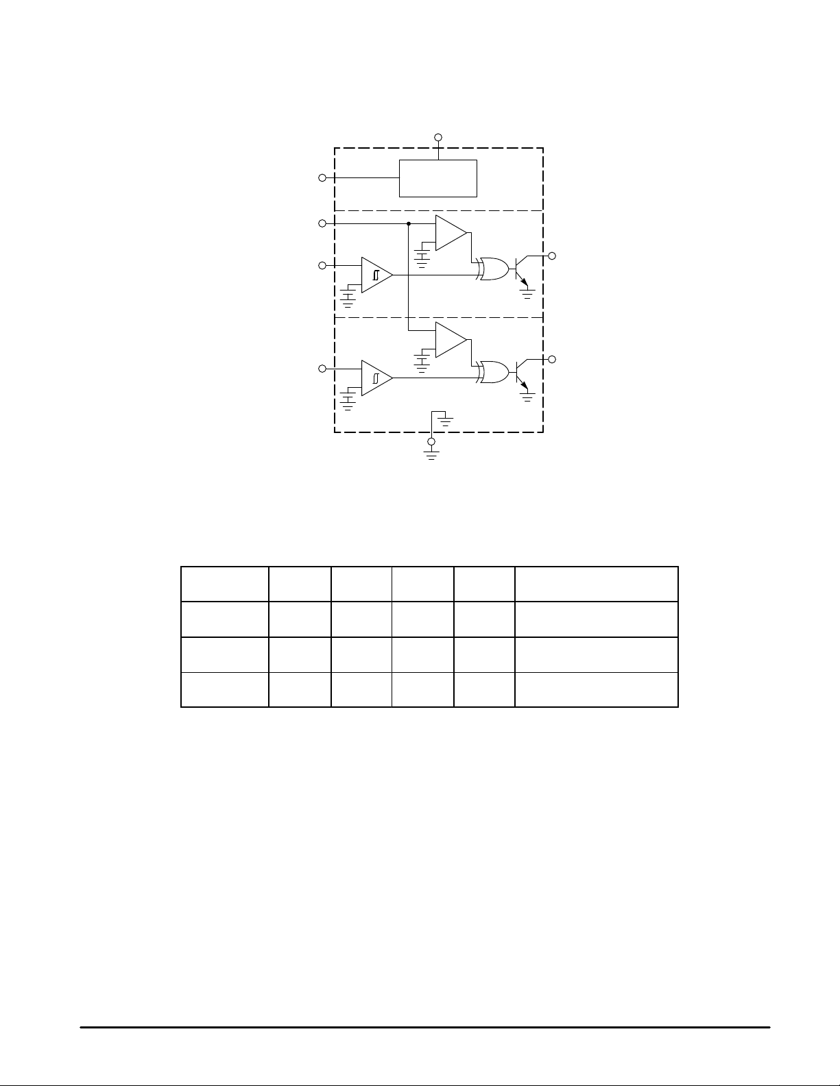
Figure 13. MC34161 Representative Block Diagram
V
CC
8
V
ref
Mode Select
Input 1
Input 2
2.54V
1
7
+
2
3
–
+
1.27V
+
–
+
1.27V
Reference
+
2.8V
+
0.6V
Gnd
–
+
–
+
4
Channel 1
Output 1
6
Channel 2
Output 2
5
Figure 14. Truth Table
Mode Select
Pin 7
GND 0
V
ref
VCC (>2.0 V) 0
Input 1
Pin 2
Output 1
Pin 6
1
0
1
1
0
1
0
1
1
0
Input 2
Pin 3
0
1
0
1
0
1
Output 2
Pin 5
0
1
1
0
1
0
Comments
Channels 1 & 2: Noninverting
Channel 1: Noninverting
Channel 2: Inverting
Channels 1 & 2: Inverting
MOTOROLA ANALOG IC DEVICE DATA
5
Page 6

MC34161 MC33161
FUNCTIONAL DESCRIPTION
Introduction
To be competitive in today’s electronic equipment market,
new circuits must be designed to increase system reliability
with minimal incremental cost. The circuit designer can take a
significant step toward attaining these goals by implementing
economical circuitry that continuously monitors critical circuit
voltages and provides a fault signal in the event of an
out–of–tolerance condition. The MC34161, MC33161 series
are universal voltage monitors intended for use in a wide
variety of voltage sensing applications. The main objectives
of this series was to configure a device that can be used in as
many voltage sensing applications as possible while
minimizing cost. The flexibility objective is achieved by the
utilization of a unique Mode Select input that is used in
conjunction with traditional circuit building blocks. The cost
objective is achieved by processing the device on a standard
Bipolar Analog flow, and by limiting the package to eight pins.
The device consists of two comparator channels each with
hysteresis, a mode select input for channel programming, a
pinned out reference, and two open collector outputs. Each
comparator channel can be configured as either inverting or
noninverting by the Mode Select input. This allows a single
device to perform over, under, and window detection of
positive and negative voltages. A detailed description of each
section of the device is given below with the representative
block diagram shown in Figure 13.
Input Comparators
The input comparators of each channel are identical, each
having an upper threshold voltage of 1.27 V ±2.0% with 25
mV of hysteresis. The hysteresis is provided to enhance
output switching by preventing oscillations as the comparator
thresholds are crossed. The comparators have an input bias
current of 60 nA at their threshold which approximates a
21.2 MΩ resistor to ground. This high impedance minimizes
loading of the external voltage divider for well defined trip
points. For all positive voltage sensing applications, both
comparator channels are fully functional at a VCC of 2.0 V . In
order to provide enhanced device ruggedness for hostile
industrial environments, additional circuitry was designed
into the inputs to prevent device latch–up as well as to
suppress electrostatic discharges (ESD).
Reference
The 2.54 V reference is pinned out to provide a means for
the input comparators to sense negative voltages, as well as
a means to program the Mode Select input for window
detection applications. The reference is capable of sourcing
in excess of 2.0 mA output current and has built–in short
circuit protection. The output voltage has a guaranteed
tolerance of ±2.4% at room temperature.
The 2.54 V reference is derived by gaining up the internal
1.27 V reference by a factor of two. With a power supply
voltage of 4.0 V, the 2.54 V reference is in full regulation,
allowing the device to accurately sense negative voltages.
Mode Select Circuit
The key feature that allows this device to be flexible is the
Mode Select input. This input allows the user to program
each of the channels for various types of voltage sensing
applications. Figure 14 shows that the Mode Select input has
three defined states. These states determine whether
Channel 1 and/or Channel 2 operate in the inverting or
noninverting mode. The Mode Select thresholds are shown in
Figure 5. The input circuitry forms a tristate switch with
thresholds at 0.63 V and V
current is 10 µA when connected to the reference output, and
42 µA when connected to a VCC of 5.0 V, refer to Figure 6.
Output Stage
The output stage uses a positive feedback base boost
circuit for enhanced sink saturation, while maintaining a
relatively low device standby current. Figure 10 shows that
the sink saturation voltage is about 0.2 V at 8.0 mA over
temperature. By combining the low output saturation
characteristics with low voltage comparator operation, this
device is capable of sensing positive voltages at a VCC of
1.0 V. These characteristics are important in undervoltage
sensing applications where the output must stay in a low
state as VCC approaches ground. Figure 4 shows the Output
Voltage versus Supply Voltage in an undervoltage sensing
application. Note that as VCC drops below the programmed
4.5 V trip point, the output stays in a well defined active low
state until VCC drops below 1.0 V.
+ 0.23 V . The mode select input
ref
APPLICATIONS
The following circuit figures illustrate the flexibility of this
device. Included are voltage sensing applications for over,
under, and window detectors, as well as three unique
configurations. Many of the voltage detection circuits are
shown with the open collector outputs of each channel
connected together driving a light emitting diode (LED). This
‘ORed’ connection is shown for ease of explanation and it is
only required for window detection applications. Note that
6
many of the voltage detection circuits are shown with a
dashed line output connection. This connection gives the
inverse function of the solid line connection. For example, the
solid line output connection of Figure 15 has the LED ‘ON’
when input voltage VS is above trip voltage V2, for
overvoltage detection. The dashed line output connection
has the LED ‘ON’ when VS is below trip voltage V2, for
undervoltage detection.
MOTOROLA ANALOG IC DEVICE DATA
Page 7

MC34161 MC33161
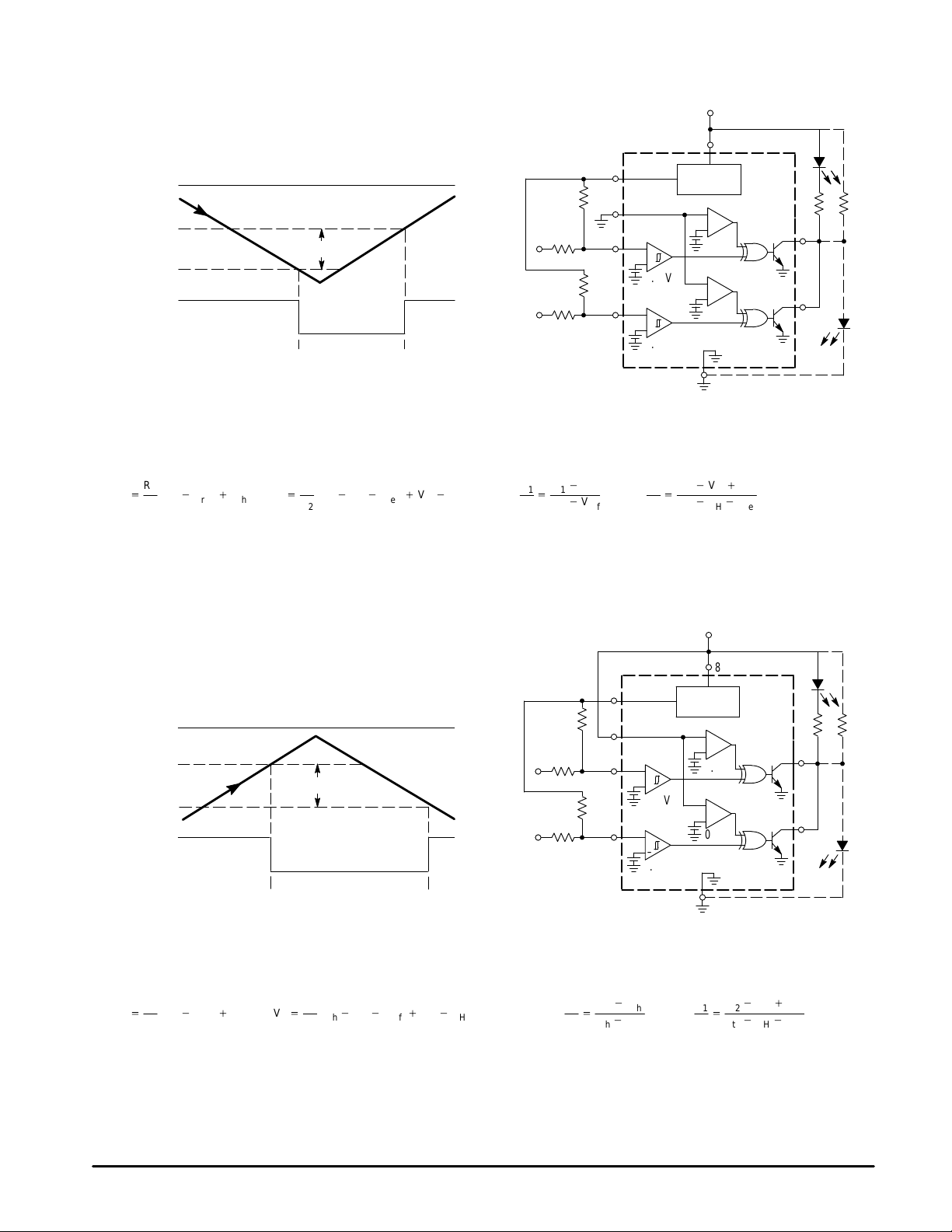
Figure 15. Dual Postive Overvoltage Detector
V
CC
V
Input V
S
Output
Voltage
Pins 5, 6
V
Gnd
V
CC
Gnd
2
V
Hys
1
V
V
S2
LED ‘ON’
R
R
1
S1
7
R
2
2
+
R
1
1.27V
2
3
1
+
1.27V
+
–
+
–
2.54V
Reference
–
+
+
2.8V
–
+
+
0.6V
6
5
4
The above figure shows the MC34161 configured as a dual positive overvoltage detector. As the input voltage increases from ground, the LED will turn ‘ON’ when
VS1 or VS2 exceeds V2. With the dashed line output connection, the circuit becomes a dual positive undervoltage detector. As the input voltage decreases from the
peak towards ground, the LED will turn ‘ON’ when VS1 or VS2 falls below V1.
For known resistor values, the voltage trip points are: For a specific trip voltage, the required resistor ratio is:
8
R
2
ǒ
V
+
(Vth*
1
VH)
Ǔ
)
1
R
1
V2+
R
2
ǒ
V
th
Ǔ
)
1
R
1
R
R
V
2
1
+
Vth*
1
*
1
V
H
R
V
2
2
+
*
R
1
1
V
th
Figure 16. Dual Postive Undervoltage Detector
V
CC
8
+
–
+
–
2.54V
Reference
–
+
+
2.8V
–
+
+
0.6V
4
R
V
2
+
R
V
1
6
5
2
*
1
th
V
2
Input V
S
Output
Voltage
Pins 5, 6
V
Gnd
V
CC
Gnd
1
V
Hys
LED ‘ON’
V
V
S2
R
R
The above figure shows the MC34161 configured as a dual positive undervoltage detector. As the input voltage decreases towards ground, the LED will turn ‘ON’
when VS1 or VS2 falls below V1. With the dashed line output connection, the circuit becomes a dual positive overvoltage detector. As the input voltage increases from
ground, the LED will turn ‘ON’ when VS1 or VS2 exceeds V2.
For known resistor values, the voltage trip points are: For a specific trip voltage, the required resistor ratio is:
R
2
ǒ
V
+
(Vth*
1
VH)
Ǔ
)
1
R
1
V2+
R
2
ǒ
V
th
Ǔ
)
1
R
1
R
R
V
2
+
Vth*
1
1
S1
7
R
2
2
+
R
1
1.27V
2
3
1
1
V
+
1.27V
*
1
H
MOTOROLA ANALOG IC DEVICE DATA
7
Page 8
MC34161 MC33161
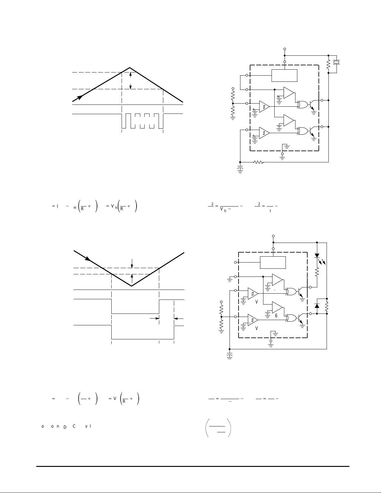
Figure 17. Dual Negative Overvoltage Detector
V
CC
8
2.54V
+
–
1.27V
+
–
1.27V
R
1
+
R
2
Reference
–
+
+
2.8V
–
+
+
0.6V
4
V
*
Vth)
2
Vth*
VH*
6
5
V
H
V
ref
Gnd
R
V
1
Input –V
S
V
2
Output
Voltage
Pins 5, 6
The above figure shows the MC34161 configured as a dual negative overvoltage detector . As the input voltage increases from ground, the LED will turn ‘ON’ when
–VS1 or –VS2 exceeds V2. With the dashed line output connection, the circuit becomes a dual negative undervoltage detector. As the input voltage decreases from
the peak towards ground, the LED will turn ‘ON’ when –VS1 or –VS2 falls below V1.
For known resistor values, the voltage trip points are: For a specific trip voltage, the required resistor ratio is:
V1+
R
R
V
CC
Gnd
1
(Vth*
2
V
))V
ref
thV2
V
Hys
LED ‘ON’
R
1
+
(Vth*
VH*
V
))Vth*
R
2
ref
V
H
–V
S2
R
R
–V
1
2
+
S1
R1
R
R1
V
1
Vth*
1
2
7
2
+
2
3
+
*
V
th
V
ref
Figure 18. Dual Negative Undervoltage Detector
V
CC
8
2.54V
+
–
1.27V
+
–
1.27V
Reference
–
+
+
2.8V
–
+
+
0.6V
4
V
R
1
+
R
Vth*
2
6
5
*
Vth)
VH*
V
H
V
ref
2
1
2
7
2
+
2
3
+
V
R
R
*
+
1
Vth*
V
th
V
ref
1
2
S2
–V
R
R1
S1
R
R1
Gnd
V
1
V
V2+
R
R
Hys
1
(Vth*
2
LED ‘ON’
VH*
V
ref
))Vth*
–V
V
H
Input –V
S
V
2
Output
Voltage
Pins 5, 6
The above figure shows the MC34161 configured as a dual negative undervoltage detector. As the input voltage decreases towards ground, the LED will turn ‘ON’
when –VS1 or –VS2 falls below V1. With the dashed line output connection, the circuit becomes a dual negative overvoltage detector. As the input voltage increases
from ground, the LED will turn ‘ON’ when –VS1 or –VS2 exceeds V2.
For known resistor values, the voltage trip points are: For a specific trip voltage, the required resistor ratio is:
V1+
R
R
V
CC
Gnd
1
(Vth*
2
V
))V
ref
th
8
MOTOROLA ANALOG IC DEVICE DATA
Page 9

MC34161 MC33161
Figure 19. Positive V oltage W indow Detector
V
CC
8
+
–
+
–
2.54V
Reference
–
+
+
2.8V
–
+
+
0.6V
6
5
Input V
S
Output
Voltage
Pins 5, 6
CH2
CH1
Gnd
V
CC
Gnd
V
4
V
3
V
2
V
1
V
Hys2
V
Hys1
LED ‘ON’
V
1
S
7
R
3
2
+
R
2
1.27V
LED ‘ON’‘OFF’LED ‘OFF’‘ON’
3
R
1
+
1.27V
4
The above figure shows the MC34161 configured as a positive voltage window detector. This is accomplished by connecting channel 1 as an undervoltage detector ,
and channel 2 as an overvoltage detector. When the input voltage VS falls out of the window established by V1 and V4, the LED will turn ‘ON’. As the input voltage
falls within the window, VS increasing from ground and exceeding V2, or VS decreasing from the peak towards ground and falling below V3, the LED will turn ‘OFF’.
With the dashed line output connection, the LED will turn ‘ON’ when the input voltage VS is within the window.
For known resistor values, the voltage trip points are: For a specific trip voltage, the required resistor ratio is:
V1+
V2+
*
ǒ
R1)
VH1)
R
ǒ
3
R
2
R1)
)
)
1ǓV3+
R
2
Ǔ
1
V4+
(V
th2
ǒ
V
th2
(V
th1
V
th1
R
3
*
R2)
VH2)
R
R2)
R
3
ǒ
R
R
3
)
1
1
Ǔ
)
1
1
Ǔ
R
R
R
R
2
+
1
2
+
1
V
3(Vth2
V
1(Vth1
V
4xVth2
V2xV
R
*
VH2)
*
VH1)
*
1
1
*
th1
V
*
V
)
3
3(V1
+
R
V
1
1(Vth2
R
V
+
*
4(V2
V2xV
3
R
1
VH1)
th1
*
VH2)
V
)
th1
th2
V
Figure 20. Negative V oltage Window Detector
CC
8
2.54V
3
2
1
–V
R2)
R2)
R1)
R1)
1
7
2
+
3
+
S
R
R
R
R
V
1
1
+
R
V
3
th2
V
1
2
+
R
V
3
th2
V
3
th1
+
R
V3*
2
V
3
th1
+
R
V4)
2
Gnd
V
1
CH2
V
R
R
(R
(R
CH1
1(Vth2
R
2
1(Vth2
)
1
)
1
V
V
V
CC
Gnd
*
)
*
R
R2)(V
R2)(V
2
3
4
R
)
2
R
V
)
ref
3
VH2*
R
3
th1
3
th1
R
3
)
*
*
V
th2
V
)
ref
V
ref
VH1*
V
Hys1
)
V
)
)
V
V
Input –V
S
Output
Voltage
Pins 5, 6
The above figure shows the MC34161 configured as a negative voltage window detector. When the input voltage –VS falls out of the window established by V1 and
V4, the LED will turn ‘ON’. As the input voltage falls within the window, –VS increasing from ground and exceeding V2, or –VS decreasing from the peak towards ground
and falling below V3, the LED will turn ‘OFF’. With the dashed line output connection, the LED will turn ‘ON’ when the input voltage –VS is within the window.
For known resistor values, the voltage trip points are: For a specific trip voltage, the required resistor ratio is:
V1+
V2+
V3+
V4+
V
Hys2
R
R
LED ‘ON’ LED ‘ON’‘OFF’LED ‘OFF’‘ON’
*
V
th2
H2
th1
)
ref
)
V
*
V
th1
H1
R
+
–
1.27V
+
–
1.27V
*
V
th2
*
V
*
V
th2
*
VH2*
*
V
V
th1
*
VH1*
VH1*
Reference
+
+
4
ref
)
V
V
ref
V
V
2.8V
0.6V
H2
ref
ref
th1
–
+
6
–
+
5
MOTOROLA ANALOG IC DEVICE DATA
9
Page 10

MC34161 MC33161
Figure 21. Positive and Negative Overvoltage Detector
V
CC
8
V
S2
4
V
3
Input V
Gnd
V
S1
R
R
R
R
3
4
3
4
V
Gnd
(V
(V
V
CC
th1
th1
1
2
*
V
))V
ref
th1
*
VH1*
V
))V
ref
th1
Input –V
Output
Voltage
Pins 5, 6
The above figure shows the MC34161 configured as a positive and negative overvoltage detector. As the input voltage increases from ground, the LED will turn ‘ON’
when either –VS1 exceeds V2, or VS2 exceeds V4. With the dashed line output connection, the circuit becomes a positive and negative undervoltage detector. As the
input voltage decreases from the peak towards ground, the LED will turn ‘ON’ when either VS2 falls below V3, or –VS1 falls below V1.
For known resistor values, the voltage trip points are: For a specific trip voltage, the required resistor ratio is:
V1+
V2+
V
Hys2
1
7
R
–V
V
Hys1
LED ‘ON’
R
2
V3+
(V
th2
*
V
H1
V4+
V
th2
ǒ
*
VH2)
R
2
ǒ
R
1
)
1
R
1
Ǔ
)
1
S1
V
S2
Ǔ
R
R2
4
+
2
–
3
R
+
1.27V
+
3
–
+
1
R
R
R
R
1.27V
(V
*
3
1
+
(V
4
th1
(V
*
3
2
+
(V
4
th1
V
*
V
*
Reference
)
th1
V
)
ref
)
th1
VH1*
2.54V
+
+
4
VH1)
V
–
+
2.8V
–
+
0.6V
ref
6
5
V
R
2
4
+
*
R
1
R
2
)
+
R
1
1
V
th2
V
3
V
th2
*
*
V
H2
1
Figure 22. Positive and Negative Undervoltage Detector
V
CC
8
V
S1
2
V
1
Input V
Gnd
V
S2
V
Gnd
(V
V
th1
V
CC
th1
3
4
R
4
ǒ
*
VH1)
R
4
ǒ
)
1
R
3
Ǔ
)
1
R
3
Ǔ
V3+
V4+
Input –V
Output
Voltage
Pins 5, 6
The above figure shows the MC34161 configured as a positive and negative undervoltage detector. As the input voltage decreases toward ground, the LED will turn
‘ON’ when either VS1 falls below V1, or –VS2 falls below V3. With the dashed line output connection, the circuit becomes a positive and negative overvoltage detector.
As the input voltage increases from the ground, the LED will turn ‘ON’ when either VS1 exceeds V2, or –VS1 exceeds V1.
For known resistor values, the voltage trip points are: For a specific trip voltage, the required resistor ratio is:
V1+
V2+
R
R
R
R
V
V
1
(Vth*
2
1
(Vth*
2
Hys1
Hys2
LED ‘ON’
V
VH2*
ref
))V
1
7
R
4
V
S1
R
3
R
2
R
1
–V
S2
th2
V
))V
*
th2
V
H2
ref
R
R
R
R
+
2
–
+
1.27V
+
3
–
+
1.27V
V
4
2
+
*
V
3
th1
V
4
+
V
*
3
th1
1
1
V
Reference
+
+
4
*
H1
2.54V
–
+
2.8V
–
+
0.6V
1
6
5
V
)
VH2*
*
*
VH2*
V
th2
V
ref
V
th2
V
ref
R
1
4
+
R
V
2
th2
V
R
R
*
1
3
+
V
2
th2
10
MOTOROLA ANALOG IC DEVICE DATA
Page 11
MC34161 MC33161
Figure 23. Overvoltage Detector with Audio Alarm
V
CC
Input V
S
Output
Voltage
Pins 5, 6
V
V
Gnd
V
CC
Gnd
8
2
V
Hys
1
R
R
1
V
S
7
2
1
+
2
–
+
1.27V
Osc ‘ON’
+
3
–
+
2.54V
Reference
–
+
+
2.8V
–
+
+
0.6V
R
A
Piezo
6
5
1.27V
4
C
T
The above figure shows the MC34161 configured as an overvoltage detector with an audio alarm. Channel 1 monitors input voltage VS while channel 2 is connected
as a simple RC oscillator. As the input voltage increases from ground, the output of channel 1 allows the oscillator to turn ‘ON’ when VS exceeds V2.
For known resistor values, the voltage trip points are: For a specific trip voltage, the required resistor ratio is:
V1+
(Vth*
VH)
R
2
ǒ
)
1ǓV2+
R
1
R
2
ǒ
V
th
Ǔ
)
1
R
1
R
R
V
2
1
+
Vth*
1
V
H
Figure 24. Microprocessor Reset with Time Delay
R
B
R
V
2
*
1
2
+
*
R
1
1
V
th
V
CC
8
2.54V
Input V
V
2
S
V
1
V
Hys
1
7
Gnd
2
V
Output
Voltage
Pin 5
Output
Voltage
Pin 6
The above figure shows the MC34161 configured as a microprocessor reset with a time delay. Channel 2 monitors input voltage VS while channel 1 performs the time
delay function. As the input voltage decreases towards ground, the output of channel 2 quickly discharges C
from ground, the output of channel 2 allows R
For known resistor values, the voltage trip points are: For a specific trip voltage, the required resistor ratio is:
For known R
V1+
V
CC
Gnd
V
CC
Gnd
(Vth*
DLY CDLY
R
2
ǒ
VH)
)
1ǓV2+
R
1
values, the reset time delay is:
Reset LED ‘ON’
DLY
R
2
ǒ
V
)
th
R
1
to charge C
Ǔ
1
t
DLY
when VS exceeds V2.
DLY
t
= R
DLY
DLYCDLY
In
S
R
2
R
1
R
2
+
R
Vth*
1
1
V
th
1 –
V
CC
+
3
+
C
DLY
DLY
V
1
*
V
H
Reference
R
3
6
R
DLY
5
+
–
1.27V
+
–
–
+
+
2.8V
–
+
+
0.6V
1.27V
4
when VS falls below V1. As the input voltage increases
R
V
2
1
2
+
*
R
1
1
V
th
MOTOROLA ANALOG IC DEVICE DATA
11
Page 12

Input
92 Vac to
276 Vac
MC34161 MC33161
Figure 25. Automatic AC Line Voltage Selector
B+
+
MAC
228A6FP
3.0A
MR506
8
2.54V
1
Reference
10k
1.2k
T
220
250V
+
220
250V
75k
75k
RTN
10k
100k
1.6M
10k
3W
+
47
1N
4742
The above circuit shows the MC34161 configured as an automatic line voltage selector. The IC controls the triac, enabling the circuit to function
as a fullwave voltage doubler or a fullwave bridge. Channel 1 senses the negative half cycles of the AC line voltage. If the line voltage is less
than150 V , the circuit will switch from bridge mode to voltage doubling mode after a preset time delay. The delay is controlled by the 100 kΩ resistor
and the 10 µF capacitor. If the line voltage is greater than 150V, the circuit will immediately return to fullwave bridge mode.
7
+
2
–
+
1.27V
+
3
–
+
10
1.27V
+
–
+
+
2.8V
–
+
+
0.6V
4
6
5
12
MOTOROLA ANALOG IC DEVICE DATA
Page 13
V
in
12V
330
MC34161 MC33161
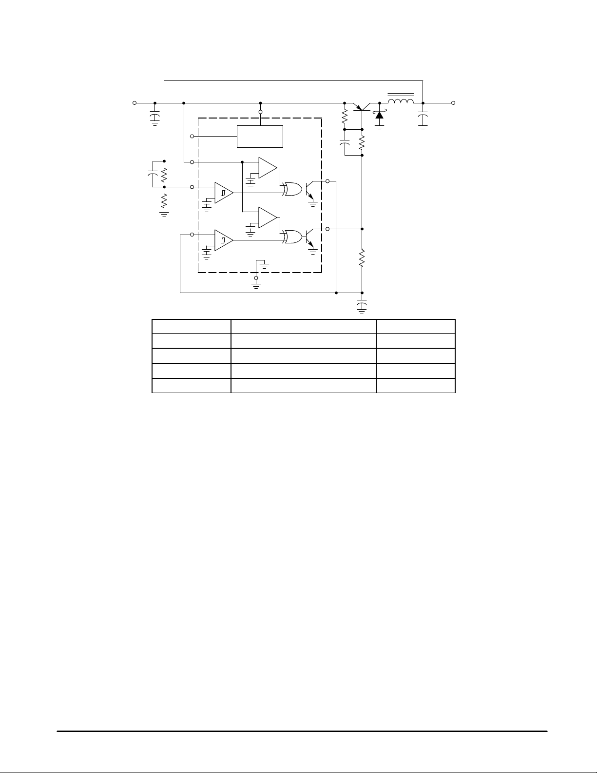
Figure 26. Step–Down Converter
470µH
470
0.01
MPS750
1.8k
1N5819
+
+
1
8
2.54V
Reference
1000
V
O
5.0V/250mA
0.01
Line Regulation Vin = 9.5 V to 24 V, IO = 250 mA 40 mV = ±0.1%
Load Regulation Vin = 12 V, IO = 0.25 mA to 250 mA 2.0 mV = ±0.2%
Output Ripple Vin = 12 V, IO = 250 mA 50 mVpp
Efficiency Vin = 12 V, IO = 250 mA 87.8%
The above figure shows the MC34161 configured as a step–down converter. Channel 1 monitors the output voltage while Channel 2
performs the oscillator function. Upon initial power–up, the converters output voltage will be below nominal, and the output of Channel
1 will allow the oscillator to run. The external switch transistor will eventually pump–up the output capacitor until its voltage exceeds the
input threshold of Channel 1. The output of Channel 1 will then switch low and disable the oscillator. The oscillator will commence
operation when the output voltage falls below the lower threshold of Channel 1.
7
4.7k
+
2
–
1.6k
+
1.27V
+
3
–
+
1.27V
Test Conditions Results
–
+
+
2.8V
–
+
+
0.6V
4
6
5
47k
0.005
MOTOROLA ANALOG IC DEVICE DATA
13
Page 14

NOTE 2
A
E
B
C
A1
–T–
SEATING
PLANE
H
58
14
F
–A–
N
D
G
0.13 (0.005) B
D
58
1
H
4
e
B
SS
–B–
C
M
0.25MB
A
SEATING
PLANE
A0.25MCB
MC34161 MC33161
OUTLINE DIMENSIONS
P SUFFIX
PLASTIC PACKAGE
CASE 626–05
ISSUE K
L
J
K
0.10
A
T
M
M
M
M
D SUFFIX
PLASTIC PACKAGE
CASE 751–06
(SO–8)
ISSUE T
h
X 45
_
q
NOTES:
1. DIMENSION L TO CENTER OF LEAD WHEN
FORMED PARALLEL.
2. PACKAGE CONTOUR OPTIONAL (ROUND OR
SQUARE CORNERS).
3. DIMENSIONING AND TOLERANCING PER ANSI
Y14.5M, 1982.
DIM MIN MAX MIN MAX
A 9.40 10.16 0.370 0.400
B 6.10 6.60 0.240 0.260
C 3.94 4.45 0.155 0.175
D 0.38 0.51 0.015 0.020
F 1.02 1.78 0.040 0.070
G 2.54 BSC 0.100 BSC
H 0.76 1.27 0.030 0.050
J 0.20 0.30 0.008 0.012
K 2.92 3.43 0.115 0.135
L 7.62 BSC 0.300 BSC
M ––– 10 ––– 10
N 0.76 1.01 0.030 0.040
NOTES:
C
L
1. DIMENSIONING AND TOLERANCING PER ASME
Y14.5M, 1994.
2. DIMENSIONS ARE IN MILLIMETER.
3. DIMENSION D AND E DO NOT INCLUDE MOLD
PROTRUSION.
4. MAXIMUM MOLD PROTRUSION 0.15 PER SIDE.
5. DIMENSION B DOES NOT INCLUDE DAMBAR
PROTRUSION. ALLOWABLE DAMBAR
PROTRUSION SHALL BE 0.127 TOTAL IN EXCESS
OF THE B DIMENSION AT MAXIMUM MATERIAL
CONDITION.
MILLIMETERS
DIM MIN MAX
A 1.35 1.75
A1 0.10 0.25
B 0.35 0.49
C 0.19 0.25
D 4.80 5.00
E
3.80 4.00
1.27 BSCe
H 5.80 6.20
h
0.25 0.50
L 0.40 1.25
0 7
q
INCHESMILLIMETERS
__
__
14
MOTOROLA ANALOG IC DEVICE DATA
Page 15

MC34161 MC33161
Motorola reserves the right to make changes without further notice to any products herein. Motorola makes no warranty , representation or guarantee regarding
the suitability of its products for any particular purpose, nor does Motorola assume any liability arising out of the application or use of any product or circuit, and
specifically disclaims any and all liability, including without limitation consequential or incidental damages. “T ypical” parameters which may be provided in Motorola
data sheets and/or specifications can and do vary in different applications and actual performance may vary over time. All operating parameters, including “Typicals”
must be validated for each customer application by customer’s technical experts. Motorola does not convey any license under its patent rights nor the rights of
others. Motorola products are not designed, intended, or authorized for use as components in systems intended for surgical implant into the body, or other
applications intended to support or sustain life, or for any other application in which the failure of the Motorola product could create a situation where personal injury
or death may occur. Should Buyer purchase or use Motorola products for any such unintended or unauthorized application, Buyer shall indemnify and hold Motorola
and its officers, employees, subsidiaries, affiliates, and distributors harmless against all claims, costs, damages, and expenses, and reasonable attorney fees
arising out of, directly or indirectly, any claim of personal injury or death associated with such unintended or unauthorized use, even if such claim alleges that Motorola
was negligent regarding the design or manufacture of the part. Motorola and are registered trademarks of Motorola, Inc. Motorola, Inc. is an Equal
Opportunity/Affirmative Action Employer.
MOTOROLA ANALOG IC DEVICE DATA
15
Page 16

MC34161 MC33161
How to reach us:
USA/EUROPE/Locations Not Listed: Motorola Literature Distribution; JAPAN: Nippon Motorola Ltd.: SPD, Strategic Planning Office, 141,
P.O. Box 5405, Denver, Colorado 80217. 1–303–675–2140 or 1–800–441–2447 4–32–1 Nishi–Gotanda, Shagawa–ku, Tokyo, Japan. 03–5487–8488
Customer Focus Center: 1–800–521–6274
Mfax: RMFAX0@email.sps.mot.com – TOUCHTONE 1–602–244–6609 ASIA/PACIFIC: Motorola Semiconductors H.K. Ltd.; 8B Tai Ping Industrial Park,
Moto rola Fa x Back Syst em – US & Canada ONLY 1–800–774–1848 51 Ting Kok Road, Tai Po, N.T., Hong Kong. 852–26629298
HOME PAGE: http://motorola.com/sps/
16
– http://sps.motorola.com/mfax/
◊
MOTOROLA ANALOG IC DEVICE DATA
Mfax is a trademark of Motorola, Inc.
MC34161/D
 Loading...