

Page 1
SEMICONDUCTOR
TECHNICAL DATA
28–CHANNEL
INKJET DRIVER
(SMARTMOS Technology)
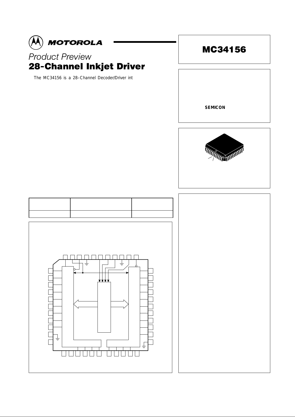
Pin No.
1
2
3
4
5
6
7
8
9
10
11
12
13
14
15
16
17
18
19
20
21
22
23
24
25
26
27
28
29
30
31
32
33
34
35
36
37
38
39
40
41
42
43
44
Pin Name
IND
V
DD
Gnd
ENB
Chip Enable
OUTB0
OUTB1
OUTB2
OUTB3
OUTB4
OUTB5
OUTB6
OUTB7
OUTB8
OUTB9
Gnd
N/C
N/C
N/C
OUTB10
OUTB11
OUTB12
OUTB13
OUTA13
OUTA12
OUTA11
OUTA10
COM
Gnd
OUTA9
OUTA8
OUTA7
OUTA6
OUTA5
OUTA4
OUTA3
OUTA2
OUTA1
OUTA0
ENA
INA
Gnd
INB
INC
Pin Description
4th Decoder Input
Power Supply
Ground
Enable Pin for B Set Drivers
Chip Enable
B Set 1st Driver
B Set 2nd Driver
B Set 3rd Driver
B Set 4th Driver
B Set 5th Driver
B Set 6th Driver
B Set 7th Driver
B Set 8th Driver
B Set 9th Driver
B Set 10th Driver
Ground
Not Connected
Not Connected
Not Connected
B Set 11th Driver
B Set 12th Driver
B Set 13th Driver
B Set 14th Driver
A Set 14th Driver
A Set 13th Driver
A Set 12th Driver
A Set 11th Driver
Common
Ground
A Set 10th Driver
A Set 9th Driver
A Set 8th Driver
A Set 7th Driver
A Set 6th Driver
A Set 5th Driver
A Set 4th Driver
A Set 3rd Driver
A Set 2nd Driver
A Set 1st Driver
Enable Pin for A Set Drivers
1st Decoder Input
Ground
2nd Decoder Input
3rd Decoder Input
FN SUFFIX
PLASTIC PACKAGE
CASE 777
44
1
PIN ASSIGNMENTS
Order this document from Analog Marketing
1
MOTOROLA ANALOG IC DEVICE DATA
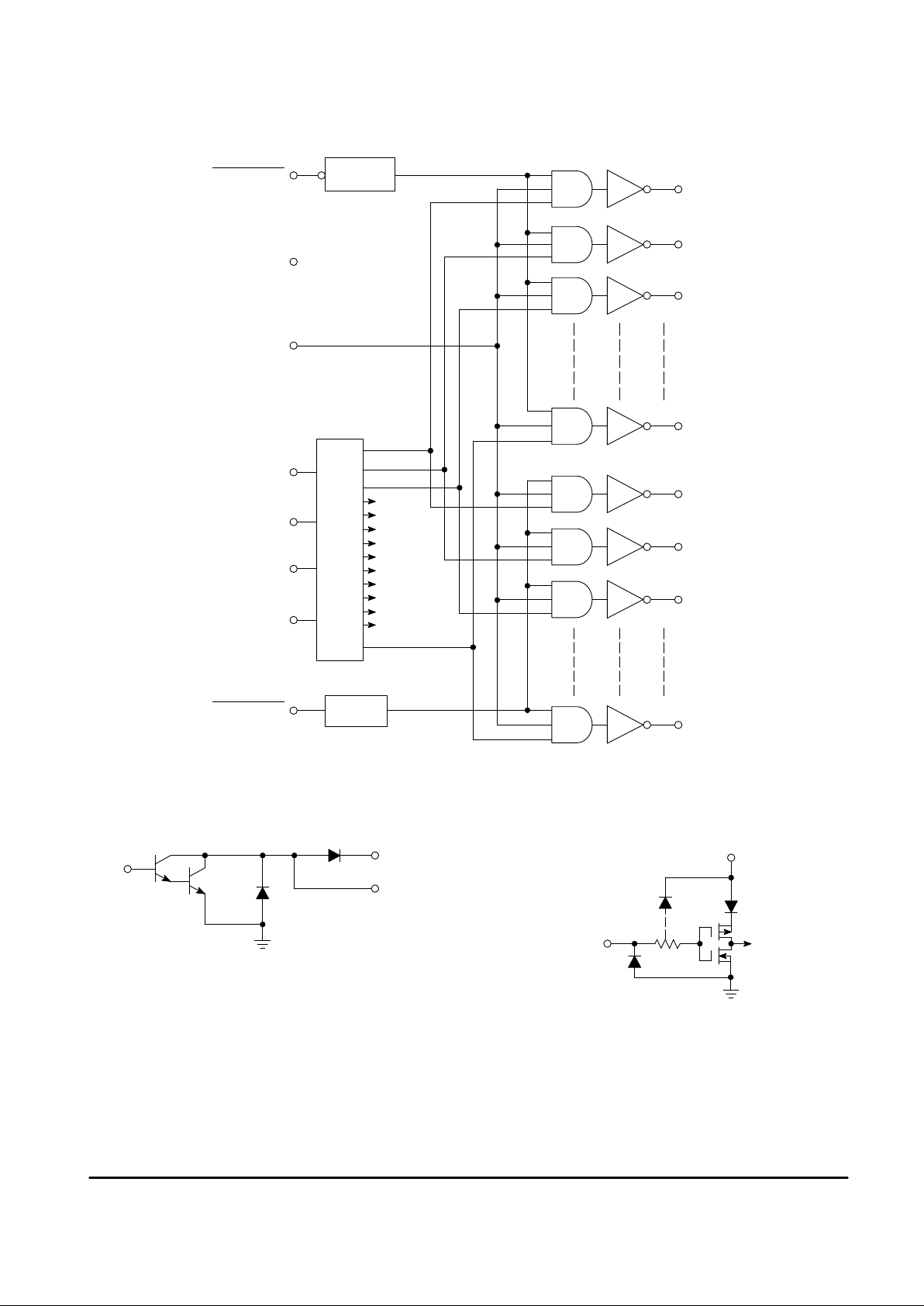
The MC34156 is a 28–Channel Decoder/Driver intended to be used in
inkjet printer applications. By using sophisticated SMARTMOS technology, it
has been possible to combine low power CMOS inputs and logic and high
current, high voltage bipolar outputs capable of sustaining a maximum of 30 V .
A 4–to–14 line decoder determines the selected output driver (n) in each
14–driver bank. Two independent output enable inputs (active low) then
provide the final decoding to activate 1– or 2–of–28 outputs (OUTAn and/or
OUTBn). The ac electrical characteristics of the drivers are tightly controlled
and thereby the energy of the device delivers to the inkjet print head. A Chip
Enable function is provided to lock out the drivers during system power up.
The 28 bipolar power outputs are open collector 30 V Darlington drivers
capable of sinking 500 mA at ambient temperatures up to 70°C. All driver
outputs are capable of withstanding a contact discharge of ±8.0 kV with the
IC biased.
• ESD Output Protection with Clamping Diodes
• Addressable Data Entry
• Tightly Controlled AC and Electrical Characteristics for Inkjet Printers
• CMOS, TTL Compatible Inputs
• Low Power CMOS Logic
SMARTMOS is a trademark of Motorola, Inc.
ORDERING INFORMATION
Device
Operating
Temperature Range
Package
MC34156FN TA = 0° to +70°C Plastic Package
Simplified Block Diagram
OUTB1 OUTA0
OUTB2 OUTA1
OUTB3 OUTA2
OUTB4 OUTA3
OUTB5 OUTA4
OUTB6 OUTA5
OUTB7 OUTA6
OUTB8 OUTA7
OUTB9 OUTA8
Gnd OUTA9
N/C Gnd
7
8
9
10
11
12
13
14
15
16
17
39
38
37
36
35
34
33
32
31
30
29
6
5
4
3
2
1
44
43
42
41
40
18
19
20
21
22
23
24
25
26
27
28
OUTB0
N/C
Chip Enable
Output Enable B
Gnd
Logic Supply
IND (MSB)
INC
INB
Gnd
INA (LSB)
Output Enable A
N/C
OUTB10
OUTB11
OUTB12
OUTB13
OUTA13
OUTA12
OUTA11
OUTA10
COM
Output Driver Bank B
4–T o–14 Line Decoder
Output Driver Bank A
V
DD
This document contains information on a product under development. Motorola reserves the
right to change or discontinue this product without notice.
Motorola, Inc. 1996 Issue 0
Page 2
MC34156
2
MOTOROLA ANALOG IC DEVICE DATA
OUTA0
OUTA1
OUTA2
OUTA13
OUTB0
OUTB1
OUTB2
OUTB13
Output Enable A
Logic Supply
Chip Enable
INA (LSB)
INB
INC
IND (MSB)
Output Enable B
Turn Off
Delay
Turn On
Delay
4–to–14 Line Decoder
Figure 1. Functional Block Diagram
Figure 2. Output Driver Configuration Figure 3. Typical Input Circuit
COM
OUT
V
DD
IN
Page 3

MC34156
3
MOTOROLA ANALOG IC DEVICE DATA
FN SUFFIX
PLASTIC PACKAGE
CASE 777–02
ISSUE C
OUTLINE DIMENSIONS
NOTES:
1. DATUMS –L–, –M–, AND –N– ARE DETERMINED WHERE TOP OF LEAD
SHOULDER EXITS PLASTIC BODY AT MOLD PARTING LINE.
2. DIMENSION G1, TRUE POSITION TO BE MEASURED AT DATUM –T–,
SEATING PLANE.
3. DIMENSIONS R AND U DO NOT INCLUDE MOLD FLASH. ALLOWABLE MOLD
FLASH IS 0.010 (0.25) PER SIDE.
4. DIMENSIONING AND TOLERANCING PER ANSI Y14.5M, 1982.
5. CONTROLLING DIMENSION: INCH.
6. THE PACKAGE TOP MAY BE SMALLER THAN THE PACKAGE BOTTOM BY
UP TO 0.012 (0.300). DIMENSIONS R AND U ARE DETERMINED AT THE
OUTERMOST EXTREMES OF THE PLASTIC BODY EXCLUSIVE OF MOLD
FLASH, TIE BAR BURRS, GATE BURRS AND INTERLEAD FLASH, BUT
INCLUDING ANY MISMATCH BETWEEN THE TOP AND BOTTOM OF THE
PLASTIC BODY.
7. DIMENSION H DOES NOT INCLUDE DAMBAR PROTRUSION OR
INTRUSION. THE DAMBAR PROTRUSION(S) SHALL NOT CAUSE THE H
DIMENSION TO BE GREATER THAN 0.037 (0.940). THE DAMBAR
INTRUSION(S) SHALL NOT CAUSE THE H DIMENSION TO BE SMALLER
THAN 0.025 (0.635).
–N–
–L–
–M–
D
Y
D
K
V
W
144
BRK
B
Z
U
X
VIEW D–D
S
L–M
M
0.007(0.180) N
S
T
S
L–M
M
0.007(0.180) N
S
T
G1
S
L–M
S
0.010 (0.25) N
S
T
K1
F
H
S
L–M
M
0.007(0.180) N
S
T
Z
G
G1
R
A
E
J
VIEW S
C
S
L–M
M
0.007(0.180) N
S
T
S
L–M
M
0.007(0.180) N
S
T
0.004 (0.10)
–T–
SEATING
PLANE
VIEW S
DIM MIN MAX MIN MAX
MILLIMETERSINCHES
A 0.685 0.695 17.40 17.65
B 0.685 0.695 17.40 17.65
C 0.165 0.180 4.20 4.57
E 0.090 0.110 2.29 2.79
F 0.013 0.019 0.33 0.48
G 0.050 BSC 1.27 BSC
H 0.026 0.032 0.66 0.81
J 0.020 ––– 0.51 –––
K 0.025 ––– 0.64 –––
R 0.650 0.656 16.51 16.66
U 0.650 0.656 16.51 16.66
V 0.042 0.048 1.07 1.21
W 0.042 0.048 1.07 1.21
X 0.042 0.056 1.07 1.42
Y ––– 0.020 ––– 0.50
Z 2 10 2 10
G1 0.610 0.630 15.50 16.00
K1 0.040 ––– 1.02 –––
S
L–M
S
0.010 (0.25) N
S
T
S
L–M
M
0.007(0.180) N
S
T
____
Motorola reserves the right to make changes without further notice to any products herein. Motorola makes no warranty , representation or guarantee regarding
the suitability of its products for any particular purpose, nor does Motorola assume any liability arising out of the application or use of any product or circuit, and
specifically disclaims any and all liability, including without limitation consequential or incidental damages. “T ypical” parameters which may be provided in Motorola
data sheets and/or specifications can and do vary in different applications and actual performance may vary over time. All operating parameters, including “Typicals”
must be validated for each customer application by customer’s technical experts. Motorola does not convey any license under its patent rights nor the rights of
others. Motorola products are not designed, intended, or authorized for use as components in systems intended for surgical implant into the body, or other
applications intended to support or sustain life, or for any other application in which the failure of the Motorola product could create a situation where personal injury
or death may occur. Should Buyer purchase or use Motorola products for any such unintended or unauthorized application, Buyer shall indemnify and hold Motorola
and its officers, employees, subsidiaries, affiliates, and distributors harmless against all claims, costs, damages, and expenses, and reasonable attorney fees
arising out of, directly or indirectly, any claim of personal injury or death associated with such unintended or unauthorized use, even if such claim alleges that
Motorola was negligent regarding the design or manufacture of the part. Motorola and are registered trademarks of Motorola, Inc. Motorola, Inc. is an Equal
Opportunity/Affirmative Action Employer.
How to reach us:
USA/EUROPE/ Locations Not Listed: Motorola Literature Distribution; JAPAN: Nippon Motorola Ltd.; Tatsumi–SPD–JLDC, 6F Seibu–Butsuryu–Center,
P.O. Box 20912; Phoenix, Arizona 85036. 1–800–441–2447 or 602–303–5454 3–14–2 Tatsumi Koto–Ku, Tokyo 135, Japan. 03–81–3521–8315
MFAX: RMF AX0@email.sps.mot.com – TOUCHT ONE 602–244–6609 ASIA/PACIFIC: Motorola Semiconductors H.K. Ltd.; 8B Tai Ping Industrial Park,
INTERNET: http://Design–NET .com 51 Ting Ko k Road, Tai Po, N.T., Hong Kong. 852–26629298
MC34156/D
*MC34156/D*
◊
 Loading...