

Datasheet MC34084DWR2, MC34080BD, MC34080BDR2, MC34084DW, MC34083BP Datasheet (MOTOROLA)
...Page 1
$"%
HIGH PERFORMANCE
JFET INPUT
OPERATIONAL AMPLIFIERS
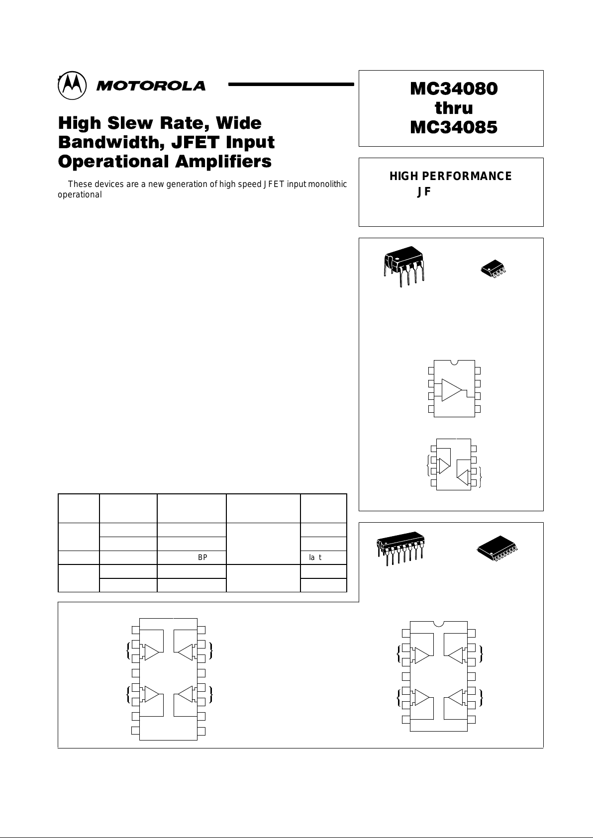
Order this document by MC34080/D
D SUFFIX
PLASTIC PACKAGE
CASE 751
(SO–8)
P SUFFIX
PLASTIC PACKAGE
CASE 626
DW SUFFIX
PLASTIC PACKAGE
CASE 751G
(SO–16L)
P SUFFIX
PLASTIC PACKAGE
CASE 646
PIN CONNECTIONS
PIN CONNECTIONS
(Single, Top View)
(Dual, Top View)
(Quad, Top View)
4
23
1
4
23
1
–
Offset Null
Noninv. Input
V
EE
Inv. Input
V
EE
Inputs 1
Output 1
NC
V
CC
Output
Offset Null
Inputs 2
Output 2
V
CC
1
2
3
4
8
7
6
5
+
1
2
3
4
8
7
6
5
–
+
–
+
Inputs 1
Output 1
V
CC
Inputs 2
Output 2
Inputs 1
Output 1
V
CC
Inputs 2
Output 2
NC
Output 4
Inputs 4
V
EE
Inputs 3
Output 3
Output 4
Inputs 4
V
EE
Inputs 3
Output 3
NC
1
2
3
4
5
6
710
11
12
13
14
15
16
8
9
1
2
3
4
5
6
78
9
10
11
12
13
14
–
+
–
+
+
–
+
–
–
+
–
+
+
–
+
–
1
8
1
8
14
1
16
1
1
MOTOROLA ANALOG IC DEVICE DATA
t
& $
&$ !%$
!"$ !"#
These devices are a new generation of high speed JFET input monolithic
operational amplifiers. Innovative design concepts along with JFET
technology provide wide gain bandwidth product and high slew rate.
Well–matched JFET input devices and advanced trim techniques ensure low
input offset errors and bias currents. The all NPN output stage features large
output voltage swing, no deadband crossover distortion, high capacitive
drive capability, excellent phase and gain margins, low open loop output
impedance, and symmetrical source/sink AC frequency response.
This series of devices is available in fully compensated or
decompensated (A
VCL
≤2) and is specified over a commercial temperature
range. They are pin compatible with existing Industry standard operational
amplifiers, and allow the designer to easily upgrade the performance of
existing designs.
• Wide Gain Bandwidth: 8.0 MHz for Fully Compensated Devices
Wide Gain Bandwidth: 16 MHz for Decompensated Devices
• High Slew Rate: 25 V/µs for Fully Compensated Devices
High Slew Rate: 50 V/µs for Decompensated Devices
• High Input Impedance: 10
12
Ω
• Input Offset Voltage: 0.5 mV Maximum (Single Amplifier)
• Large Output Voltage Swing: –14.7 V to +14 V for
Large Output Voltage Swing: VCC/VEE = ±15 V
• Low Open Loop Output Impedance: 30 Ω @ 1.0 MHz
• Low THD Distortion: 0.01%
• Excellent Phase/Gain Margins: 55°/7.6 dB for Fully Compensated
Devices
ORDERING INFORMATION
Op Amp
Function
Fully
Compen-
sated
A
VCL
≥2
Compensated
Operating
Temperature
Range
Package
MC34081BD MC34080BD
SO–8
Singl
e
MC34081BP MC34080BP
TA = 0° to +70°C
Plastic DIP
Dual MC34082P MC34083BP Plastic DIP
MC34084DW MC34085BDW
°
°
SO–16L
Quad
MC34084P MC34085BP
T
A
= 0° to +
70°C
Plastic DIP
Motorola, Inc. 1996 Rev 0
Page 2
MC34080 thru MC34085
2
MOTOROLA ANALOG IC DEVICE DATA
MAXIMUM RATINGS
Rating Symbol Value Unit
Supply Voltage (from VCC to VEE) V
S
+44 V
Input Differential Voltage Range V
IDR
(Note 1) V
Input Voltage Range V
IR
(Note 1) V
Output Short Circuit Duration (Note 2) t
SC
Indefinite sec
Operating Ambient Temperature Range T
A
0 to +70 °C
Operating Junction Temperature T
J
+125 °C
Storage Temperature Range T
stg
– 65 to +165 °C
NOTES: 1. Either or both input voltages must not exceed the magnitude of VCC or VEE.
2.Power dissipation must be considered to ensure maximum junction temperature
(TJ) is not exceeded.
*Pins 1 & 5 (MC34080,081) should
not
be directly grounded or connected to VCC.
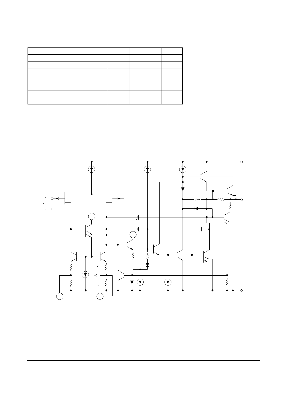
Inputs
–
+
J1 J2
Q1
V
CC
Q6
R1
240
18
D2
R
SC
Q7
C
M
Q4
Q3
Q2
Q8
Q9
500
Q10
R6
RM
Q11
D4
R3
1.0 k
Q5
C
C
C
F
20
pF
D3
V
EE
200
µ
A
Output
Null Adjust
(MC34080, 081)*
50 µA 850 µA
5.0
pF
3.0
pF
100
µ
A 300 µA
50 µA
500
Ω
R4
1.0 k
D1
R7
66 k
700
R2
+
+
1 5
Representative Schematic Diagram
(Each Amplifier)
Page 3
MC34080 thru MC34085
3
MOTOROLA ANALOG IC DEVICE DATA
DC ELECTRICAL CHARACTERISTICS (V
CC
= +15 V , VEE = – 15 V, TA = T
low
to T
high
[Note 3], unless otherwise noted.)
Characteristics Symbol Min Typ Max Unit
Input Offset Voltage (Note 4)
Single
TA = +25°C
TA = 0° to +70°C (MC34080B, MC34081B)
Dual
TA = +25°C
TA = 0° to +70°C (MC34082, MC34083)
Quad
TA = +25°C
TA = 0° to +70°C (MC34084, MC34085)
V
IO
—
—
—
—
—
—
0.5
—
1.0
—
6.0
—
2.0
4.0
3.0
5.0
12
14
mV
Average Temperature Coefficient of Of fset Voltage ∆VIO/∆T — 10 — µV/°C
Input Bias Current (VCM = 0 Note 5)
TA = +25°C
TA = 0° to +70°C
I
IB
——0.06
—
0.2
4.0
nA
Input Offset Current (VCM = 0 Note 5)
TA = +25°C
TA = 0° to +70°C
I
IO
——0.02—0.1
2.0
nA
Large Signal Voltage Gain (VO = ±10 V, RL = 2.0 k)
TA = +25°C
TA = T
low
to T
high
A
VOL
25
15
80
—
—
—
V/mV
Output Voltage Swing
RL = 2.0 k, TA = +25°C
RL = 10 k, TA = +25°C
RL = 10 k, TA = T
low to Thigh
V
OH
13.2
13.4
13.4
13.7
13.9
—
—
—
—
V
RL = 2.0 k, TA = +25°C
RL = 10 k, TA = +25°C
RL = 10 k, TA = T
low to Thigh
V
OL
—
—
—
–14.1
–14.7
—
–13.5
–14.1
–14.0
Output Short Circuit Current (TA = +25°C)
Input Overdrive = 1.0 V , Output to Ground
Source
Sink
I
SC
20
20
31
28
—
—
mA
Input Common Mode Voltage Range
TA = +25°C
V
ICR
(VEE +4.0) to
(VCC – 2.0)
V
Common Mode Rejection Ratio (RS ≤ 10 k, TA = +25°C) CMRR 70 90 — dB
Power Supply Rejection Ratio (RS = 100 Ω, TA = 25°C) PSRR 70 86 — dB
Power Supply Current
Single
TA = +25°C
TA = T
low
to T
high
Dual
TA = +25°C
TA = T
low
to T
high
Quad
TA = +25°C
TA = T
low
to T
high
I
D
—
—
—
—
—
—
2.5
—
4.9
—
9.7
—
3.4
4.2
6.0
7.5
11
13
mA
NOTES: (continued)
3.T
low
=0°C for MC34080B T
high
= +70°C for MC34080B
0°C for MC34081B +70°C for MC34081B
0°C for MC34084 +70°C for MC34084
0°C for MC34085 +70°C for MC34085
4.See application information for typical changes in input offset voltage due to solderability and temperature cycling.
5.Limits at TA = +25°C are guaranteed by high temperature (T
high
) testing.
Page 4
MC34080 thru MC34085
4
MOTOROLA ANALOG IC DEVICE DATA
AC ELECTRICAL CHARACTERISTICS
(VCC = +15 V , VEE = – 15 V, TA = +25°C, unless otherwise noted.)
Characteristics Symbol Min Typ Max Unit
Slew Rate (Vin = –10 V to +10 V, RL = 2.0 kΩ, CL = 100 pF)
Compensated AV = +1.0
AV = –1.0
Decompensated AV = +2.0
AV = –1.0
SR
20
—
35
—
25
30
50
50
—
—
—
—
V/µs
Settling Time (10 V Step, AV = –1.0)
To 0.10% (±1/2 LSB of 9–Bits)
To 0.01% (±1/2 LSB of 12–Bits)
t
s
——0.72
1.6
—
—
µs
Gain Bandwidth Product (f = 200 kHz)
Compensated
Decompensated
GBW
6.0128.0
16
—
—
MHz
Power Bandwidth (RL = 2.0 k, VO = 20 Vpp, THD = 5.0%)
Compensated AV = +1.0
Decompensated AV = – 1.0
BWp
——400
800——
kHz
Phase Margin (Compensated)
RL = 2.0 k
RL = 2.0 k, CL = 100 pF
φ
m
—
—
55
39
—
—
De-
grees
Gain Margin (Compensated)
RL = 2.0 k
RL = 2.0 k, CL = 100 pF
A
m
——7.6
4.5
—
—
dB
Equivalent Input Noise Voltage
RS = 100 Ω, f = 1.0 kHz
e
n
— 30 —
nV/ Hz√
Equivalent Input Noise Current (f = 1.0 kHz) I
n
— 0.01 —
pA/ Hz√
Input Capacitance C
i
— 5.0 — pF
Input Resistance r
i
— 10
12
— Ω
Total Harmonic Distortion
AV = +10, RL = 2.0 k, 2.0 ≤ VO ≤ 20 Vpp, f = 10 kHz
THD — 0.05 — %
Channel Separation (f = 10 kHz) — — 120 — dB
Open Loop Output Impedance (f = 1.0 MHz) Z
o
— 35 — Ω
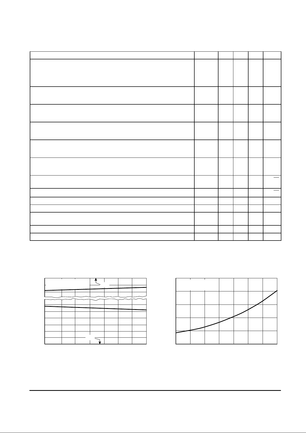
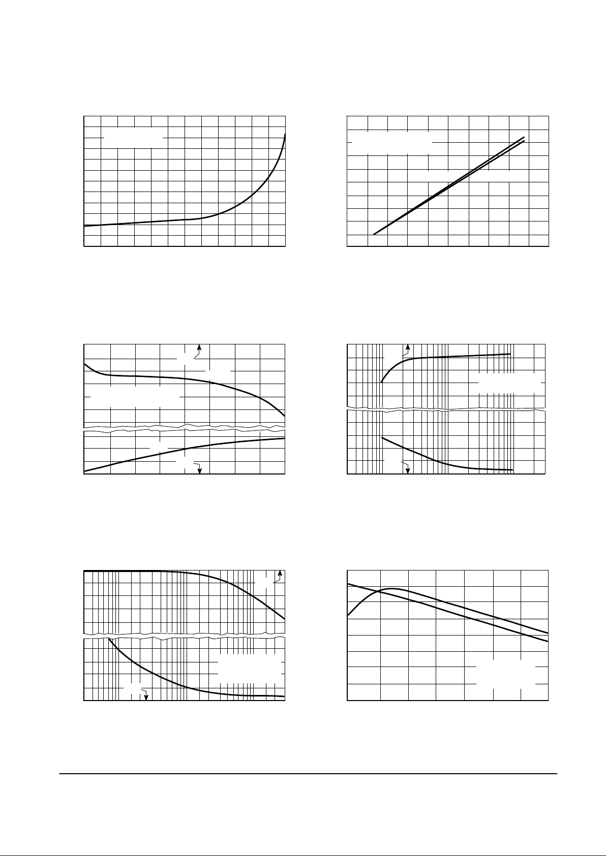
Figure 1. Input Common Mode Voltage Range
versus Temperature
Figure 2. Input Bias Current
versus Temperature
TA, AMBIENT TEMPERATURE (°C)
–55 –25 0 25 50 75 100 125
V , INPUT COMMON MODE VOLTAGE RANGE (V)
ICR
V
EE
VCC/VEE =
±
3.0 V to ±22 V
∆
VIO = 5.0 mA
V
CC
TA, AMBIENT TEMPERATURE (°C)
–55 –25 0 25 50 75 100 125
I , INPUT BIAS CURRENT (pA)
IB
VCC/VEE = ±15 V
VCM = 0 V
0
–1.0
3.0
2.0
1.0
0
100 k
10 k
1.0 k
100
10
1.0
Page 5
MC34080 thru MC34085
5
MOTOROLA ANALOG IC DEVICE DATA
Sink
Source
VCC/VEE = ±15 V
RL
≤
0.1
Ω
∆
Vin = 1.0 V
VCC/VEE = +15 V
RL to V
CC
TA = 25°C
V
EE
V
CC
VCC/VEE = ±15 V
TA = 25
°
C
V
CC
V
EE
VCC/VEE = +15 V to +22 V
TA = 25
°
C
V
CC
V
EE
Sink
Source
V
O
, OUTPUT VOL TAGE SWING (V
pp
)
Figure 3. Input Bias Current versus
Input Common Mode Voltage
Figure 4. Output Voltage Swing
versus Supply Voltage
Figure 5. Output Saturation versus
Load Current
Figure 6. Output Saturation vesus
Load Resistance to Ground
Figure 7. Output Saturation versus
Load Resistance to V
CC
Figure 8. Output Short Circuit Current
versus Temperature
I
IB
–12 –8.0 –4.0 0 4.0 8.0 12
VIC, INPUT COMMON MODE VOLTAGE (V)
VCC/VEE =±15 V
TA = 25
°
C
0
±
5.0
±
10
±
15
±
20
±
25
VCC |VEE|, SUPPLY VOLT AGE (V)
RL = 10 k
RL Connected to Ground
TA = 25
°
C
RL = 2.0 k
0 4.0 8.0 12 16
IL, LOAD CURRENT (
±
mA)
V
sat
300 3.0 k 30 k 300 k
RL, LOAD RESISTANCE T O GROUND (
Ω
)
300 3.0 k 30 k 300 k
RL, LOAD RESISTANCE T O VCC (
Ω
)
–55 –25 0 25 50 75 100 125
I , OUTPUT SHORT CIRCUIT CURRENT (mA)
SC
TA, AMBIENT TEMPERATURE (°C)
, INPUT BIAS CURRENT (pA), OUTPUT SA TURATION VOLTAGE (V)
V
sat
, OUTPUT SA TURATION VOLTAGE (V)
V
sat
, OUTPUT SA TURATION VOLTAGE (V)
140
120
100
80
60
40
20
50
40
30
20
10
0
0
–1.0
–2.0
–3.0
1.0
0
0
–2.0
–4.0
2.0
1.0
0
0
–0.4
–0.8
2.0
1.0
0
40
30
10
0
20
Page 6

MC34080 thru MC34085
6
MOTOROLA ANALOG IC DEVICE DATA
VCC/VEE = ±15 V
VCM = 0
VO = 0
∆
IO = ±0.5 mA
TA = 25
°
C
Decompensated
Units Only
AV = 1000
AV = 100
AV = 2.0
AV = 10
V
O
, OUTPUT VOL TAGE SWING (V
pp
)
Figure 9. Output Impedance versus Frequency Figure 10. Output Impedance versus Frequency
Figure 11. Output Voltage Swing
versus Frequency
Figure 12. Output Distortion versus Frequency
Figure 13. Open Loop Voltage Gain
versus Temperature
Z , OUTPUT IMPEDANCE ( )
O
Ω
f, FREQUENCY (Hz)
1.0 k 10 k 100 k 1.0 M 10 M
AV = 10
VCC/VEE = ±15 V
VCM = 0
VO = 0
∆
IO = ±0.5 mA
TA = 25
°
C
Compensated
Units Only
AV = 1000
AV = 100
AV = 1000
AV = 1.0
Z , OUTPUT IMPEDANCE ( )
O
Ω
f, FREQUENCY (Hz)
1.0 k 10 k 100 k 1.0 M 10 M
10 k 100 k 1.0 M 10 M
f, FREQUENCY (Hz)
10 100 1.0 k 10 k 100 k
AV = 1.0*
THD, OUTPUT DISTORTION (%)
f, FREQUENCY (Hz)
AV = 10
VCC/VEE = ±15 V
VO = 2.0 V
pp
RL = 2.0 k
TA = 25
°
C
*Compensated
Units Only
–55 –25 0 25 75 10050 125
VOL
A , OPEN LOOP VOL TAGE GAIN
(dB NORMALIZED)
TA, AMBIENT TEMPERATURE (°C)
VCC/VEE = ±15 V
VO = –10 V to +10 V
RL = 10 k
f
≤
10 Hz
80
60
40
20
0
80
60
40
20
0
28
24
20
16
12
8.0
4.0
0
0.5
0.4
0.3
0.2
0.1
0
1.08
1.04
1.00
0.96
0.92
VCC/VEE = ±15 V
RL = 2.0 k
THD = 1.0%
TA = 25
°
C
Decompensated
Units AV = –1.0
Compensated
Units AV = +1.0
AV = 1000
AV = 100
Page 7

MC34080 thru MC34085
7
MOTOROLA ANALOG IC DEVICE DATA
1 — Gain, RL = 2.0 k
2 — Gain, RL = 2.0 k, CL = 100 pF
3 — Phase, RL = 2.0 k
4 — Phase, RL = 2.0 k, CL = 100 pF
Decompensated Units Only
VCC/VEE = ±15 V
VO = 0 V
TA = 25
°
C
Phase
Margin
= 43
°
Gain
Margin
= 5.5 dB
Figure 14. Open Loop Voltage Gain and
Phase versus Frequency
Figure 15. Open Loop Voltage Gain and
Phase versus Frequency
Figure 16. Open Loop Voltage Gain and
Phase versus Frequency
Figure 17. Normalized Gain Bandwidth
Product versus Temperature
Figure 18. Percent Overshoot versus
Load Capacitance
Figure 19. Phase Margin versus
Load Capacitance
1.0 10 100 1.0 k 100 k 1.0 M 10 M 100 M10 k
f, FREQUENCY (Hz)
VOL
A , OPEN LOOP VOLTAGE GAIN (dB)
Phase Gain
, EXCESS PHASE (DEGREES)
φ
Solid Line Curves — Compensated Units
Dashed Line Curves — Decompensated Units
VCC/VEE =
±
15 V
VO = 0 V
RL = 2.0 k
TA = 25
°
C
1.0 2.0 3.0 5.0 7.0 10 20 30 50
f, FREQUENCY (Hz)
1
2
3
4
, EXCESS PHASE (DEGREES)
φ
1 — Gain, RL = 2.0 k
2 — Gain, RL = 2.0 k, CL = 100 pF
3 — Phase, RL = 2.0 k
4 — Phase, RL = 2.0 k, CL = 100 pF
Compensated Units Only
VCC/VEE = ±15 V
VO = 0 V
TA = 25
°
C
Phase
Margin
= 54
°
Gain
Margin
= 7.6 dB
1.0 2.0 3.0 5.0 7.0 10 20 30 50
f, FREQUENCY (Hz)
–55 –25 0 25 50 75 100 125
TA, AMBIENT TEMPERATURE (
°
C)
GBW, GAIN BANDWIDTH PRODUCT (NORMALIZED)
VCC/VEE = ±15 V
RL = 2.0 k
10 100 1.0k
CL, LOAD CAPACITANCE (pF)
PERCENT OVERSHOOT
VCC/VEE = ±15 V
RL = 2.0 k
∆
VO = 100 mV
pp
VO = –10 V to +10 V
TA = 25
°
C
Decompensated
Units AV = +2.0
Compensated
Units AV = +1.0
10 100 1.0k
CL, LOAD CAPACITANCE (pF)
VCC/VEE = ±15 V
RL = 2.0 k to
R
∆
VO = 100 mV
pp
VO = –10 V to +10 V
TA = 25°C
Decompensated
Units AV = +2.0
Compensated
Units AV = +1.0
M
φ
, PHASE MARGIN (DEGREES)
, EXCESS PHASE (DEGREES)
φ
VOL
A , OPEN LOOP VOLTAGE GAIN (dB)
VOL
A , OPEN LOOP VOLTAGE GAIN (dB)
100
80
60
40
20
0
20
10
0
–10
–20
–30
–40
20
10
0
–10
–20
–30
–40
1.20
1.10
1.00
0.90
0.80
100
80
60
40
20
0
70
60
50
40
30
20
10
0
100
120
140
160
180
200
100
120
140
160
180
200
0
45
90
135
180
Page 8

MC34080 thru MC34085
8
MOTOROLA ANALOG IC DEVICE DATA
Solid Line Curves–Compensated Units A
V
= +1.0
Dashed Line Curves–Decompensated Units A
V
= +2.0
VCC/VEE = ±15 V
RL = 2.0 k to
∞
∆
VO = 100 mV
pp
VO = –10 V to +10 V
CL = 10 pF
CL = 200 pF
CL = 360 pF
CL = 100 pF
Figure 20. Gain Margin versus Load Capacitance Figure 21. Phase Margin versus Temperature
Figure 22. Gain Margin versus Temperature
Figure 23. Normalized Slew Rate
versus Temperature
10 100 10 k
CL, LOAD CAPACITANCE (pF)
A , GAIN MARGIN (dB)
m
VCC/VEE = ±15 V
RL = 2.0 k to
∞
∆
VO = 100 mV
pp
VO = –10 V to +10 V
TA = 25°C
Compensated
Units AV = +1.0
Decompensated
Units AV = +2.0
–55 –25 0 25 50 75 100 125
m
TA, AMBIENT TEMPERATURE (°C)
φ
, PHASE MARGIN (DEGREES)
CL = 10 pF
CL = 360 pF
CL = 200 pF
Solid Line Curves–Compensated Units A
V
= +1.0
Dashed Line Curves–Decompensated Units A
V
= +2.0
VCC/VEE =
±
15 V
RL = 2.0 k to
∞
∆
VO = 100 mV
pp
VO = –10 V to +10 V
CL = 100 pF
–55 –25 0 25 50 75 100 125
TA, AMBIENT TEMPERATURE (
°
C)
SR, SLEW RATE (NORMALIZED)
–55 –25 0 25 50 75 100 125
TA, AMBIENT TEMPERATURE (
°
C)
VCC/VEE = ±15 V
AV = +1.0 for Compensated Units
AV = –1.0 for Decompensated Units
RL = 2.0 k
CL = 100 pF
VO = –10 V to +10 V
A , GAIN MARGIN (dB)
m
10
8.0
6.0
4.0
2.0
0
60
50
40
30
20
10
0
10
8.0
6.0
4.0
2.0
0
1.40
1.20
1.00
0.80
0.60
Page 9

MC34080 thru MC34085
9
MOTOROLA ANALOG IC DEVICE DATA
MC34084 Transient Response
AV = +1.0, RL = 2.0 k, VCC/VEE = ±15 V, TA = 25°C
Figure 24. Small Signal Figure 25. Large Signal
MC34085 Transient Response
AV = +2.0, RL = 2.0 k, VCC/VEE = ±15 V, TA = 25°C
Figure 26. Small Signal Figure 27. Large Signal
0
0
0 0
0.2 µs/Div 0.5 µs/Div
0.2
µ
s/Div 0.5 µs/Div
50 mV/Div
5.0 mV/Div
50 mV/Div
5.0 mV/Div
CL = 10 pF
CL = 10 pF
CL = 100 pF
CL = 100 pF
Page 10

MC34080 thru MC34085
10
MOTOROLA ANALOG IC DEVICE DATA
TA = 125°C
TA = 25°C
TA = –55
°
C
Supply Current
Normalized to
VCC/VEE =
±
15 V, TA = 25°C
RL =
∞
VO = 0
TA = 25°C
Figure 28. Common Mode Rejection Ratio
versus Frequency
Figure 29. Power Supply Rejection Ratio
versus Frequency
Figure 30. Power Supply Rejection Ratio
versus Temperature
Figure 31. Normalized Supply Current
versus Supply Voltage
Figure 32. Channel Separation versus Frequency Figure 33. Spectral Noise Density
0.1 1.0 10 100 1.0 k 10 k 100 k 1.0 M 10 M
CMRR, COMMON MODE REJECTION RATIO (dB)
f, FREQUENCY (Hz)
VCC/VEE = ±15 V
∆
VS = 3.0 V
VO = 0 V
TA = –55°C
TA = 125°C
0.1 1.0 10 100 1.0 k 10 k 100 k 1.0 M 10 M
f, FREQUENCY (Hz)
PSSR, POWER SUPPLY REJECTION RATIO (dB)
VCC/VEE = ±15 V
∆
VS = 3.0 V
VO = 0 V
TA = 25
°
C
Positive
Supply
Negative
Supply
Compensated Units AV = +1.0
Decompensated Units AV = +2.0
VCC/VEE = ±15 V
∆
VS = 3.0 V
VO = 0 V
f
≤
10 Hz
Positive
Supply
Negative
Supply
–55 –25 0 25 50 75 100 125
PSSR, POWER SUPPLY REJECTION RATION (dB)
TA, AMBIENT TEMPERATURE (°C)
0
±
5.0
±
10
±
15
±
20
±
25
I , SUPPLY CURRENT (NORMALIZED)
CC
VS, SUPPLY VOLT AGE (V)
10 k 100 k 1.0 M 10 M
CHANNEL SEPERATION (dB)
f, FREQUENCY (Hz)
VCC/VEE = ±15 V
TA = 25
°
C
10 k 100 k10 100 1.0 k
e , INPUT NOISE VOLTAGE (
n
f, FREQUENCY (Hz)
nV/ Hz )
√
VCC/VEE = ±15 V
VCM = 0
TA = 25
°
C
Compensated Units AV = +1.0
Decompensated Units AV = +2.0
100
80
60
40
20
0
120
100
80
60
40
20
0
110
100
90
80
70
1.20
1.10
1.00
0.90
0.80
0.70
120
100
80
60
40
20
0
100
80
60
40
20
0
VCC ± ∆V
CC
+
V
O
–
VCC ± ∆V
CC
VEE
± ∆
V
EE
+
V
O
–
VCC ± ∆V
CC
VEE
± ∆
V
EE
+
V
O
–
VEE ± ∆V
EE
Page 11

MC34080 thru MC34085
11
MOTOROLA ANALOG IC DEVICE DATA
APPLICATIONS INFORMATION
The bandwidth and slew rate of the MC34080 series is
nearly double that of currently available general purpose
JFET op–amps. This improvement in AC performance is due
to the P–channel JFET differential input stage driving a
compensated miller integration amplifier in conjunction with
an all NPN output stage.
The all NPN output stage offers unique advantages over
the more conventional NPN/PNP transistor Class AB output
stage. With a 10 k load resistance, the op amp can typically
swing within 1.0 V of the positive rail (VCC), and within 0.3 V
of the negative rail (VEE), providing a 28.7 p–p swing from
±15 V supplies. This large output swing becomes most
noticeable at lower supply voltages. If the load resistance is
referenced to VCC instead of ground, the maximum possible
output swing can be achieved for a given supply voltage. For
light load currents, the load resistance will pull the output to
VCC during the positive swing and the NPN output transistor
will pull the output very near VEE during the negative swing.
The load resistance value should be much less than that of
the feedback resistance to maximize pull–up capability.
The all NPN transistor output stage is also inherently
fast, contributing to the operation amplifier’s high
gain–bandwidth product and fast settling time. The
associated high frequency output impedance is 50 Ω (typical)
at 8.0 MHz. This allows driving capacitive loads from 0 pF to
300 pF without oscillations over the military temperature
range, and over the full range of output swing. The 55°C
phase margin and 7.6 dB gain margin as well as the general
gain and phase characteristics are virtually independent of
the sink/source output swing conditions. The high frequency
characteristics of the MC34080 series is especially useful for
active filter applications.
The common mode input range is from 2.0 V below the
positive rail (VCC) to 4.0 V above the negative rail (VEE). The
amplifier remains active if the inputs are biased at the positive
rail. This may be useful for some applications in that single
supply operation is possible with a single negative supply.
However, a degradation of offset voltage and voltage gain
may result.
Phase reversal does not occur if either the inverting or
noninverting input (or both) exceeds the positive common
mode limit. If either input (or both) exceeds the negative
common mode limit, the output will be in the high state. The
input stage also allows a differential up to ±44 V , provided the
maximum input voltage range is not exceeded. The supply
voltage operating range is from ±5.0 V to ±22 V.
For optimum frequency performance and stability, careful
component placement and printed circuit board layout should
be exercised. For example, long unshielded input or output
leads may result in unwanted input–output coupling. In order
to reduce the input capacitance, resistors connected to the
input pins should be physically close to these pins. This not
only minimizes the input pole for optimum frequency
response, but also minimizes extraneous “pickup” at
this node.
Supply decoupling with adequate capacitance close to the
supply pin is also important, particularly over temperature,
since many types of decoupling capacitors exhibit large
impedance changes over temperature.
Primarily due to the JFET inputs of the op amp, the input
offset voltage may change due to temperature cycling and
board soldering. After 20 temperature cycles (– 55° to
165°C), the typical standard deviation for input offset voltage
is 559 µV in the plastic packages. With respect to board
soldering (260°C, 10 seconds), the typical standard deviation
for input offset voltage is 525 µV in the plastic package.
Socketed devices should be used over a minimal
temperature range for optimum input offset voltage
performance.
3
2
4
1
5
6
7
+
–
5.0 k
V
CC
V
EE
Figure 34. Offset Nulling Circuit
Page 12

MC34080 thru MC34085
12
MOTOROLA ANALOG IC DEVICE DATA
P SUFFIX
PLASTIC PACKAGE
CASE 626–05
ISSUE K
D SUFFIX
PLASTIC PACKAGE
CASE 751–05
(SO–8)
ISSUE R
OUTLINE DIMENSIONS
NOTES:
1. DIMENSION L TO CENTER OF LEAD WHEN
FORMED PARALLEL.
2. PACKAGE CONTOUR OPTIONAL (ROUND OR
SQUARE CORNERS).
3. DIMENSIONING AND TOLERANCING PER ANSI
Y14.5M, 1982.
14
58
F
NOTE 2
–A–
–B–
–T–
SEATING
PLANE
H
J
G
D
K
N
C
L
M
M
A
M
0.13 (0.005) B
M
T
DIM MIN MAX MIN MAX
INCHESMILLIMETERS
A 9.40 10.16 0.370 0.400
B 6.10 6.60 0.240 0.260
C 3.94 4.45 0.155 0.175
D 0.38 0.51 0.015 0.020
F 1.02 1.78 0.040 0.070
G 2.54 BSC 0.100 BSC
H 0.76 1.27 0.030 0.050
J 0.20 0.30 0.008 0.012
K 2.92 3.43 0.115 0.135
L 7.62 BSC 0.300 BSC
M ––– 10 ––– 10
N 0.76 1.01 0.030 0.040
__
SEATING
PLANE
1
4
58
A0.25MCB
SS
0.25MB
M
h
q
C
X 45
_
L
DIM MIN MAX
MILLIMETERS
A 1.35 1.75
A1 0.10 0.25
B 0.35 0.49
C 0.18 0.25
D 4.80 5.00
E
1.27 BSCe
3.80 4.00
H 5.80 6.20
h
0 7
L 0.40 1.25
q
0.25 0.50
__
NOTES:
1. DIMENSIONING AND TOLERANCING PER ASME
Y14.5M, 1994.
2. DIMENSIONS ARE IN MILLIMETERS.
3. DIMENSION D AND E DO NOT INCLUDE MOLD
PROTRUSION.
4. MAXIMUM MOLD PROTRUSION 0.15 PER SIDE.
5. DIMENSION B DOES NOT INCLUDE MOLD
PROTRUSION. ALLOWABLE DAMBAR
PROTRUSION SHALL BE 0.127 TOTAL IN EXCESS
OF THE B DIMENSION AT MAXIMUM MATERIAL
CONDITION.
D
E
H
A
B
e
B
A1
C
A
0.10
Page 13

MC34080 thru MC34085
13
MOTOROLA ANALOG IC DEVICE DATA
P SUFFIX
PLASTIC PACKAGE
CASE 646–06
ISSUE L
OUTLINE DIMENSIONS
NOTES:
1. LEADS WITHIN 0.13 (0.005) RADIUS OF TRUE
POSITION AT SEATING PLANE AT MAXIMUM
MATERIAL CONDITION.
2. DIMENSION L TO CENTER OF LEADS WHEN
FORMED PARALLEL.
3. DIMENSION B DOES NOT INCLUDE MOLD
FLASH.
4. ROUNDED CORNERS OPTIONAL.
17
14 8
B
A
F
HG D
K
C
N
L
J
M
SEATING
PLANE
DIM MIN MAX MIN MAX
MILLIMETERSINCHES
A 0.715 0.770 18.16 19.56
B 0.240 0.260 6.10 6.60
C 0.145 0.185 3.69 4.69
D 0.015 0.021 0.38 0.53
F 0.040 0.070 1.02 1.78
G 0.100 BSC 2.54 BSC
H 0.052 0.095 1.32 2.41
J 0.008 0.015 0.20 0.38
K 0.115 0.135 2.92 3.43
L 0.300 BSC 7.62 BSC
M 0 10 0 10
N 0.015 0.039 0.39 1.01
____
DW SUFFIX
PLASTIC PACKAGE
CASE 751G–02
(SO–16L)
ISSUE A
DIM MIN MAX MIN MAX
INCHESMILLIMETERS
A 10.15 10.45 0.400 0.411
B 7.40 7.60 0.292 0.299
C 2.35 2.65 0.093 0.104
D 0.35 0.49 0.014 0.019
F 0.50 0.90 0.020 0.035
G 1.27 BSC 0.050 BSC
J 0.25 0.32 0.010 0.012
K 0.10 0.25 0.004 0.009
M 0 7 0 7
P 10.05 10.55 0.395 0.415
R 0.25 0.75 0.010 0.029
M
B
M
0.010 (0.25)
NOTES:
1. DIMENSIONING AND TOLERANCING PER ANSI
Y14.5M, 1982.
2. CONTROLLING DIMENSION: MILLIMETER.
3. DIMENSIONS A AND B DO NOT INCLUDE MOLD
PROTRUSION.
4. MAXIMUM MOLD PROTRUSION 0.15 (0.006) PER
SIDE.
5. DIMENSION D DOES NOT INCLUDE DAMBAR
PROTRUSION. ALLOWABLE DAMBAR
PROTRUSION SHALL BE 0.13 (0.005) TOTAL IN
EXCESS OF D DIMENSION AT MAXIMUM
MATERIAL CONDITION.
–A–
–B– P8X
G14X
D16X
SEATING
PLANE
–T–
S
A
M
0.010 (0.25) B
S
T
16 9
81
F
J
R
X 45
_
____
M
C
K
Page 14

MC34080 thru MC34085
14
MOTOROLA ANALOG IC DEVICE DATA
NOTES
Page 15

MC34080 thru MC34085
15
MOTOROLA ANALOG IC DEVICE DATA
NOTES
Page 16

MC34080 thru MC34085
16
MOTOROLA ANALOG IC DEVICE DATA
Motorola reserves the right to make changes without further notice to any products herein. Motorola makes no warranty , representation or guarantee regarding
the suitability of its products for any particular purpose, nor does Motorola assume any liability arising out of the application or use of any product or circuit, and
specifically disclaims any and all liability, including without limitation consequential or incidental damages. “T ypical” parameters which may be provided in Motorola
data sheets and/or specifications can and do vary in different applications and actual performance may vary over time. All operating parameters, including “Typicals”
must be validated for each customer application by customer’s technical experts. Motorola does not convey any license under its patent rights nor the rights of
others. Motorola products are not designed, intended, or authorized for use as components in systems intended for surgical implant into the body, or other
applications intended to support or sustain life, or for any other application in which the failure of the Motorola product could create a situation where personal injury
or death may occur. Should Buyer purchase or use Motorola products for any such unintended or unauthorized application, Buyer shall indemnify and hold Motorola
and its officers, employees, subsidiaries, affiliates, and distributors harmless against all claims, costs, damages, and expenses, and reasonable attorney fees
arising out of, directly or indirectly, any claim of personal injury or death associated with such unintended or unauthorized use, even if such claim alleges that
Motorola was negligent regarding the design or manufacture of the part. Motorola and are registered trademarks of Motorola, Inc. Motorola, Inc. is an Equal
Opportunity/Affirmative Action Employer.
How to reach us:
USA/EUROPE / Locations Not Listed: Motorola Literature Distribution; JAPAN: Nippon Motorola Ltd.; Tatsumi–SPD–JLDC, 6F Seibu–Butsuryu–Center,
P.O. Box 20912; Phoenix, Arizona 85036. 1–800–441–2447 or 602–303–5454 3–14–2 Tatsumi Koto–Ku, Tokyo 135, Japan. 03–81–3521–8315
MFAX: RMF AX0@email.sps.mot.com – TOUCHT ONE 602–244–6609 ASIA/PACIFIC: Motorola Semiconductors H.K. Ltd.; 8B Tai Ping Industrial Park,
INTERNET: http://Design–NET.com 51 Ting Ko k Road, Tai Po, N.T., Hong Kong. 852–26629298
MC34080/D
*MC34080/D*
◊
 Loading...