

Page 1
MC34063A, MC33063A,
SC34063A, SC33063A,
NCV33063A
1.5 A, Step-Up/Down/
Inverting Switching
Regulators
www.onsemi.com
The MC34063A Series is a monolithic control circuit containing the
primary functions required for DC−to−DC converters. These devices
consist of an internal temperature compensated reference, comparator,
controlled duty cycle oscillator with an active current limit circuit,
driver and high current output switch. This series was specifically
designed to be incorporated in Step−Down and Step−Up and
Voltage−Inverting applications with a minimum number of external
components. Refer to Application Notes AN920A/D and AN954/D
for additional design information.
Features
• Operation from 3.0 V to 40 V Input
• Low Standby Current
• Current Limiting
• Output Switch Current to 1.5 A
• Output Voltage Adjustable
• Frequency Operation to 100 kHz
• Precision 2% Reference
• NCV Prefix for Automotive and Other Applications Requiring
Unique Site and Control Change Requirements; AEC−Q100
Qualified and PPAP Capable
• These Devices are Pb−Free, Halogen Free/BFR Free and are RoHS
Compliant
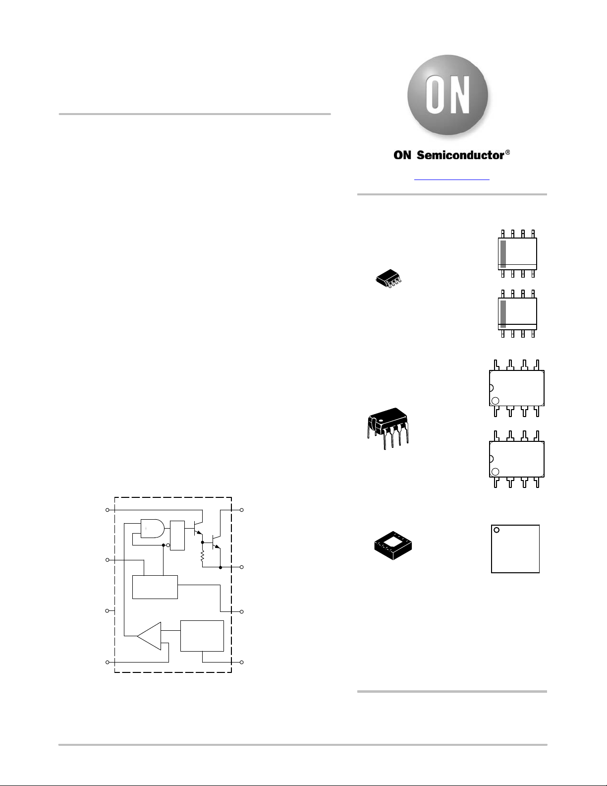
MARKING
DIAGRAMS
8
3x063
ALYWA
8
1
8
1
SOIC−8
D SUFFIX
CASE 751
PDIP−8
P, P1 SUFFIX
CASE 626
G
1
8
3x063V
ALYWA
G
1
8
3x063AP1
AWL
YYWWG
1
8
33063AVP
AWL
YYWWG
1
8
Drive
Collector
Q2
Q1
100
1.25 V
Reference
Regulator
Sense
V
Comparator
Inverting
Input
SQ
7
I
pk
Oscillator
6
CC
This device contains 79 active transistors.
R
I
pk
C
Comparator
+
-
(Bottom View)
T
Figure 1. Representative Schematic Diagram
© Semiconductor Components Industries, LLC, 2016
December, 2016 − Rev. 24
1
Switch
Collector
2
Switch
Emitter
3
Timing
Capacitor
45
GND
DFN8
CASE 488AF
1
x = 3 or 4
A = Assembly Location
L, WL = Wafer Lot
Y, YY = Year
W, WW = Work Week
G or G = Pb−Free Package
33063
ALYWA
G
ORDERING INFORMATION
See detailed ordering and shipping information in the package
dimensions section on page 12 of this data sheet.
1 Publication Order Number:
MC34063A/D
Page 2

MC34063A, MC33063A, SC34063A, SC33063A, NCV33063A
Switch
Collector
Switch
Emitter
Timing
Capacitor
GND
1
2
3
45
(Top View)
8
7
6
Driver
Collector
I
Sense
pk
V
CC
Comparator
Inverting
Input
Switch Collector
Switch Emitter
Timing Capacitor
GND
EP Flag
(Top View)
Driver Collector
Sense
I
pk
V
CC
Comparator
Inverting Input
Figure 2. Pin Connections
MAXIMUM RATINGS
Rating Symbol Value Unit
Power Supply Voltage V
Comparator Input Voltage Range V
Switch Collector Voltage V
Switch Emitter Voltage (V
= 40 V) V
Pin 1
Switch Collector to Emitter Voltage V
Driver Collector Voltage V
Driver Collector Current (Note 1) I
Switch Current I
CC
IR
C(switch)
E(switch)
CE(switch)
C(driver)
C(driver)
SW
Power Dissipation and Thermal Characteristics
Plastic Package, P, P1 Suffix
TA = 25°C P
Thermal Resistance
D
R
q
JA
SOIC Package, D Suffix
TA = 25°C P
Thermal Resistance
Thermal Resistance
D
R
q
JA
R
q
JC
DFN Package
TA = 25°C P
Thermal Resistance
Operating Junction Temperature T
Operating Ambient Temperature Range T
D
R
q
JA
J
A
MC34063A, SC34063A 0 to +70
MC33063AV, NCV33063A −40 to +125
MC33063A, SC33063A −40 to +85
Storage Temperature Range T
stg
Stresses exceeding those listed in the Maximum Ratings table may damage the device. If any of these limits are exceeded, device functionality
should not be assumed, damage may occur and reliability may be affected.
1. Maximum package power dissipation limits must be observed.
2. This device series contains ESD protection and exceeds the following tests: Human Body Model 4000 V per MIL−STD−883, Method 3015.
Machine Model Method 400 V.
3. NCV prefix is for automotive and other applications requiring site and change control.
40 Vdc
−0.3 to +40 Vdc
40 Vdc
40 Vdc
40 Vdc
40 Vdc
100 mA
1.5 A
1.25 W
115 °C/W
625 mW
160 °C/W
45 °C/W
1.25 mW
80 °C/W
+150 °C
°C
−65 to +150 °C
www.onsemi.com
2
Page 3

MC34063A, MC33063A, SC34063A, SC33063A, NCV33063A
ELECTRICAL CHARACTERISTICS (V
Characteristics
= 5.0 V, TA = T
CC
low
to T
[Note 4], unless otherwise specified.)
high
Symbol Min Typ Max Unit
OSCILLATOR
Frequency (V
= 0 V, CT = 1.0 nF, TA = 25°C) f
Pin 5
Charge Current (VCC = 5.0 V to 40 V, TA = 25°C) I
Discharge Current (VCC = 5.0 V to 40 V, TA = 25°C) I
Discharge to Charge Current Ratio (Pin 7 to VCC, TA = 25°C) I
Current Limit Sense Voltage (I
chg
= I
, TA = 25°C) V
dischg
dischg/Ichg
ipk(sense)
osc
chg
dischg
24 33 42 kHz
24 35 42
140 220 260
mA
mA
5.2 6.5 7.5 −
250 300 350 mV
OUTPUT SWITCH (Note 5)
Saturation Voltage, Darlington Connection
= 1.0 A, Pins 1, 8 connected)
(I
SW
Saturation Voltage (Note 6)
(I
= 1.0 A, R
SW
= 82 W to VCC, Forced b ] 20)
Pin 8
DC Current Gain (ISW = 1.0 A, VCE = 5.0 V, TA = 25°C) h
Collector Off−State Current (VCE = 40 V) I
V
CE(sat)
V
CE(sat)
C(off)
FE
− 1.0 1.3 V
− 0.45 0.7 V
50 75 − −
− 0.01 100
mA
COMPARATOR
Threshold Voltage
= 25°C
T
A
= T
T
to T
A
low
high
Threshold Voltage Line Regulation (VCC = 3.0 V to 40 V)
MC33063, MC34063
MC33063V, NCV33063
Input Bias Current (Vin = 0 V) I
Reg
V
th
line
IB
1.225
1.21
−
−
1.25−1.275
1.29
1.4
1.4
5.0
6.0
− −20 −400 nA
V
mV
TOTAL DEVICE
Supply Current (VCC = 5.0 V to 40 V, CT = 1.0 nF, Pin 7 = VCC,
> Vth, Pin 2 = GND, remaining pins open)
V
Pin 5
I
CC
− − 4.0 mA
Product parametric performance is indicated in the Electrical Characteristics for the listed test conditions, unless otherwise noted. Product
performance may not be indicated by the Electrical Characteristics if operated under different conditions.
= 0°C for MC34063, SC34063; −40°C for MC33063, SC33063, MC33063V, NCV33063
4. T
low
= +70°C for MC34063, SC34063; +85°C for MC33063, SC33063; +125°C for MC33063V, NCV33063
T
high
5. Low duty cycle pulse techniques are used during test to maintain junction temperature as close to ambient temperature as possible.
6. If the output switch is driven into hard saturation (non−Darlington configuration) at low switch currents (≤ 300 mA) and high driver currents
(≥ 30 mA), it may take up to 2.0 ms for it to come out of saturation. This condition will shorten the off time at frequencies ≥ 30 kHz, and is
magnified at high temperatures. This condition does not occur with a Darlington configuration, since the output switch cannot saturate. If a
non−Darlington configuration is used, the following output drive condition is recommended:
Forced b of output switch :
ICoutput
ICdriver – 7.0 mA *
w 10
*The 100 W resistor in the emitter of the driver device requires about 7.0 mA before the output switch conducts.
www.onsemi.com
3
Page 4

MC34063A, MC33063A, SC34063A, SC33063A, NCV33063A
t
18
VCC = 5.0 V, Pin 7 = V
16
Pin 5 = GND, TA = 25°C
14
12
10
8
6
OFF TIME (ms)
4
2
0
0.0 0.5 1.0 1.5 2.0 2.5 3.0 3.5 4.0 4.5 5.0
Ct, TIMING CAPACITOR CAPACITANCE (nF)
CC
ON TIME (ms)
OFF TIME (ms)
FREQUENCY (kHz)
Figure 3. Oscillator Frequency
1.8
1.7
1.6
1.5
1.4
1.3
, SATURATION VOLTAGE (V)
1.2
1.1
CE(sat)
V
1.0
0 0.2 0.4 0.6 0.8 1.0 1.2 1.4 1.6
IE, EMITTER CURRENT (A)
VCC = 5.0 V
Pins 1, 7, 8 = V
Pins 3, 5 = GND
T
= 25°C
A
(See Note 7)
180
160
140
120
100
80
60
40
20
0
, OSCILLATOR VOLTAGE (V)
VCC = 5.0 V
OSC
Pin 7 = V
V
Pin 2 = GND
ON TIME (ms), FREQUENCY (kHz)
Pins 1, 5, 8 = Open
CC
CT = 1.0 nF
TA = 25°C
10 ms/DIV
200 mV/DIV
Figure 4. Timing Capacitor Waveform
1.1
1.0
0.9
0.8
0.7
0.6
VCC = 5.0 V
Pin 7 = V
0.5
0.4
, SATURATION VOLTAGE (V)
CC
0.3
0.2
CE(sat)
0.1
V
0
0 0.2 0.4 0.6 0.8 1.0 1.2 1.4 1.6
CC
Pins 2, 3, 5 = GND
TA = 25°C
(See Note 7)
IC, COLLECTOR CURRENT(A)
Darlington Connection
Forced b = 20
Figure 5. Emitter Follower Configuration Output
Saturation Voltage versus Emitter Current
Figure 6. Common Emitter Configuration Outpu
Switch Saturation Voltage versus
Collector Current
400
380
VCC = 5.0 V
360
I
= I
chg
340
320
300
280
260
, CURRENT LIMIT SENSE VOLTAGE (V)
240
220
200
IPK(sense)
-55 -25 0 25 50 75 100 125
V
dischg
TA, AMBIENT TEMPERATURE (°C)
Figure 7. Current Limit Sense Voltage
versus Temperature
7. Low duty cycle pulse techniques are used during test to maintain junction temperature as close to ambient temperature as possible.
3.6
3.2
2.8
2.4
2.0
1.6
1.2
, SUPPLY CURRENT (mA)
0.8
CC
I
0.4
0
0 5.0 10 15 20 25 30 35 40
VCC, SUPPLY VOLTAGE (V)
CT = 1.0 nF
Pin 7 = V
CC
Pin 2 = GND
Figure 8. Standby Supply Current versus
Supply Voltage
www.onsemi.com
4
Page 5

MC34063A, MC33063A, SC34063A, SC33063A, NCV33063A
170 mH
L
8
1
180
SQRQ2
Q1
V
12 V
7
I
R
sc
0.22
in
6
+
100
pk
V
CC
+
Comp.
-
OSC
C
T
1.25 V
Ref
Reg
5
2
3
C
4
1N5819
T
1500
pF
1.0 mH
R1 2.2 k
R2
47 k
+
330 C
28 V/175 mA
O
V
out
Test Conditions Results
Line Regulation Vin = 8.0 V to 16 V, IO = 175 mA 30 mV = ±0.05%
Load Regulation Vin = 12 V, IO = 75 mA to 175 mA 10 mV = ±0.017%
Output Ripple Vin = 12 V, IO = 175 mA 400 mVpp
Efficiency Vin = 12 V, IO = 175 mA 87.7%
Output Ripple With Optional Filter Vin = 12 V, IO = 175 mA 40 mVpp
+
100
Optional Filter
V
out
Figure 9. Step−Up Converter
www.onsemi.com
5
Page 6

MC34063A, MC33063A, SC34063A, SC33063A, NCV33063A
s
V
8
7
R
sc
V
in
6
1
2
out
8
7
R
sc
V
in
6
1
2
R
R ³ 0 for
constant V
in
Figure 10. External Current Boost Connections for IC Peak Greater than 1.5 A
9a. External NPN Switch 9b. External NPN Saturated Switch
(See Note 8)
8. If the output switch is driven into hard saturation (non−Darlington configuration) at low switch currents (≤ 300 mA) and high driver current
(≥ 30 mA), it may take up to 2.0 ms to come out of saturation. This condition will shorten the off time at frequencies ≥ 30 kHz, and is magnified
at high temperatures. This condition does not occur with a Darlington configuration, since the output switch cannot saturate. If a
non−Darlington configuration is used, the following output drive condition is recommended.
V
out
www.onsemi.com
6
Page 7

MC34063A, MC33063A, SC34063A, SC33063A, NCV33063A
V
Q1
1
2
1N5819
3
C
T
470
4
470 C
L
220 mH
pF
V
out
5.0 V/500 mA
1.0 mH
+
O
V
25 V
R
0.33
in
100
R1 1.2 k
8
SQ
Q2
R
7
I
sc
6
+
V
pk
CC
+
-
OSC
Comp.
C
T
1.25 V
Ref
Reg
5
R2
3.6 k
Test Conditions Results
Line Regulation Vin = 15 V to 25 V, IO = 500 mA 12 mV = ±0.12%
Load Regulation Vin = 25 V, IO = 50 mA to 500 mA 3.0 mV = ±0.03%
Output Ripple Vin = 25 V, IO = 500 mA 120 mVpp
Short Circuit Current
Vin = 25 V, RL = 0.1 W
1.1 A
Efficiency Vin = 25 V, IO = 500 mA 83.7%
Output Ripple With Optional Filter Vin = 25 V, IO = 500 mA 40 mVpp
+
100
Optional Filter
V
out
Figure 11. Step−Down Converter
8
1
8
7
R
sc
V
in
6
2
V
out
7
R
sc
V
in
6
1
2
Figure 12. External Current Boost Connections for IC Peak Greater than 1.5 A
11a. External NPN Switch 11b. External PNP Saturated Switch
www.onsemi.com
7
Page 8

MC34063A, MC33063A, SC34063A, SC33063A, NCV33063A
4.5 V to 6.0 V
V
Line Regulation Vin = 4.5 V to 6.0 V, IO = 100 mA 3.0 mV = ± 0.012%
Load Regulation Vin = 5.0 V, IO = 10 mA to 100 mA 0.022 V = ± 0.09%
Output Ripple Vin = 5.0 V, IO = 100 mA 500 mVpp
Short Circuit Current
Efficiency Vin = 5.0 V, IO = 100 mA 62.2%
Output Ripple With Optional Filter Vin = 5.0 V, IO = 100 mA 70 mVpp
R
sc
0.24
in
+
100
R2 8.2 k
8
1
SQRQ2
Q1
7
I
pk
6
V
CC
+
-
OSC
Comp.
C
T
1.25 V
Ref
Reg
5
R1
953
2
88 mH
L
3
+
1500
pF
1N5819
4
V
out
-12 V/100 mA
1000 mf
C
O
+
Test Conditions Results
Vin = 5.0 V, RL = 0.1 W
910 mA
1.0 mH
Optional Filter
V
out
100
+
Figure 13. Voltage Inverting Converter
8
7
V
in
6
1
8
2
V
out
3
7
V
in
6
1
V
out
2
+
3
+
4
4
Figure 14. External Current Boost Connections for IC Peak Greater than 1.5 A
13a. External NPN Switch 13b. External PNP Saturated Switch
www.onsemi.com
8
Page 9
MC34063A, MC33063A, SC34063A, SC33063A, NCV33063A
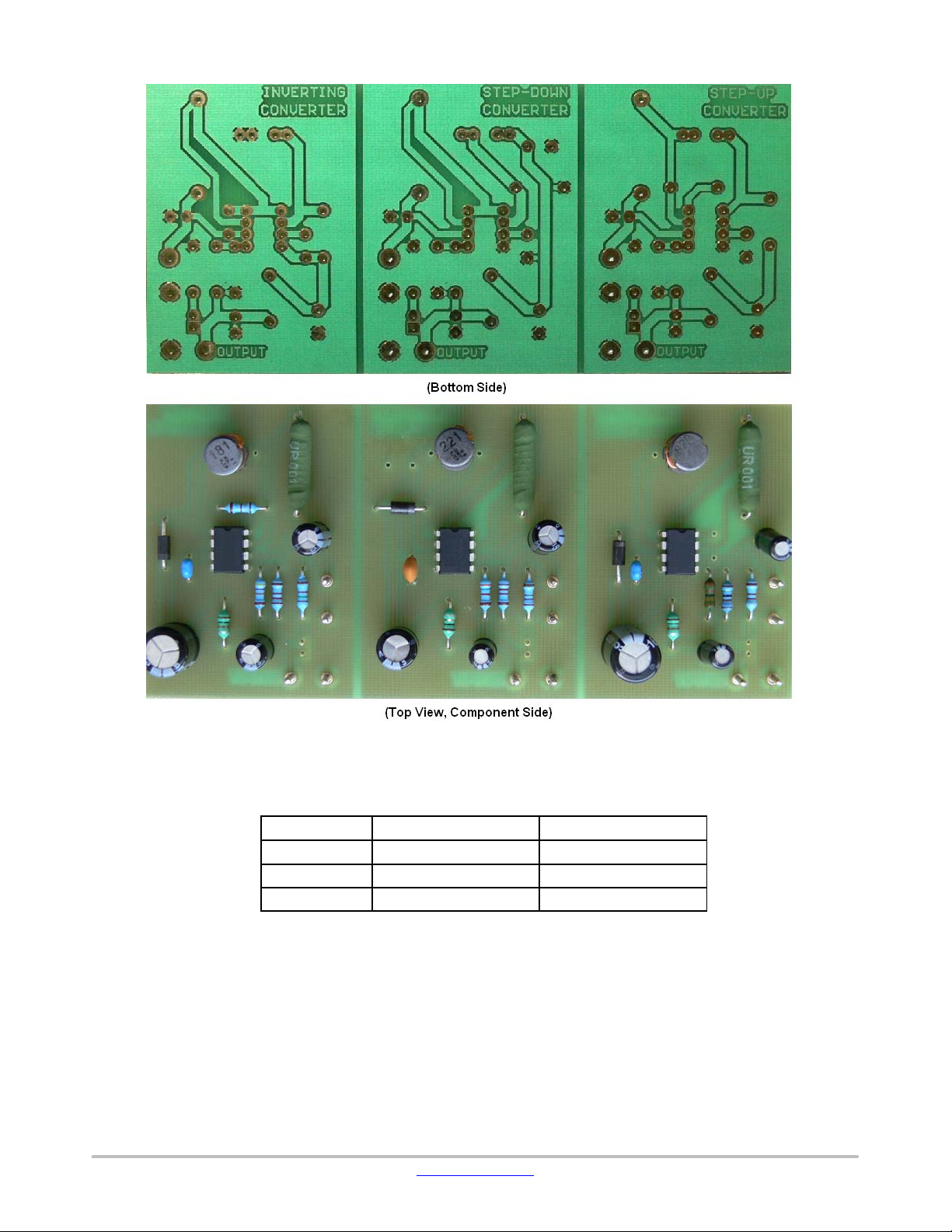
Figure 15. Printed Circuit Board and Component Layout
(Circuits of Figures 9, 11, 13)
INDUCTOR DATA
Converter
Step−Up 170 38 Turns of #22 AWG
Step−Down 220 48 Turns of #22 AWG
Voltage−Inverting 88 28 Turns of #22 AWG
All inductors are wound on Magnetics Inc. 55117 toroidal core.
Inductance (mH)
Turns/Wire
www.onsemi.com
9
Page 10
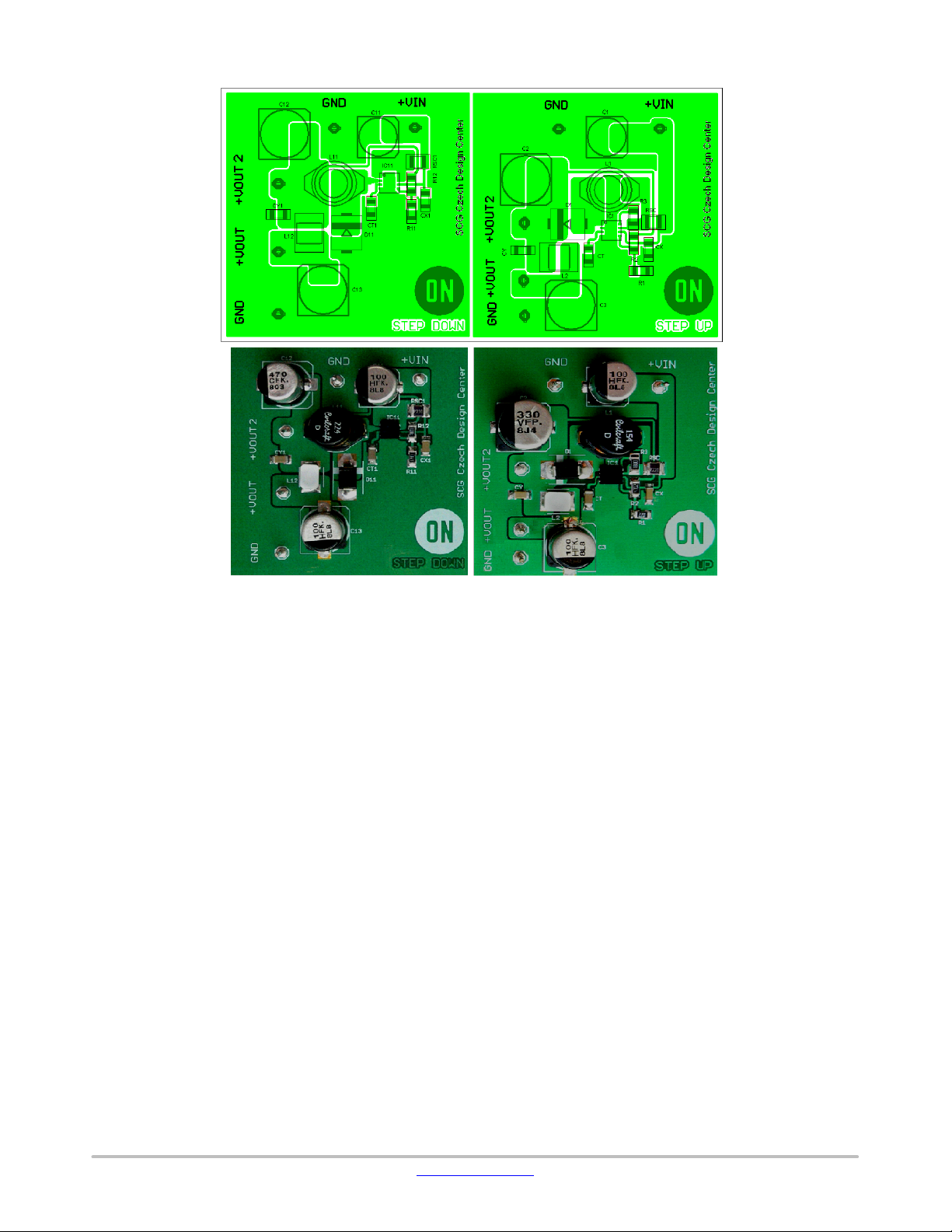
MC34063A, MC33063A, SC34063A, SC33063A, NCV33063A
Figure 16. Printed Circuit Board for DFN Device
www.onsemi.com
10
Page 11

MC34063A, MC33063A, SC34063A, SC33063A, NCV33063A
x)
Calculation
ton/t
off
(ton + t
t
off
t
on
C
T
I
pk(switch)
R
sc
L
(min)
)
off
ǒ
C
O
V
= Saturation voltage of the output switch.
sat
= Forward voltage drop of the output rectifier.
V
F
The following power supply characteristics must be chosen:
V
− Nominal input voltage.
in
V
− Desired output voltage,
out
I
− Desired output current.
out
− Minimum desired output switching frequency at the selected values of Vin and IO.
f
min
V
NOTE: For further information refer to Application Note AN920A/D and AN954/D.
− Desired peak−to−peak output ripple voltage. In practice, the calculated capacitor value will need to be increased due to its
ripple(pp)
equivalent series resistance and board layout. The ripple voltage should be kept to a low value since it will directly affect the
line and load regulation.
Step−Up Step−Down Voltage−Inverting
V
out
2I
out(max)
(V
in(min)
) VF* V
V
in(min)
ton) t
t
on
t
off
(ton + t
4.0 x 10⁻⁵ t
0.3/I
pk(switch)
* V
I
pk(switch)
I
out
9
V
ripple(pp)
|V
out
in(min)
* V
sat
1
f
off
) 1
) − t
off
off
on
t
on
ǒ
t
t
| + 1.25ǒ1 )
off
on
sat
) 1
)
Ǔ
Ǔ
t
on(max)
R2
R1
Ǔ
ǒ
(V
in(min)
V
in(min)
(ton + t
4.0 x 10⁻⁵ t
* V
I
pk(switch)
I
pk(switch)
V
out
* V
ton) t
t
on
t
off
2I
out(max)
0.3/I
sat
8V
ripple(pp)
) V
sat
1
f
) 1
) − t
off
pk(switch)
* V
(ton) t
off
off
on
F
* V
out
)
off
Ǔ
out
t
on(ma
)
ǒ
2I
(V
in(min)
|V
out
Vin* V
ton) t
t
on
t
off
(ton + t
4.0 x 10⁻⁵ t
out(max)
0.3/I
* V
I
pk(switch)
9
V
| ) V
sat
1
f
off
) 1
) − t
off
t
on
ǒ
t
off
pk(switch)
)
sat
I
t
on
out
ripple(pp)
F
off
on
) 1
Ǔ
t
Ǔ
on(max)
Figure 17. Design Formula Table
www.onsemi.com
11
Page 12
MC34063A, MC33063A, SC34063A, SC33063A, NCV33063A
ORDERING INFORMATION
Device Package Shipping
MC33063ADG SOIC−8
MC33063ADR2G SOIC−8
SC33063ADR2G SOIC−8
MC33063AP1G PDIP−8
MC33063AVDG SOIC−8
MC33063AVDR2G SOIC−8
NCV33063AVDR2G* SOIC−8
MC33063AVPG PDIP−8
MC34063ADG SOIC−8
MC34063ADR2G SOIC−8
SC34063ADR2G SOIC−8
MC34063AP1G PDIP−8
SC34063AP1G PDIP−8
MC33063MNTXG DFN8
†For information on tape and reel specifications, including part orientation and tape sizes, please refer to our Tape and Reel Packaging
Specification Brochure, BRD8011/D.
*NCV33063A: T
change control.
= −40°C, T
low
= +125°C. Guaranteed by design. NCV prefix is for automotive and other applications requiring site and
high
(Pb−Free)
(Pb−Free)
(Pb−Free)
(Pb−Free)
(Pb−Free)
(Pb−Free)
(Pb−Free)
(Pb−Free)
(Pb−Free)
(Pb−Free)
(Pb−Free)
(Pb−Free)
(Pb−Free)
(Pb−Free)
98 Units / Rail
2500 Units / Tape & Reel
2500 Units / Tape & Reel
50 Units / Rail
98 Units / Rail
2500 Units / Tape & Reel
50 Units / Rail
98 Units / Rail
2500 Units / Tape & Reel
2500 Units / Tape & Reel
50 Units / Rail
50 Units / Rail
4000 Units / Tape & Reel
†
www.onsemi.com
12
Page 13
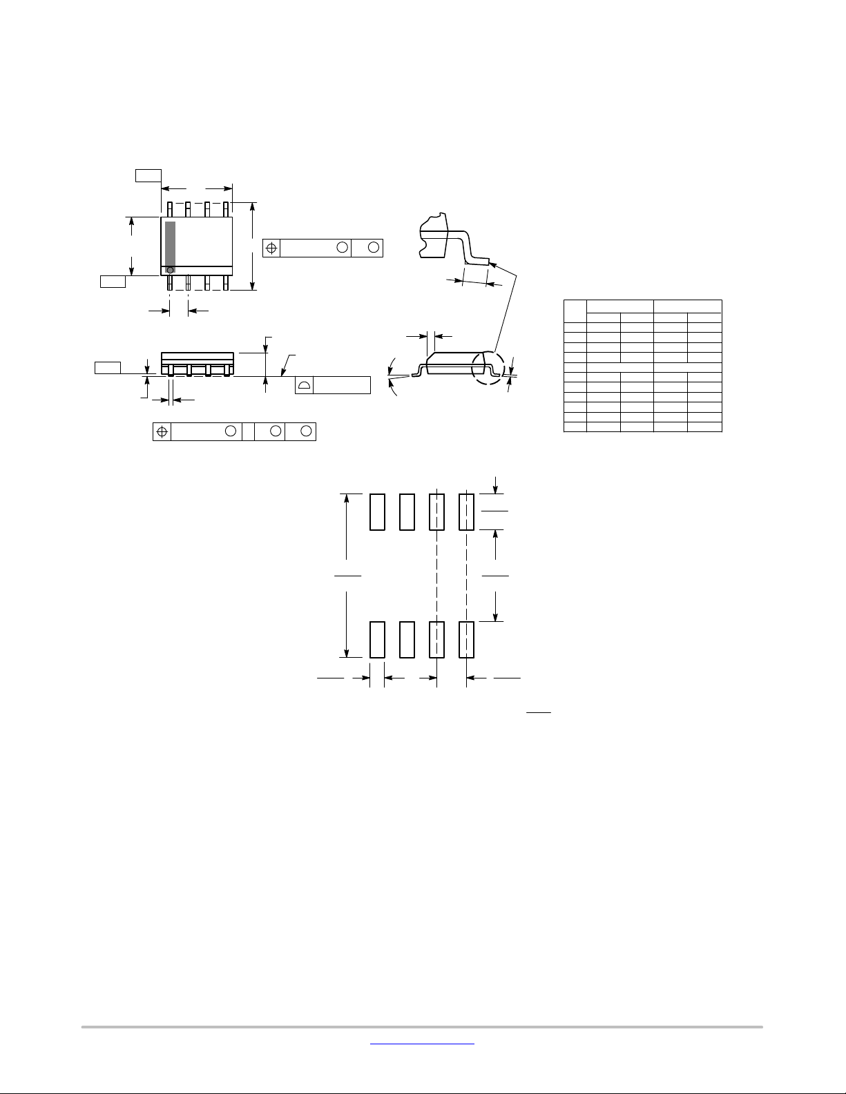
−Y−
−Z−
MC34063A, MC33063A, SC34063A, SC33063A, NCV33063A
PACKAGE DIMENSIONS
SOIC−8 NB
CASE 751−07
ISSUE AK
−X−
B
H
A
58
1
4
G
D
0.25 (0.010) Z
M
S
Y
0.25 (0.010)
C
SEATING
PLANE
SXS
M
0.10 (0.004)
M
Y
K
N
X 45
_
M
J
NOTES:
1. DIMENSIONING AND TOLERANCING PER
ANSI Y14.5M, 1982.
2. CONTROLLING DIMENSION: MILLIMETER.
3. DIMENSION A AND B DO NOT INCLUDE
MOLD PROTRUSION.
4. MAXIMUM MOLD PROTRUSION 0.15 (0.006)
PER SIDE.
5. DIMENSION D DOES NOT INCLUDE DAMBAR
PROTRUSION. ALLOWABLE DAMBAR
PROTRUSION SHALL BE 0.127 (0.005) TOTAL
IN EXCESS OF THE D DIMENSION AT
MAXIMUM MATERIAL CONDITION.
6. 751−01 THRU 751−06 ARE OBSOLETE. NEW
STANDARD IS 751−07.
MILLIMETERS
DIMAMIN MAX MIN MAX
4.80 5.00 0.189 0.197
B 3.80 4.00 0.150 0.157
C 1.35 1.75 0.053 0.069
D 0.33 0.51 0.013 0.020
G 1.27 BSC 0.050 BSC
H 0.10 0.25 0.004 0.010
J 0.19 0.25 0.007 0.010
K 0.40 1.27 0.016 0.050
M 0 8 0 8
____
N 0.25 0.50 0.010 0.020
S 5.80 6.20 0.228 0.244
INCHES
SOLDERING FOOTPRINT*
1.52
0.060
7.0
0.275
0.6
0.024
*For additional information on our Pb−Free strategy and soldering
details, please download the ON Semiconductor Soldering and
Mounting Techniques Reference Manual, SOLDERRM/D.
4.0
0.155
1.270
0.050
SCALE 6:1
ǒ
inches
mm
Ǔ
www.onsemi.com
13
Page 14
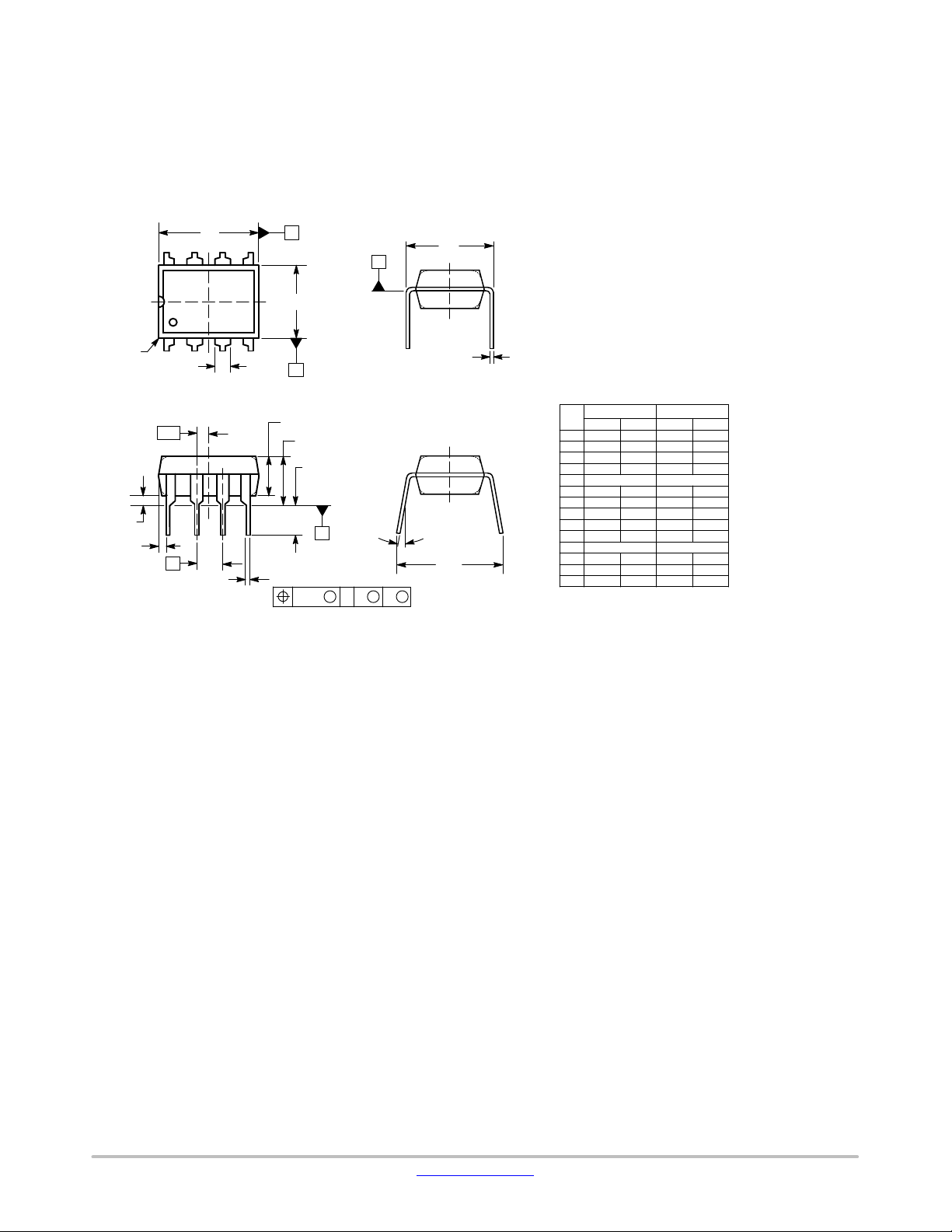
MC34063A, MC33063A, SC34063A, SC33063A, NCV33063A
PDIP−8
PACKAGE DIMENSIONS
P, P1 SUFFIX
CASE 626−05
ISSUE P
NOTE 8
A1
D1
D
A
58
E1
14
b2
B
TOP VIEW
e/2
A2
A
L
e
8X
b
SIDE VIEW
0.010 CA
NOTE 3
SEATING
PLANE
C
M
H
E
END VIEW
WITH LEADS CONSTRAINED
NOTE 5
M
eB
END VIEW
MBM
NOTE 6
NOTES:
1. DIMENSIONING AND TOLERANCING PER ASME Y14.5M, 1994.
2. CONTROLLING DIMENSION: INCHES.
3. DIMENSIONS A, A1 AND L ARE MEASURED WITH THE PACKAGE SEATED IN JEDEC SEATING PLANE GAUGE GS−3.
4. DIMENSIONS D, D1 AND E1 DO NOT INCLUDE MOLD FLASH
OR PROTRUSIONS. MOLD FLASH OR PROTRUSIONS ARE
NOT TO EXCEED 0.10 INCH.
5. DIMENSION E IS MEASURED AT A POINT 0.015 BELOW DATUM
PLANE H WITH THE LEADS CONSTRAINED PERPENDICULAR
TO DATUM C.
6. DIMENSION eB IS MEASURED AT THE LEAD TIPS WITH THE
LEADS UNCONSTRAINED.
c
7. DATUM PLANE H IS COINCIDENT WITH THE BOTTOM OF THE
LEADS, WHERE THE LEADS EXIT THE BODY.
8. PACKAGE CONTOUR IS OPTIONAL (ROUNDED OR SQUARE
CORNERS).
INCHES
DIM MIN MAX
A −−−− 0.210
A1 0.015 −−−−
A2 0.115 0.195 2.92 4.95
b 0.014 0.022
b2
0.060 TYP 1.52 TYP
C 0.008 0.014
D 0.355 0.400
D1 0.005 −−−−
E 0.300 0.325
E1 0.240 0.280 6.10 7.11
e 0.100 BSC
eB −−−− 0.430 −−− 10.92
L 0.115 0.150 2.92 3.81
M −−−− 10
MILLIMETERS
MIN MAX
−−− 5.33
0.38 −−−
0.35 0.56
0.20 0.36
9.02 10.16
0.13 −−−
7.62 8.26
2.54 BSC
−−− 10
°°
www.onsemi.com
14
Page 15
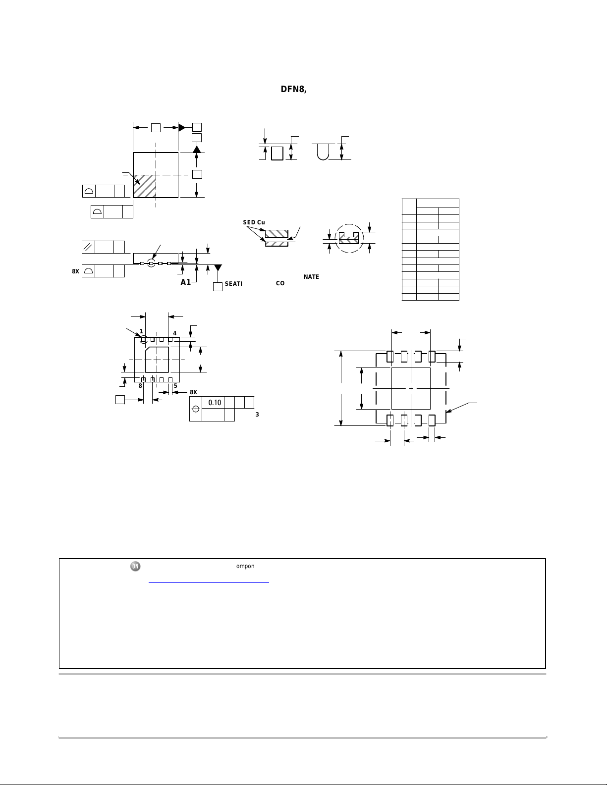
REFERENCE
P
al
2X
2X
8X
NOTE 4
PIN ONE
MC34063A, MC33063A, SC34063A, SC33063A, NCV33063A
PACKAGE DIMENSIONS
DFN8, 4x4
CASE 488AF−01
ISSUE C
NOTES:
1. DIMENSIONS AND TOLERANCING PER
ASME Y14.5M, 1994.
2. CONTROLLING DIMENSION: MILLIMETERS.
3. DIMENSION b APPLIES TO PLATED
TERMINAL AND IS MEASURED BETWEEN
0.15 AND 0.30MM FROM TERMINAL TIP.
4. COPLANARITY APPLIES TO THE EXPOSED
PAD AS WELL AS THE TERMINALS.
5. DETAILS A AND B SHOW OPTIONAL
CONSTRUCTIONS FOR TERMINALS.
A3
DIM MIN MAX
A 0.80 1.00
A1 0.00 0.05
A3 0.20 REF
b 0.25 0.35
D 4.00 BSC
D2 1.91 2.21
E 4.00 BSC
E2 2.09 2.39
e 0.80 BSC
K 0.20 −−−
L 0.30 0.50
L1 −−− 0.15
C0.15
C0.15
C0.10
C0.08
SIDE VIEW
D
TOP VIEW
DETAIL B
(A3)
A1
A
B
L
L
L1
E
A
SEATING
C
PLANE
DETAIL A
OPTIONAL
CONSTRUCTIONS
MOLD CMPDEXPOSED Cu
DETAIL B
ALTERNATE
CONSTRUCTIONS
A1
MILLIMETERS
DETAIL A
D2
1
8X L
4
SOLDERING FOOTPRINT*
2.21
8X
0.63
E2
K
e
BOTTOM VIEW
58
8X
b
0.10 C
0.05 C
AB
NOTE 3
4.30
2.39
0.80
PITCH
PACKAGE
OUTLINE
8X
0.35
DIMENSIONS: MILLIMETERS
*For additional information on our Pb−Free strategy and soldering
details, please download the ON Semiconductor Soldering and
Mounting Techniques Reference Manual, SOLDERRM/D.
SENSEFET is a trademark of Semiconductor Components Industries, LLC.
ON Semiconductor and are trademarks of Semiconductor Components Industries, LLC dba ON Semiconductor or its subsidiaries in the United States and/or other countries.
ON Semiconductor owns the rights to a number of patents, trademarks, copyrights, trade secrets, and other intellectual property. A listing of ON Semiconductor’s product/patent
coverage may be accessed at www.onsemi.com/site/pdf/Patent−Marking.pdf
ON Semiconductor makes no warranty, representation or guarantee regarding the suitability of its products for any particular purpose, nor does ON Semiconductor assume any liability
arising out of the application or use of any product or circuit, and specifically disclaims any and all liability, including without limitation special, consequential or incidental damages.
Buyer is responsible for its products and applications using ON Semiconductor products, including compliance with all laws, regulations and safety requirements or standards,
regardless of any support or applications information provided by ON Semiconductor. “Typical” parameters which may be provided in ON Semiconductor data sheets and/or
specifications can and do vary in different applications and actual performance may vary over time. All operating parameters, including “Typicals” must be validated for each customer
application by customer’s technical experts. ON Semiconductor does not convey any license under its patent rights nor the rights of others. ON Semiconductor products are not
designed, intended, or authorized for use as a critical component in life support systems or any FDA Class 3 medical devices or medical devices with a same or similar classification
in a foreign jurisdiction or any devices intended for implantation in the human body. Should Buyer purchase or use ON Semiconductor products for any such unintended or unauthorized
application, Buyer shall indemnify and hold ON Semiconductor and its officers, employees, subsidiaries, affiliates, and distributors harmless against all claims, costs, damages, and
expenses, and reasonable attorney fees arising out of, directly or indirectly, any claim of personal injury or death associated with such unintended or unauthorized use, even if such
claim alleges that ON Semiconductor was negligent regarding the design or manufacture of the part. ON Semiconductor is an Equal Opportunity/Affirmative Action Employer. This
literature is subject to all applicable copyright laws and is not for resale in any manner.
. ON Semiconductor reserves the right to make changes without further notice to any products herein.
UBLICATION ORDERING INFORMATION
LITERATURE FULFILLMENT:
Literature Distribution Center for ON Semiconductor
19521 E. 32nd Pkwy, Aurora, Colorado 80011 USA
Phone: 303−675−2175 or 800−344−3860 Toll Free USA/Canada
Fax: 303−675−2176 or 800−344−3867 Toll Free USA/Canada
Email: orderlit@onsemi.com
◊
N. American Technical Support: 800−282−9855 Toll Free
USA/Canada
Europe, Middle East and Africa Technical Support:
Phone: 421 33 790 2910
Japan Customer Focus Center
Phone: 81−3−5817−1050
www.onsemi.com
ON Semiconductor Website: www.onsemi.com
Order Literature: http://www.onsemi.com/orderlit
For additional information, please contact your loc
Sales Representative
MC34063A/D
15
 Loading...