

Datasheet MC34063AMEL, MC34063AML1, MC34063AML2, MC34063AP1, MC34063AD Datasheet (Motorola)
...Page 1
The MC34063A Series is a monolithic control circuit containing the
primary functions required for DC–to–DC converters. These devices consist
of an internal temperature compensated reference, comparator, controlled
duty cycle oscillator with an active current limit circuit, driver and high current
output switch. This series was specifically designed to be incorporated in
Step–Down and Step–Up and Voltage–Inverting applications with a
minimum number of external components. Refer to Application Notes
AN920A/D and AN954/D for additional design information.
• Operation from 3.0 V to 40 V Input
• Low Standby Current
• Current Limiting
• Output Switch Current to 1.5 A
• Output Voltage Adjustable
• Frequency Operation to 100 kHz
• Precision 2% Reference
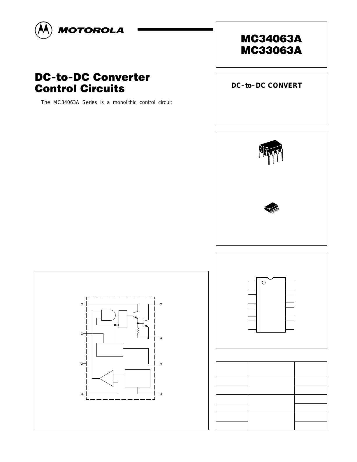
Order this document by MC34063A/D
DC–to–DC CONVERTER
CONTROL CIRCUITS
SEMICONDUCTOR
TECHNICAL DATA
8
1
P, P1 SUFFIX
PLASTIC PACKAGE
CASE 626
8
1
D SUFFIX
PLASTIC PACKAGE
CASE 751
(SO–8)
Representative Schematic Diagram
8
Drive
Collector
SQ
R
I
pk
C
T
Comparator
+
–
(Bottom View)
100
1.25 V
Reference
Regulator
I
pk
Sense
V
CC
Comparator
Inverting
Input
This device contains 51 active transistors.
7
Oscillator
6
MOTOROLA ANALOG IC DEVICE DATA
Q2
Q1
1
Switch
Collector
2
Switch
Emitter
3
Timing
Capacitor
45
Gnd
PIN CONNECTIONS
Switch
Collector
Switch
Emitter
Timing
Capacitor
Gnd
1
2
3
45
(Top View)
Driver
8
Collector
7
Ipk Sense
6
V
CC
Comparator
Inverting
Input
ORDERING INFORMATION
Operating
Device
MC33063AD
MC33063AP1
MC33063AVD
MC33063AVP Plastic DIP
MC34063AD SO–8
MC34063AP1
Motorola, Inc. 1996 Rev 5
Temperature Range
TA = – 40° to +85°C
TA = –40° to +125°C
TA = 0° to +70°C
Package
SO–8
Plastic DIP
SO–8
Plastic DIP
1
Page 2
MC34063A MC33063A
MAXIMUM RATINGS
Rating Symbol Value Unit
Power Supply Voltage V
Comparator Input Voltage Range V
Switch Collector Voltage V
Switch Emitter Voltage (V
= 40 V) V
Pin 1
Switch Collector to Emitter Voltage V
Driver Collector Voltage V
Driver Collector Current (Note 1) I
Switch Current I
Power Dissipation and Thermal Characteristics
Plastic Package, P, P1 Suffix
TA = 25°C P
Thermal Resistance R
SOIC Package, D Suffix
TA = 25°C P
Thermal Resistance R
Operating Junction Temperature T
Operating Ambient Temperature Range T
MC34063A 0 to +70
MC33063AV –40 to +125
MC33063A –40 to +85
Storage Temperature Range T
NOTES: 1. Maximum package power dissipation limits must be observed.
2.ESD data available upon request.
CC
IR
C(switch)
E(switch)
CE(switch)
C(driver)
C(driver)
SW
D
θJA
D
θJA
J
A
stg
–0.3 to +40 Vdc
–65 to +150 °C
40 Vdc
40 Vdc
40 Vdc
40 Vdc
40 Vdc
100 mA
1.5 A
1.25 W
100 °C/W
625 W
160 °C/W
+150 °C
°C
ELECTRICAL CHARACTERISTICS (V
= 5.0 V, TA = T
CC
low
to T
[Note 3], unless otherwise specified.)
high
Characteristics Symbol Min Typ Max Unit
OSCILLATOR
Frequency (V
Charge Current (VCC = 5.0 V to 40 V, TA = 25°C) I
Discharge Current (VCC = 5.0 V to 40 V, TA = 25°C) I
Discharge to Charge Current Ratio (Pin 7 to VCC, TA = 25°C) I
Current Limit Sense Voltage (I
= 0 V, CT = 1.0 nF, TA = 25°C) f
Pin 5
chg
= I
, TA = 25°C) V
dischg
osc
chg
dischg
dischg/Ichg
ipk(sense)
24 33 42 kHz
24 35 42 µA
140 220 260 µA
5.2 6.5 7.5 –
250 300 350 mV
OUTPUT SWITCH (Note 4)
Saturation Voltage, Darlington Connection (Note 5)
(ISW = 1.0 A, Pins 1, 8 connected)
Saturation Voltage, Darlington Connection
(ISW = 1.0 A, R
= 82 Ω to VCC, Forced β ] 20)
Pin 8
DC Current Gain (ISW = 1.0 A, VCE = 5.0 V, TA = 25°C) h
Collector Off–State Current (VCE = 40 V) I
NOTES: 3. T
= 0°C for MC34063A, –40°C for MC33063A, AV T
low
4.Low duty cycle pulse techniques are used during test to maintain junction temperature as close to ambient temperature as possible.
5.If the output switch is driven into hard saturation (non–Darlington configuration) at low switch currents (≤ 300 mA) and high driver currents (≥ 30 mA),
it may take up to 2.0 µs for it to come out of saturation. This condition will shorten the off time at frequencies ≥ 30 kHz, and is magnified at high
temperatures. This condition does not occur with a Darlington configuration, since the output switch cannot saturate. If a non–Darlington
configuration is used, the following output drive condition is recommended:
Forcedbof output switch :
*The 100 Ω resistor in the emitter of the driver device requires about 7.0 mA before the output switch conducts.
ICoutput
ICdriver – 7.0 mA *
w
10
= +70°C for MC34063A, +85°C for MC33063A, +125°C for MC33063AV
high
V
CE(sat)
V
CE(sat)
FE
C(off)
– 1.0 1.3 V
– 0.45 0.7 V
50 75 – –
– 0.01 100 µA
2
MOTOROLA ANALOG IC DEVICE DATA
Page 3
MC34063A MC33063A
ELECTRICAL CHARACTERISTICS (continued) (V
= 5.0 V, TA = T
CC
low
to T
[Note 3], unless otherwise specified.)
high
Characteristics UnitMaxTypMinSymbol
COMPARATOR
Threshold Voltage
TA = 25°C
TA = T
low
to T
high
Threshold Voltage Line Regulation (VCC = 3.0 V to 40 V)
MC33063A, MC34063A
MC33363A V
Input Bias Current (Vin = 0 V) I
Reg
V
th
1.225
1.25–1.275
1.21
line
IB
–
–
1.4
1.4
– –20 –400 nA
TOTAL DEVICE
Supply Current (VCC = 5.0 V to 40 V, CT = 1.0 nF, Pin 7 = VCC,
V
> Vth, Pin 2 = Gnd, remaining pins open)
Pin 5
NOTES: 3. T
= 0°C for MC34063A, –40°C for MC33063A, AV T
low
4.Low duty cycle pulse techniques are used during test to maintain junction temperature as close to ambient temperature as possible.
5.If the output switch is driven into hard saturation (non–Darlington configuration) at low switch currents (≤ 300 mA) and high driver currents (≥ 30 mA),
it may take up to 2.0 µs for it to come out of saturation. This condition will shorten the off time at frequencies ≥ 30 kHz, and is magnified at high
temperatures. This condition does not occur with a Darlington configuration, since the output switch cannot saturate. If a non–Darlington
configuration is used, the following output drive condition is recommended:
Forcedbof output switch :
*The 100 Ω resistor in the emitter of the driver device requires about 7.0 mA before the output switch conducts.
ICoutput
ICdriver – 7.0 mA *
w
10
= +70°C for MC34063A, +85°C for MC33063A, +125°C for MC33063AV
high
I
CC
– – 4.0 mA
V
1.29
mV
5.0
6.0
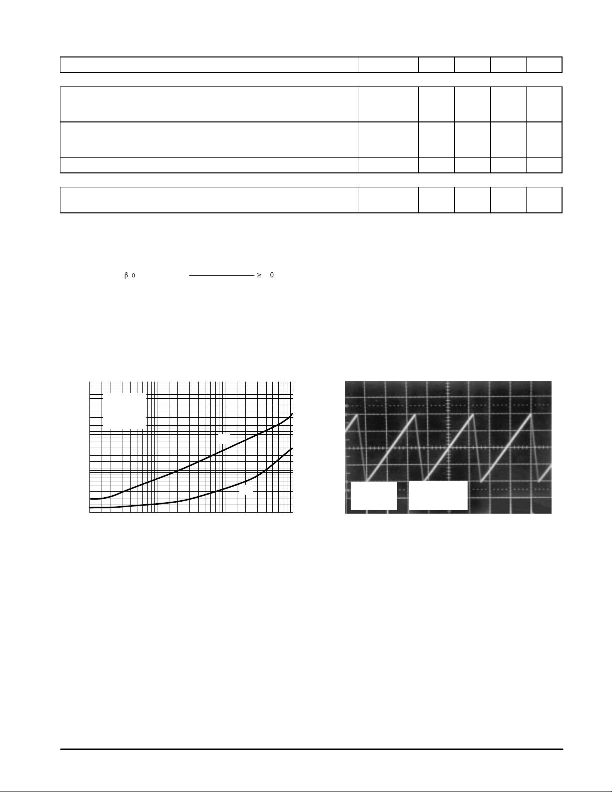
Figure 1. Output Switch On–Off Time versus
Oscillator Timing Capacitor
1000
µ
VCC = 5.0 V
500
Pin 7 = V
200
100
50
20
10
5.0
, OUTPUT SWITCH ON-OFF TIME ( s)
2.0
on–off
1.0
t
0.01 0.02 0.05 0.1 0.2 0.5 1.0 2.0 5.0 10
CC
Pin 5 = Gnd
°
C
TA = 25
CT, OSCILLAT OR TIMING CAPACITOR (nF)
t
on
t
off
, OSCILLAT OR VOLTAGE (V)
VCC = 5.0 V
OSC
Pin 7 = V
V
Pin 2 = Gnd
Figure 2. Timing Capacitor Waveform
Pins 1, 5, 8 = Open
CC
CT = 1.0 nF
°
C
TA = 25
10 µs/DIV
200 mV/DIV
MOTOROLA ANALOG IC DEVICE DATA
3
Page 4
Figure 3. Emitter Follower Configuration Output
Saturation V oltage versus Emitter Current
1.8
1.7
1.6
1.5
1.4
1.3
, SATURATION VOLTAGE (V)
1.2
1.1
CE(sat)
V
1.0
0 0.2 0.4 0.6 0.8 1.0 1.2 1.4 1.6
IE, EMITTER CURRENT (A)
VCC = 5.0 V
Pins 1, 7, 8 = V
Pins 3, 5 = Gnd
TA = 25
(See Note 4)
MC34063A MC33063A
Figure 4. Common Emitter Configuration Output
1.1
1.0
0.9
0.8
0.7
0.6
VCC = 5.0 V
Pin 7 = V
0.5
Pins 2, 3, 5 = Gnd
0.4
CC
°
C
, SATURATION VOLTAGE (V)
V
TA = 25
0.3
(See Note 4)
0.2
CE(sat)
0.1
0
0 0.2 0.4 0.6 0.8 1.0 1.2 1.4 1.6
Switch Saturation Voltage versus
Collector Current
Darlington Connection
CC
°
C
IC, COLLECTOR CURRENT(A)
Forced
β
= 20
Figure 5. Current Limit Sense V oltage
versus T emperature
400
380
VCC = 5.0 V
360
I
= I
chg
340
320
300
280
260
, CURRENT LIMIT SENSE VOLTAGE (V)
240
220
200
IPK(sense)
–55 –25 0 25 50 75 100 125
V
NOTE: 4.Low duty cycle pulse techniques are used during test to maintain junction temperature as close to ambient temperature as possible.
dischg
TA, AMBIENT TEMPERATURE (°C)
, SUPPLY CURRENT (mA)
CC
I
Figure 6. Standby Supply Current versus
Supply V oltage
3.6
3.2
2.8
2.4
2.0
1.6
1.2
0.8
0.4
0
0 5.0 10 15 20 25 30 35 40
VCC, SUPPLY VOLTAGE (V)
CT = 1.0 nF
Pin 7 = V
Pin 2 = Gnd
CC
4
MOTOROLA ANALOG IC DEVICE DATA
Page 5

MC34063A MC33063A
Figure 7. Step–Up Converter
170 µH
L
8
180
SQRQ2
7
I
R
sc
0.22
V
in
12 V
Line Regulation Vin = 8.0 V to 16 V, IO = 175 mA 30 mV = ±0.05%
Load Regulation Vin = 12 V, IO = 75 mA to 175 mA 10 mV = ±0.017%
Output Ripple Vin = 12 V, IO = 175 mA 400 mVpp
Efficiency Vin = 12 V, IO = 175 mA 87.7%
Output Ripple With Optional Filter Vin = 12 V, IO = 175 mA 40 mVpp
6
+
100
5
R1 2.2 k
Test Conditions Results
pk
V
CC
+
Comp.
–
R2
47 k
Osc
C
T
1.25 V
Ref
Reg
Q1
1
2
3
C
T
1500
pF
4
330 C
1N5819
28 V/175 mA
+
O
V
out
µ
H
1.0
+
Optional Filter
100
V
out
Figure 8. External Current Boost Connections for IC Peak Greater than 1.5 A
8a. External NPN Switch 8b. External NPN Saturated Switch
(See Note 5)
V
8
7
R
sc
V
in
NOTE: 5.If the output switch is driven into hard saturation (non–Darlington configuration) at low switch currents (≤ 300 mA) and high driver currents
6
(≥ 30 mA), it may take up to 2.0 µs to come out of saturation. This condition will shorten the off time at frequencies ≥ 30 kHz, and is magnified
at high temperatures. This condition does not occur with a Darlington configuration, since the output switch cannot saturate. If a non–Darlington
configuration is used, the following output drive condition is recommended.
1
2
out
8
7
R
sc
V
in
6
1
2
R
R
constant V
MOTOROLA ANALOG IC DEVICE DATA
³
0 for
V
out
in
5
Page 6

MC34063A MC33063A
Figure 9. Step–Down Converter
Q1
1
2
1N5819
3
C
T
470
pF
4
470 C
L
220
µ
H
1.0
+
O
V
out
5.0 V/500 mA
8
SQ
R
7
I
R
sc
0.33
V
in
25 V
100
Line Regulation Vin = 15 V to 25 V, IO = 500 mA 12 mV = ±0.12%
Load Regulation Vin = 25 V, IO = 50 mA to 500 mA 3.0 mV = ±0.03%
Output Ripple Vin = 25 V, IO = 500 mA 120 mVpp
Short Circuit Current Vin = 25 V, RL = 0.1 Ω 1.1 A
Efficiency Vin = 25 V, IO = 500 mA 83.7%
Output Ripple With Optional Filter Vin = 25 V, IO = 500 mA 40 mVpp
6
+
5
R1 1.2 k
pk
Osc
V
CC
+
Comp.
–
R2
3.6 k
Test Conditions Results
Q2
C
T
1.25 V
Ref
Reg
µ
H
+
100
Optional Filter
V
out
Figure 10. External Current Boost Connections for IC Peak Greater than 1.5 A
10a. External NPN Switch 10b. External PNP Saturated Switch
8
7
R
sc
V
in
6
6
1
2
V
out
8
7
R
sc
V
in
6
MOTOROLA ANALOG IC DEVICE DATA
1
2
V
out
Page 7

MC34063A MC33063A
Figure 11. Voltage Inverting Converter
0.24
V
4.5 V to 6.0 V
in
100
Line Regulation Vin = 4.5 V to 6.0 V, IO = 100 mA 3.0 mV = ±0.012%
Load Regulation Vin = 5.0 V, IO = 10 mA to 100 mA 0.022 V = ±0.09%
Output Ripple Vin = 5.0 V, IO = 100 mA 500 mVpp
Short Circuit Current Vin = 5.0 V, RL = 0.1 Ω 910 mA
Efficiency Vin = 5.0 V, IO = 100 mA 62.2%
Output Ripple With Optional Filter Vin = 5.0 V, IO = 100 mA 70 mVpp
R
sc
+
R2 8.2 k
Q1
1
2
88 µH
L
3
+
1500
pF
4
1000
1N5819
V
out
–12 V/100 mA
µ
f
C
O
+
8
SQRQ2
7
I
pk
6
V
CC
+
–
5
953
Test Conditions Results
Osc
Comp.
R1
C
T
1.25 V
Ref
Reg
1.0
µ
H
+
Optional Filter
100
V
out
Figure 12. External Current Boost Connections for IC Peak Greater than 1.5 A
12a. External NPN Switch 12b. External PNP Saturated Switch
8
7
V
in
6
1
2
MOTOROLA ANALOG IC DEVICE DATA
1
8
V
out
7
V
in
6
2
V
out
7
Page 8

MC34063A MC33063A
Figure 13. Printed Circuit Board and Component Layout
(Circuits of Figures 7, 9, 11)
5.45
′′
(Top view, copper foil as seen through the board from the component side)
2.500
′′
MC34063A
MC34063A
(Top View , Component Side)
INDUCTOR DATA
Converter Inductance (µH) Turns/Wire
Step–Up 170 38 Turns of #22 AWG
Step–Down 220 48 Turns of #22 AWG
Voltage–Inverting 88 28 Turns of #22 AWG
All inductors are wound on Magnetics Inc. 55117 toroidal core.
MC34063A
*Optional Filter.
8
MOTOROLA ANALOG IC DEVICE DATA
Page 9

MC34063A MC33063A
Figure 14. Design Formula T able
Calculation Step–Up Step–Down Voltage–Inverting
ton/t
off
(ton + t
I
pk(switch)
V
sat
VF = Forward voltage drop of the output rectifier.
The following power supply characteristics must be chosen:
Vin – Nominal input voltage.
V
out
I
out
f
min
V
ripple(pp)
V
ripple(pp)
NOTE: For further information refer to Application Note AN920A/D and AN954/D.
)
off
t
off
t
on
C
T
R
sc
L
(min)
C
O
= Saturation voltage of the output switch.
– Desired output voltage,
– Desired output current.
– Minimum desired output switching frequency at the selected values of Vin and IO.
– Desired peak–to–peak output ripple voltage. In practice, the calculated capacitor value will need to be increased due to its equivalent series
– resistance and board layout. The ripple voltage should be kept to a low value since it will directly affect the line and load regulation.
ǒ
V
2I
(V
out
in(min)
)
VF*
V
in(min)
ton)
t
on
t
off
(ton + t
4.0 x 10⁻⁵ t
out(max)
0.3/I
*
I
pk(switch)
9
V
|V
|+1.25
out
V
*
V
1
f
t
off
)
1
) – t
off
on
t
on
ǒ
t
off
pk(switch)
V
)
sat
I
t
on
out
ripple(pp)
in(min)
sat
off
)
t
Ǔ
on(max)
ǒ
1
)
|V
V
)
V
in(min)
ton)
t
t
(ton + t
4.0 x 10⁻⁵ t
2I
0.3/I
*
V
I
pk(switch)
I
pk(switch)
8V
out
on
off
sat
V
Ǔ
1
(V
in(min)
ǒ
R2
Ǔ
R1
*
V
sat
1
f
t
off
)
1
) – t
off
out(max)
pk(switch)
*
V
(ton)
ripple(pp)
F
on
out
*
off
V
)
t
off
out
Ǔ
)
t
on(max)
ǒ
2I
(V
in(min)
out(max)
I
pk(switch)
|)V
out
Vin*
1
f
ton)
t
on
)
t
off
(ton + t
off
4.0 x 10⁻⁵ t
ǒ
0.3/I
pk(switch)
*
V
sat
I
out
9
V
ripple(pp)
V
t
off
) – t
t
on
t
off
t
on
sat
1
on
)
Ǔ
F
off
)
t
Ǔ
1
on(max)
MOTOROLA ANALOG IC DEVICE DATA
9
Page 10

NOTE 2
–T–
SEATING
PLANE
58
14
F
–A–
D
H
G
0.13 (0.005)
MC34063A MC33063A
OUTLINE DIMENSIONS
–B–
C
N
K
M M M
T
P, P1 SUFFIX
PLASTIC PACKAGE
CASE 626–05
ISSUE K
L
AB
NOTES:
1. DIMENSION L TO CENTER OF LEAD WHEN
FORMED PARALLEL.
2. PACKAGE CONTOUR OPTIONAL (ROUND OR
SQUARE CORNERS).
3. DIMENSIONING AND TOLERANCING PER ANSI
Y14.5M, 1982.
MILLIMETERS INCHES
MIN MINMAX MAX
DIM
A
B
C
D
F
G
J
M
H
J
K
L
M
N
9.40
6.10
3.94
0.38
1.02
2.54 BSC
0.76
0.20
2.92
7.62 BSC
—
0.76
10.16
6.60
4.45
0.51
1.78
1.27
0.30
3.43
10
1.01
°
0.370
0.240
0.155
0.015
0.040
0.100 BSC
0.030
0.008
0.115
0.300 BSC
—
0.030
0.400
0.260
0.175
0.020
0.070
0.050
0.012
0.135
10
0.040
°
–T–
–A–
58
4X P
–B–
14
C
8X D
K
0.25 (0.010)MB
SEATING
PLANE
SS
A0.25 (0.010)MTB
D SUFFIX
PLASTIC PACKAGE
CASE 751–05
(SO–8)
ISSUE P
M
R
X 45
_
_
M
NOTES:
1. DIMENSIONING AND TOLERANCING PER
ANSI Y14.5M, 1982.
2. CONTROLLING DIMENSION: MILLIMETER.
3. DIMENSIONS A AND B DO NOT INCLUDE
MOLD PROTRUSION.
4. MAXIMUM MOLD PROTRUSION 0.15 (0.006)
PER SIDE.
5. DIMENSION D DOES NOT INCLUDE DAMBAR
PROTRUSION. ALLOWABLE DAMBAR
PROTRUSION SHALL BE 0.127 (0.005) TOTAL
IN EXCESS OF THE D DIMENSION AT
MAXIMUM MATERIAL CONDITION.
DIM MIN MAX MIN MAX
F
J
A 4.80 5.00 0.189 0.196
B 3.80 4.00 0.150 0.157
C 1.35 1.75 0.054 0.068
D 0.35 0.49 0.014 0.019
F 0.40 1.25 0.016 0.049
G 1.27 BSC 0.050 BSC
J 0.18 0.25 0.007 0.009
K 0.10 0.25 0.004 0.009
M 0 7 0 7
P 5.80 6.20 0.229 0.244
R 0.25 0.50 0.010 0.019
INCHESMILLIMETERS
____
10
MOTOROLA ANALOG IC DEVICE DATA
Page 11

MC34063A MC33063A
NOTES
MOTOROLA ANALOG IC DEVICE DATA
11
Page 12

MC34063A MC33063A
Motorola reserves the right to make changes without further notice to any products herein. Motorola makes no warranty , representation or guarantee regarding
the suitability of its products for any particular purpose, nor does Motorola assume any liability arising out of the application or use of any product or circuit, and
specifically disclaims any and all liability, including without limitation consequential or incidental damages. “T ypical” parameters which may be provided in Motorola
data sheets and/or specifications can and do vary in different applications and actual performance may vary over time. All operating parameters, including “Typicals”
must be validated for each customer application by customer’s technical experts. Motorola does not convey any license under its patent rights nor the rights of
others. Motorola products are not designed, intended, or authorized for use as components in systems intended for surgical implant into the body, or other
applications intended to support or sustain life, or for any other application in which the failure of the Motorola product could create a situation where personal injury
or death may occur. Should Buyer purchase or use Motorola products for any such unintended or unauthorized application, Buyer shall indemnify and hold Motorola
and its officers, employees, subsidiaries, affiliates, and distributors harmless against all claims, costs, damages, and expenses, and reasonable attorney fees
arising out of, directly or indirectly, any claim of personal injury or death associated with such unintended or unauthorized use, even if such claim alleges that
Motorola was negligent regarding the design or manufacture of the part. Motorola and are registered trademarks of Motorola, Inc. Motorola, Inc. is an Equal
Opportunity/Affirmative Action Employer.
How to reach us:
USA/EUROPE/Locations Not Listed: Motorola Literature Distribution; JAPAN: Nippon Motorola Ltd.; Tatsumi–SPD–JLDC, 6F Seibu–Butsuryu–Center,
P.O. Box 20912; Phoenix, Arizona 85036. 1–800–441–2447 or 602–303–5454 3–14–2 T atsumi Koto–Ku, Tokyo 135, Japan. 03–81–3521–8315
MFAX: RMF AX0@email.sps.mot.com – TOUCHT ONE 602–244–6609 ASIA/ PACIFIC: Motorola Semiconductors H.K. Ltd.; 8B Tai Ping Industrial Park,
INTERNET: http://Design–NET.com 51 Ting Kok Road, T ai Po, N.T., Hong Kong. 852–26629298
12
◊
MOTOROLA ANALOG IC DEVICE DATA
MC34063A/D
*MC34063A/D*
 Loading...