

Datasheet MC34063ABN, MC34063ACD, MC34063ACD-TR, MC34063ACN, MC34063ABD Datasheet (SGS Thomson Microelectronics)
...Page 1
DC-DC CONVERTER CONTROL CIRCUITS
■ OUTPUT SWITCHCURRENT IN EXCESSOF
1.5A
■ 2%REFERENCEACCURACY
■
LOWQUIESCENTCURRENT: 2.5mA(TYP.)
■ OPERATINGFROM3VTO 40V
■ FREQUENCYOPERATIONTO100KHz
■
ACTIVECURRENT LIMITING
DESCRIPTION
The MC34063A series is a monolithic control
circuit delivering the main functions for DC-DC
voltageconverting.
The device contains an internal temperature
compensated reference, comparator, duty cycle
controlled oscillator with an active current limit
circuit,driver and high current outputswitch.
Output voltage is adjustable through two external
resistorswitha 2% referenceaccuracy.
Employing a minimum number of external
components the MC34063A devices series is
designed for Step-Down, Step-Up and
Voltage-Invertingapplications.
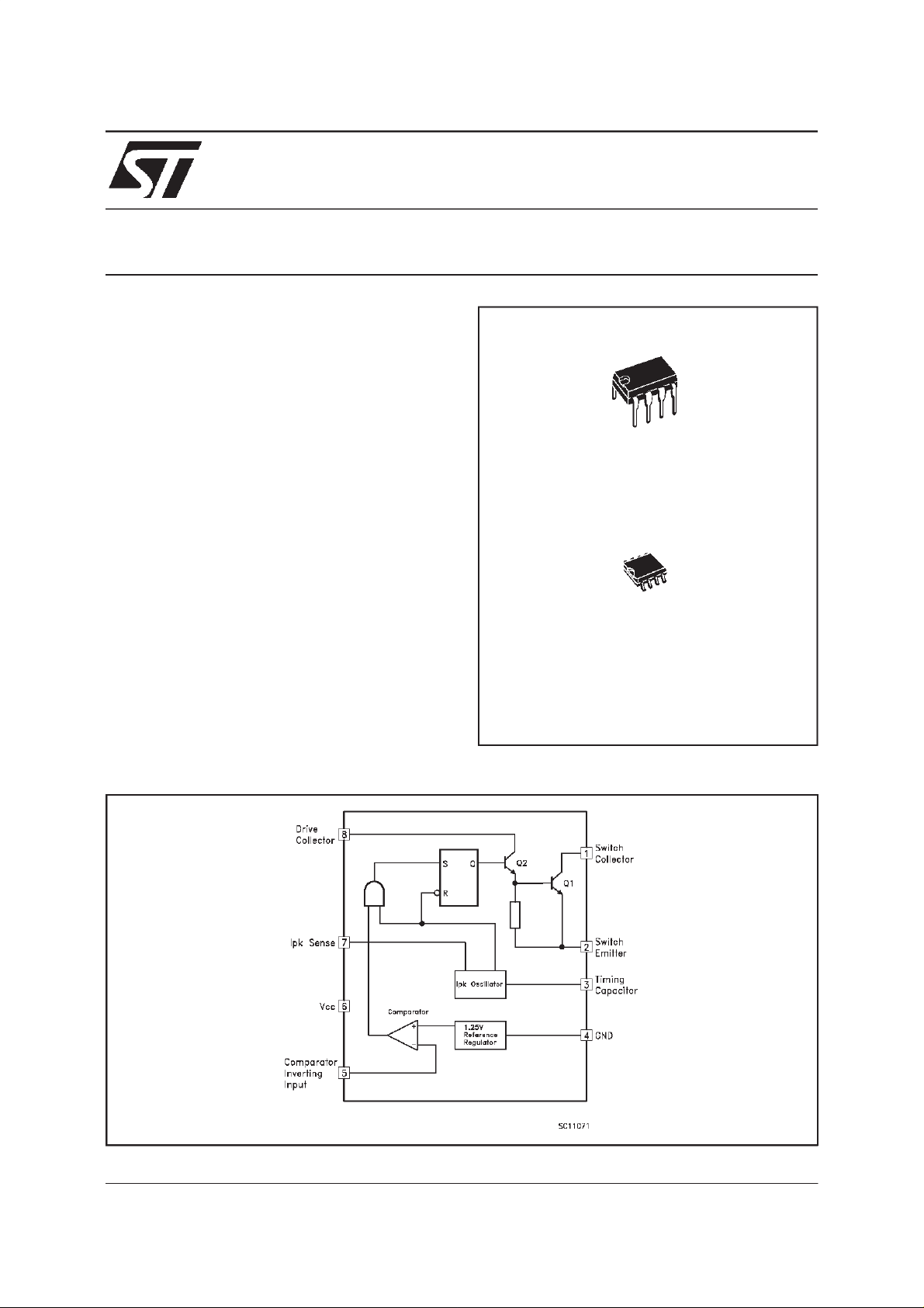
MC34063A
DIP-8
SO-8
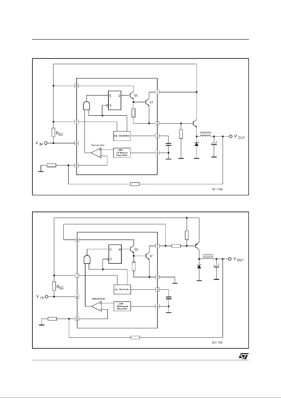
BLOCKDIAGRAM
April 2000
1/15
Page 2
MC34063A
ABSOLUTE MAXIMUM RATINGS
Symbol Parameter Value Unit
V
V
V
V
Absolute Maximum Rating are those values beyond which damage to the device may occur.
Functionaloperation under these condition is not implied.
THERMALDATA
PowerSupplyVoltage 50 V
CC
Comparator InputVoltage Range -0.3 to 40 V
V
ir
SwitchCollectorVoltage 40 V
SWC
SwitchEmitterVoltage(VSWC =40V) 40 V
SWE
SwitchEmitterto Collector Voltage 40 V
CE
DriverCollectorVoltage 40 V
V
dc
DriverCollectorCurrent 100 mA
I
dc
SwitchCurrent 1.5 A
I
SW
P
PowerDissipation at T
tot
OperatingAmbientTemperature Range (forAC SERIES)
T
op
StorageTemperature Range - 40 to 150
T
stg
=25oC (for
amb
PlasticPackage
(for SOICPackage)
(for ABSERIES)
)
1.25
0.625
0to70
-40to85
W
o
C
o
C
o
C
Symbol Parameter DIP-8 SO-8 Unit
R
thj-amb
(*) This value depends from thermal design ofPCB on which the device is mounted.
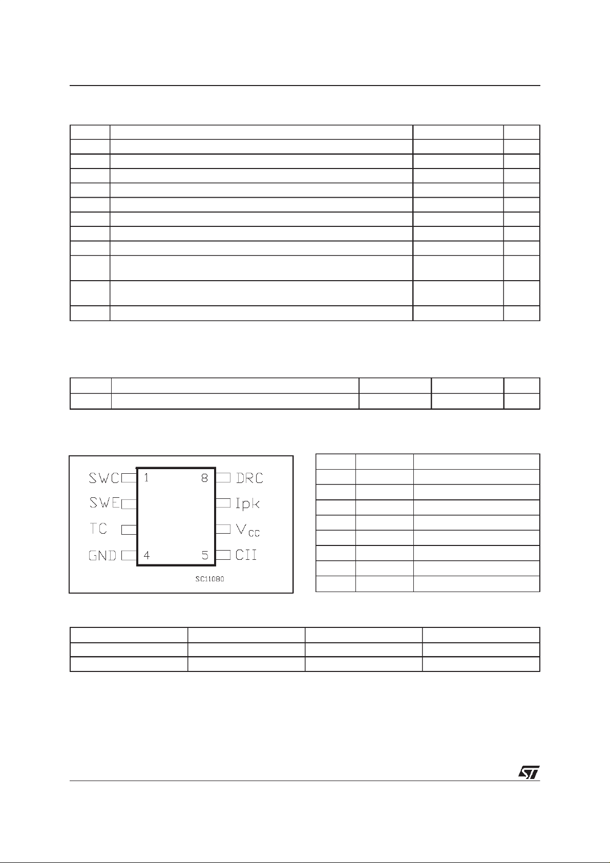
CONNECTION DIAGRAM
Thermal Resistance Junction-ambient (*) Max 100 160
(top view)
PIN CONNECTIONS
o
Pin No Symbol Name and Function
1 SWC SwitchCollector
2 SWE SwitchEmitter
3 TC TimingCapacitor
4 GND Ground
5 CII Comparator InvertingInput
6V
7I
CC
pk
Voltage Supply
IpkSense
8 DRC Voltage DriverCollector
ORDERING NUMBERS
Type DIP-8 SO-8 SO-8 (tape & reel)
MC34063AB MC34063ABN MC34063ABD MC34063ABD-TR
MC34063AC MC34063ACN MC34063ACD MC34063ACD-TR
C/W
2/15
Page 3
MC34063A
ELECTRICALCHARACTERISTICS
(Refer to the testcircuits,V
= 5V,Ta=T
CC
LOW
toT
HIGH
, unless
otherwisespecified,see note 2)
OSCILLATOR
Symbol Parameter Test Conditions Min. Typ. Max. Unit
f
OSC
I
I
dischg
I
dischg/Ichg
Frequency V
Charge Currernt VCC= 5 to 40V Ta=25oC 243342
chg
=0V CT= 1 nF Ta=25oC243342KHz
pin5
Discharge Current VCC= 5 to 40V Ta=25oC 140 200 260
Discharge toCharge
Pin 7 = V
CCTa
=25oC 5.2 6.2 7.5
CurrentRatio
V
ipk(sense)
CurrentLimit SenseVoltage I
chg=IdischgTa
=25oC 250 300 350 mV
OUTPUTSWITCH
Symbol Parameter Test Conditions Min. Typ. Max. Unit
V
CE(sat)
SaturationVoltage,
ISW= 1 A Pins1, 8 connected 1 1.3 V
Darlington Connection
V
CE(sat)
SaturationVoltage ISW=1A R
=82ΩtoVCC,
pin8
0.45 0.7 V
Forcedβ~20
h
I
C(off)
DC Current Gain ISW=1A VCE=5V Ta=25oC50120
FE
CollectorOff-StateCurrent VCE=40 V 0.01 100 µA
COMPARATOR
A
µ
A
µ
Symbol Parameter Test Conditions Min. Typ. Max. Unit
V
Reg
ThresholdVoltage Ta=25oC
th
ThresholdVoltageLine
line
T
a=TLOW
to T
HIGH
1.225
1.21
1.25 1.275
1.29
V
V
VCC= 3 to 40V 1 5 mV
Regulation
InputBias Current VIN=0 V -5 -400 nA
I
IB
TOTALDEVICE
Symbol Parameter Test Conditions Min. Typ. Max. Unit
I
Supply Current VCC= 5 to 40V CT=1nF
CC
Pin 7 = V
CCVpin5>Vth
Pin2 =GND
Remaining pinsopen
NOTES:
1) Maximum package power dissipation limit must be observed.
=0oC, T
2) T
LOW
3) If Darlington configuration is not used, care must be taken to avoiddeep saturation of output switch. The resulting switch-off time may be
adversely affected.In a Darlington configuration the following output driver condition is suggested:
β
Forced
* Current less due to a built in 1KΩantileakageresistor.
of output current switch = I
=70oC (AC series); T
HIGH
COUTPUT
= -40oC, T
LOW
/(I
CDRIVER
HIGH
-1mA*) ≥ 10
=85oC (ABseries).
2.5 4 mA
3/15
Page 4
MC34063A
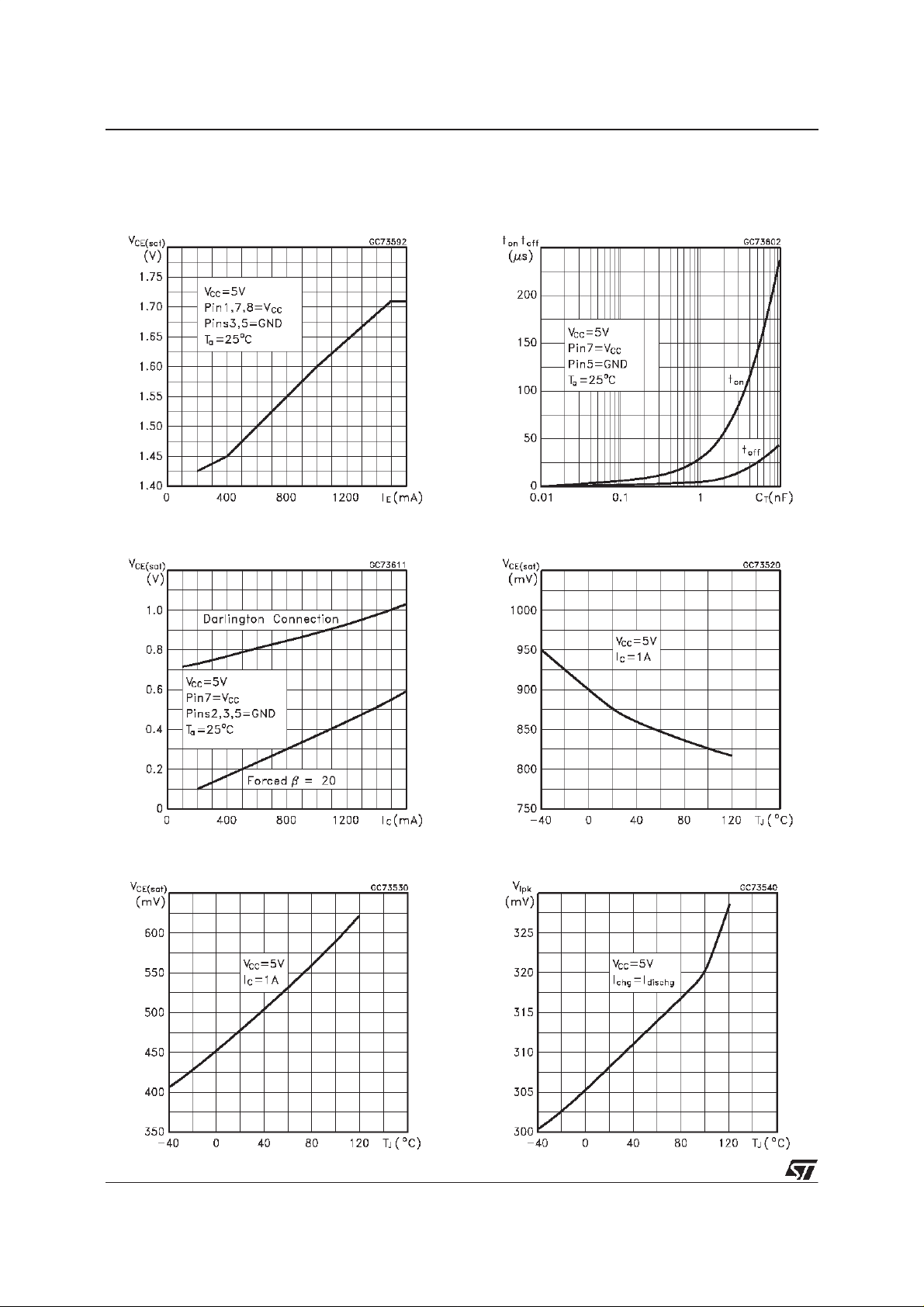
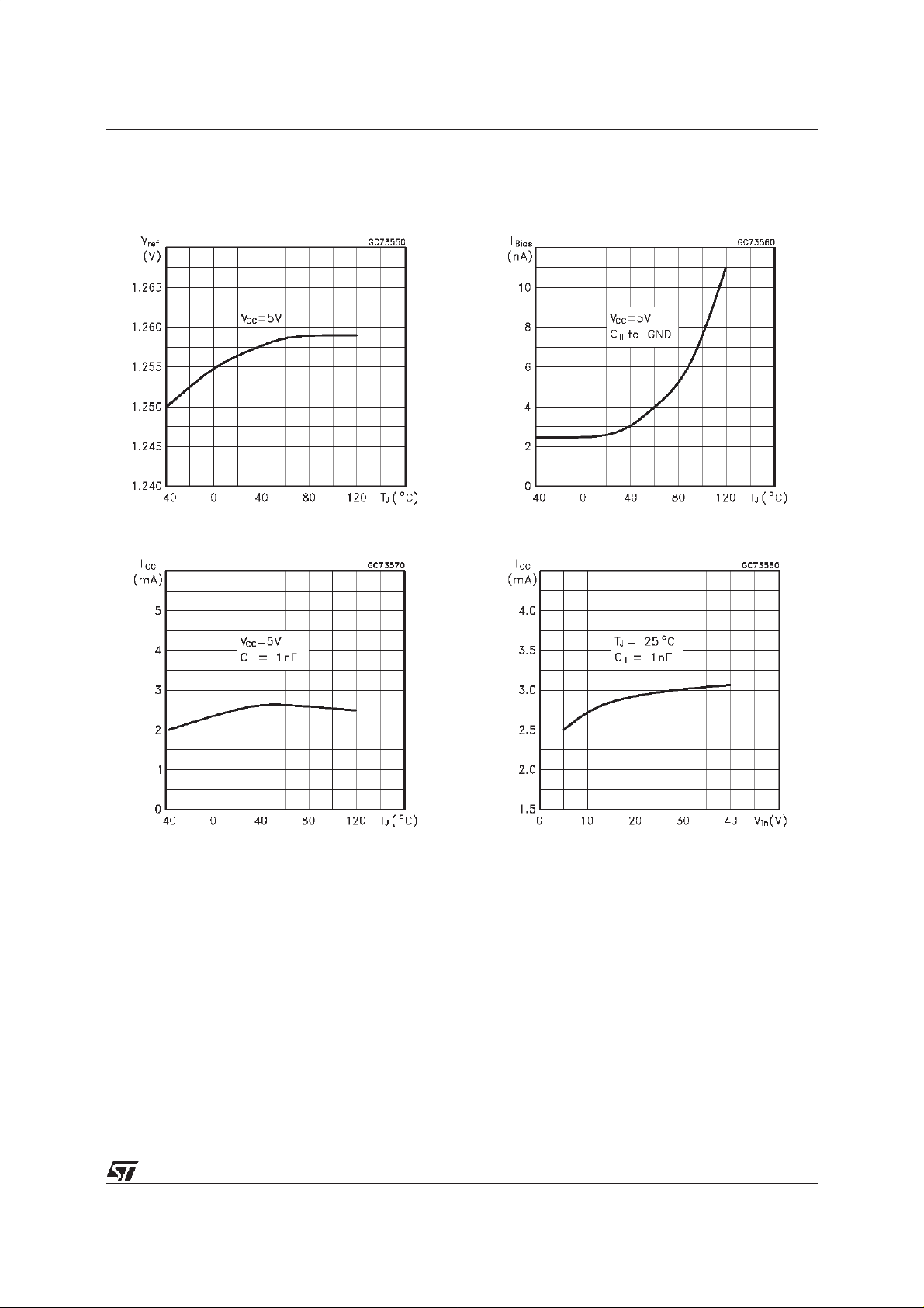
TYPICALELECTRICAL CHARACTERISTICS
EmitterFollowerConfigurationOutput Saturation
Voltagevs EmitterCurrent
CommonEmitterConfiguration Output Switch
SaturationVoltage vs CollectorCurrent
OutputSwitchON-OFF Timevs Oscillator
TimingCapacitor
DarlingtonConfiguration CollectorEmitter
SaturationVoltage (V
) vsTemperature
CE(sat)
PowerCollectorEmitter Saturation Voltage
(V
4/15
) vsTemperature
CE(sat)
CurrentLimit Sense VoltageVoltage(V
Temperature
ipk
)vs
Page 5
MC34063A
TYPICALELECTRICAL CHARACTERISTICS
(Continued)
ReferenceVoltagevs Temperature BiasCurrent vsTemperature
SupplyCurrent vs Temperature SupplyCurrent vs Input Voltage
5/15
Page 6
MC34063A
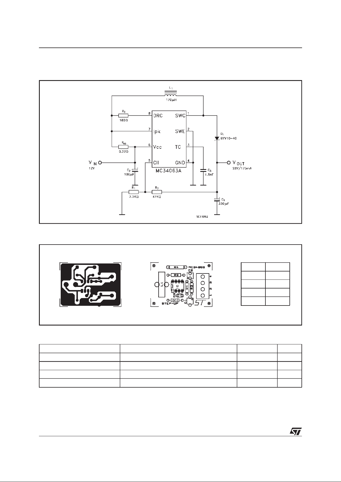
TYPICALAPPLICATION CIRCUIT
Step-UpConverter
PrintedDemoboard
TestCondition (V
Test Conditions Value (Typ.) Unit
LineRegulation V
LoadRegulation V
OutputRipple V
Efficency V
OUT
= 28V)
Symbol Pin
Vout 1
GND 2
GND 3
Vin 4
=8 to 16V, IO=175mA 30 mV
IN
=12V, IO=75 to 175mA 10 mV
IN
=12V, IO=175mA 300 mV
IN
=12V, IO=175mA 89 %
IN
6/15
Page 7

Step-DownConverter
MC34063A
PrintedDemoboard
TestCondition (V
Test Conditions Value (Typ.) Unit
LineRegulation V
LoadRegulation V
OutputRipple V
Efficency V
I
SC
OUT
= 5V)
Symbol Pin
Vout 1
GND 2
GND 3
Vin 4
=15 to 25V, IO= 500mA 5 mV
IN
=25V, IO=50 to 500mA 30 mV
IN
=25V, IO=500mA 100 mV
IN
=25V, IO=500mA 80 %
IN
VIN=25V, R
LOAD
= 0.1
Ω
1.2 A
7/15
Page 8
MC34063A
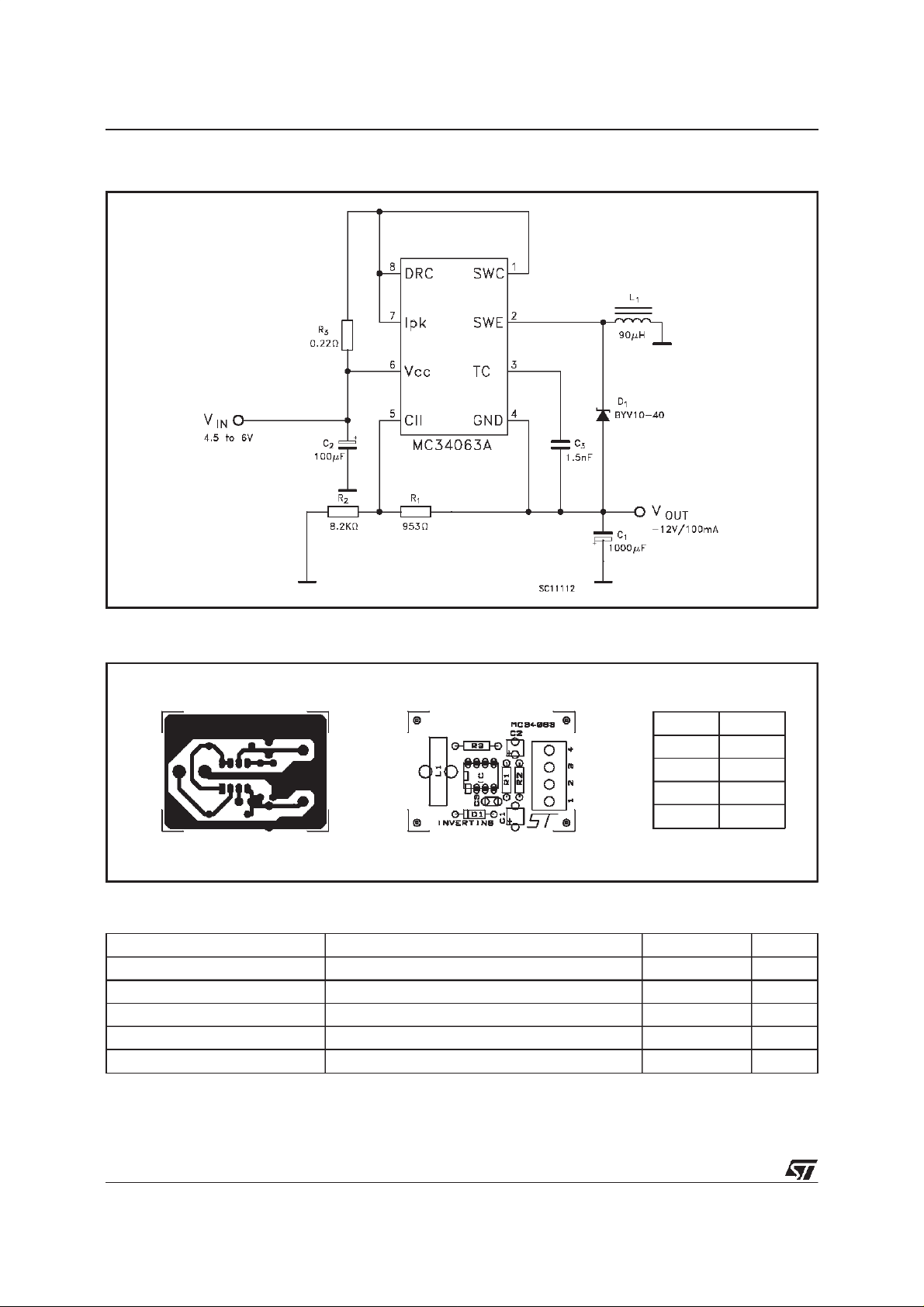
VoltageInvertingConverter
PrintedDemoboard
TestCondition (V
Test Conditions Value (Typ.) Unit
LineRegulation V
LoadRegulation V
OutputRipple V
Efficency V
I
SC
OUT
=-12V)
Symbol Pin
Vout 1
GND 2
GND 3
Vin 4
=4.5 to 6V, IO=100mA 15 mV
IN
=5V, IO=10to 100mA 20 mV
IN
=5V, IO=100mA 230 mV
IN
=5V, IO=100mA 58 %
IN
VIN=5V, R
lLOAD
= 0.1
Ω
0.9 A
8/15
Page 9

Calculation
MC34063A
Parameter Step-Up
(Discontinuos mode)
t
on/toff
(ton+t
)max 1/f
off
C
T
I
PK(switch)
R
SC
C
O
L(min) V
NOTES:
V
= Saturation voltage of the output switch
sat
V
= Foward voltage drop ofthe output rectifier
F
THE FOLLOWING POWER SUPPLY CHARACTERISTICS MUST BECHOSEN:
V
= Nominal input voltage
in
= Desired output voltage,|V
V
out
= Desired output current
I
out
= Minimum desired output switching frequency at the selected values ofVin and Io
f
min
V
= Desired peak to peak output ripple voltage. In practice, the calculaed capacitor value will and to be increased due to its equivalent
ripple
series resistance and board layout. The ripplevoltage should be kept to a low value since it will directly affect the line and load regulation.
out
V
out+VF−Vin(min)
V
in(min)
4.5x 10⁻⁵t
2I
out(max)
0.3/ I
≅
V
in(mi n)−Vsat
I
PK (switch)
| = 1.25(1+R2/R1)
− V
min
[(ton/t
PK(switch)
I
outton
ripple(p−p
t
on(max)
sat
on
)+1] 2I
off
)
Step-Down
(Continuos mode)
V
out+VF
V
− V
in(min)
1/f
min
4.5x 10⁻⁵t
out(max)
0.3/I
PK(switch)
I
PK(switch)(ton+toff
8V
ripple
V
− V
in(min)
sat−Vout
I
PK (switch)
sat
p−p)
(
− V
on
out
)
t
on (max)
Voltage Inverting
(Discontinuos mode)
|V
| + V
out
F
Vin− V
sat
1/f
min
2I
out(max)
V
in(min)
I
PK (switch)
4.5x1 0-5t
0.3/I
≅
[(ton/t
PK(switch )
I
outton
V
ripple(p−p
− V
sat
on
)+1]
off
)
t
on (max)
Step-upWith External NPN Switch
9/15
Page 10
MC34063A
Step-downWithExternal NPN Switch
Step-downWithExternal PNP Switch
10/15
Page 11
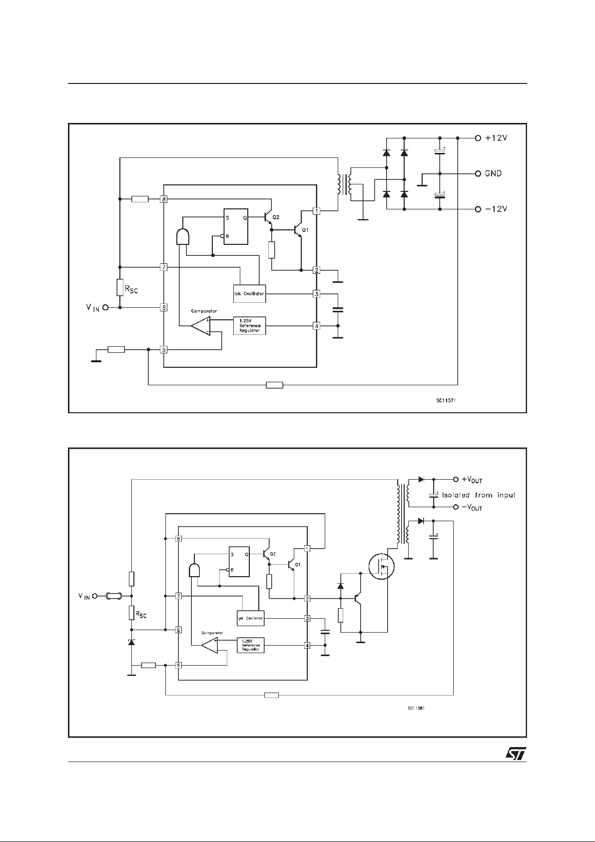
VoltageInvertingWith ExternalNPN Switch
MC34063A
VoltageInvertingWith ExternalPNP SaturatedSwitch
11/15
Page 12
MC34063A
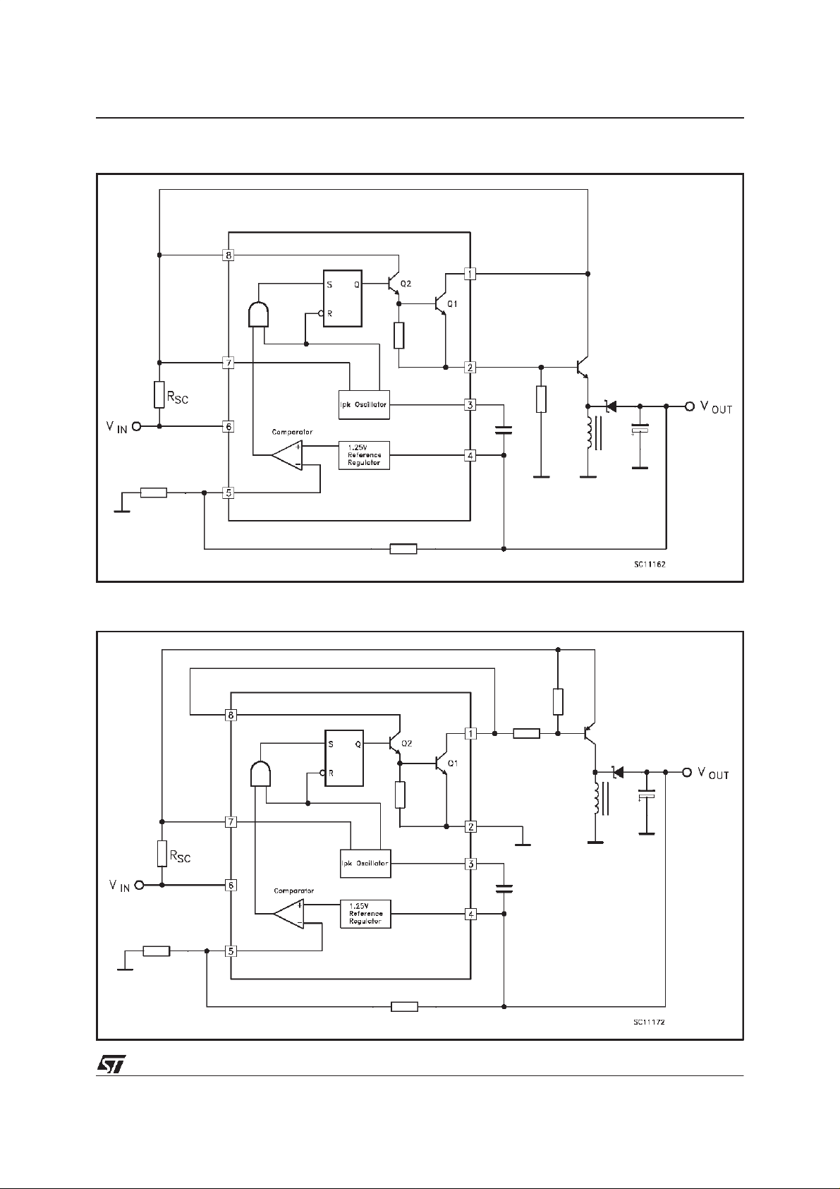
DualOutput Voltage
HigherOutputPower, HigherInput Voltage
12/15
Page 13

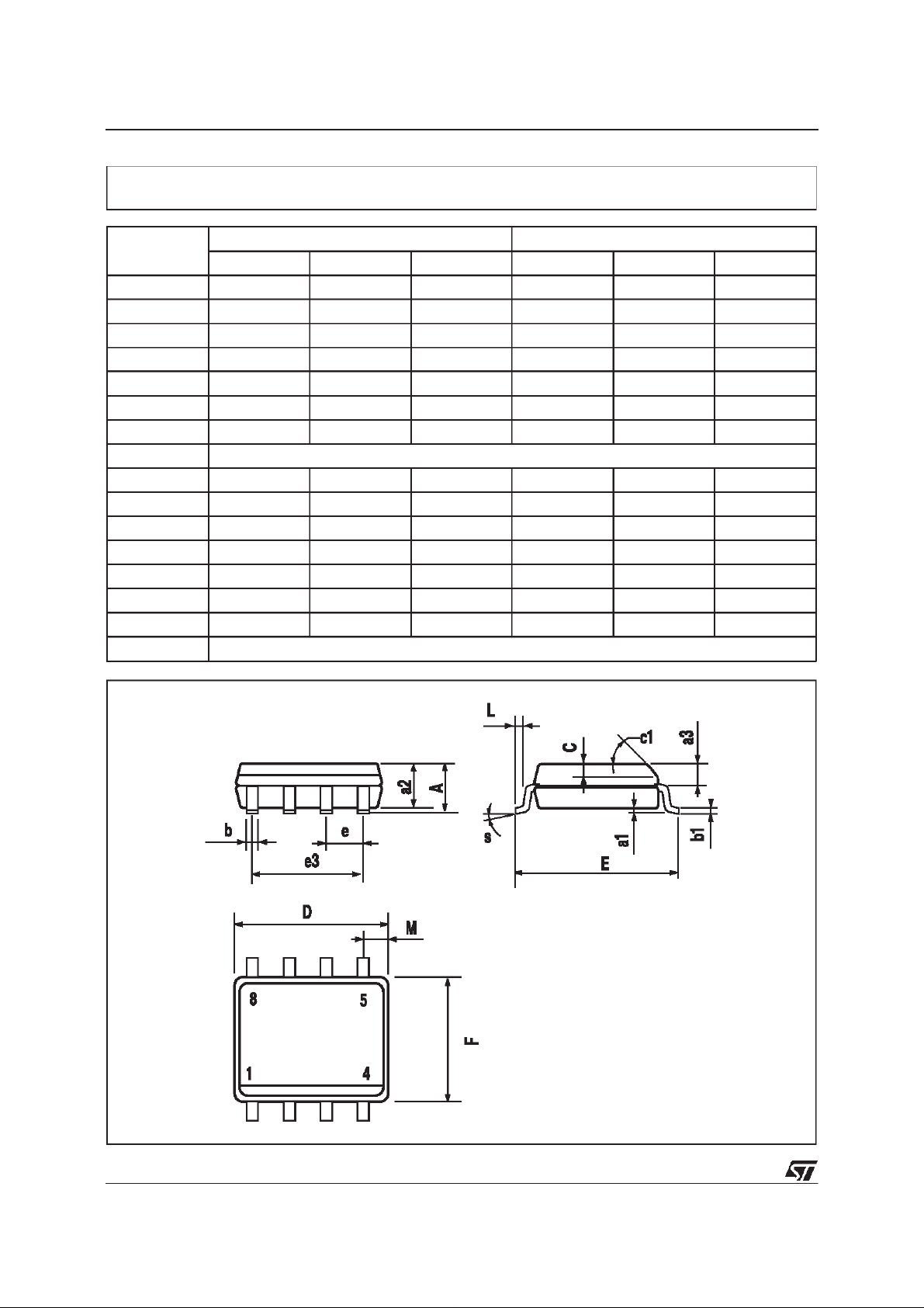
Plastic DIP-8 MECHANICALDATA
MC34063A
DIM.
MIN. TYP. MAX. MIN. TYP. MAX.
A 3.3 0.130
a1 0.7 0.028
B 1.39 1.65 0.055 0.065
B1 0.91 1.04 0.036 0.041
b 0.5 0.020
b1 0.38 0.5 0.015 0.020
D 9.8 0.386
E 8.8 0.346
e 2.54 0.100
e3 7.62 0.300
e4 7.62 0.300
F 7.1 0.280
I 4.8 0.189
L 3.3 0.130
Z 0.44 1.6 0.017 0.063
mm inch
P001F
13/15
Page 14
MC34063A
SO-8 MECHANICAL DATA
DIM.
MIN. TYP. MAX. MIN. TYP. MAX.
A 1.75 0.068
a1 0.1 0.25 0.003 0.009
a2 1.65 0.064
a3 0.65 0.85 0.025 0.033
b 0.35 0.48 0.013 0.018
b1 0.19 0.25 0.007 0.010
C 0.25 0.5 0.010 0.019
c1 45 (typ.)
D 4.8 5.0 0.188 0.196
E 5.8 6.2 0.228 0.244
e 1.27 0.050
e3 3.81 0.150
F 3.8 4.0 0.14 0.157
L 0.4 1.27 0.015 0.050
M 0.6 0.023
S 8 (max.)
mm inch
14/15
0016023
Page 15

MC34063A
Information furnished is believed to be accurate and reliable. However, STMicroelectronics assumes no responsibility for the consequences
of use of such information nor for any infringement of patents or other rights of third parties which may result from its use. No license is
granted by implication or otherwise under any patent or patent rights of STMicroelectronics. Specification mentioned in this publication are
subject tochange without notice. Thispublication supersedes andreplaces allinformation previously supplied. STMicroelectronics products
are not authorized for use as critical components in life support devices or systems withoutexpress written approval of STMicroelectronics.
The ST logo isa registeredtrademark of STMicroelectronics
2000 STMicroelectronics – Printedin Italy– All RightsReserved
STMicroelectronics GROUP OF COMPANIES
Australia - Brazil- China - Finland - France - Germany - Hong Kong - India- Italy - Japan - Malaysia - Malta - Morocco
Singapore - Spain- Sweden- Switzerland- UnitedKingdom - U.S.A.
http://www.st.com
.
15/15
 Loading...