

Page 1
Order this document by MC34060A/D
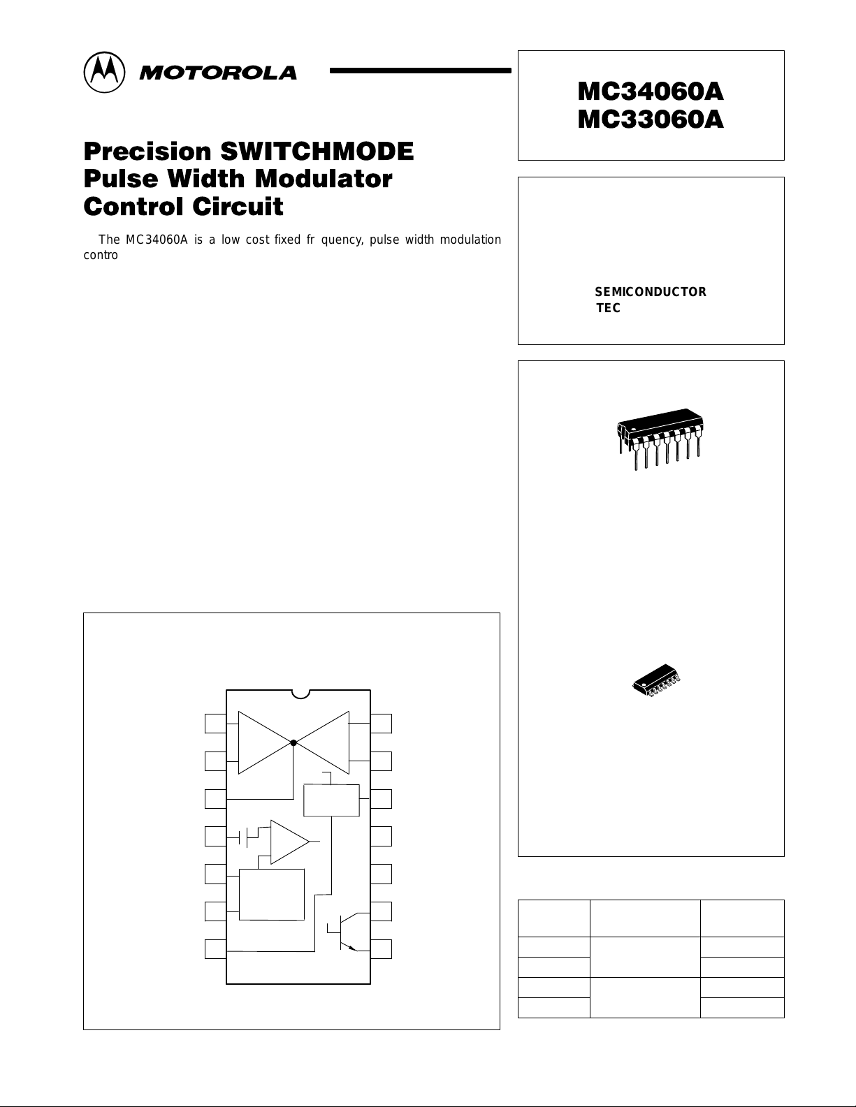
The MC34060A is a low cost fixed frequency, pulse width modulation
control circuit designed primarily for single–ended SWITCHMODE power
supply control.
The MC34060A is specified over the commercial operating temperature
range of 0° to +70°C, and the MC33060A is specified over an automotive
temperature range of –40° to +85°C.
• Complete Pulse Width Modulation Control Circuitry
• On–Chip Oscillator with Master or Slave Operation
• On–Chip Error Amplifiers
• On–Chip 5.0 V Reference, 1.5% Accuracy
• Adjustable Dead–Time Control
• Uncommitted Output Transistor Rated to 200 mA Source or Sink
• Undervoltage Lockout
PRECISION SWITCHMODE
PULSE WIDTH MODULATOR
CONTROL CIRCUIT
SEMICONDUCTOR
TECHNICAL DATA
14
1
P SUFFIX
PLASTIC PACKAGE
CASE 646
PIN CONNECTIONS
Noninv
Input
Inv
Input
Compen/PWM
Comp Input
Dead–Time
Control
C
T
R
T
Ground
+
1
Error
12
Amp
–
2
3
0.1V
4
5
Oscillator
6
78
V
CC
(Top View)
MOTOROLA ANALOG IC DEVICE DATA
Error
Amp
5.0 V
ref
+
–
Q1
Noninv
14
Input
Inv
13
Input
V
12
ref
N.C.
11
V
10
CC
C
9
E
14
1
D SUFFIX
PLASTIC PACKAGE
CASE 751A
(SO–14)
ORDERING INFORMATION
Operating
Device
MC34060AD
MC34060AP
MC33060AD
MC33060AP
Motorola, Inc. 1996 Rev 1
Temperature Range
TA = 0° to +70°C
TA = – 40° to +85°C
Package
SO–14
Plastic DIP
SO–14
Plastic DIP
1
Page 2
MC34060A MC33060A
MAXIMUM RATINGS
noted.)
Power Supply Voltage V
Collector Output Voltage V
Collector Output Current (Note 1) I
Amplifier Input Voltage Range V
Power Dissipation @ TA ≤ 45°C P
Operating Junction Temperature T
Storage Temperature Range T
Operating Ambient Temperature Range
For MC34060A
For MC33060A
NOTES: 1. Maximum thermal limits must be observed.
(Full operating ambient temperature range applies, unless otherwise
Rating
THERMAL CHARACTERISTICS
Characteristics Symbol
Thermal Resistance, Junction–to–Ambient R
Derating Ambient Temperature T
θJA
A
Symbol Value Unit
CC
stg
T
C
C
in
D
J
A
P Suffix
Package
42 V
42 V
500 mA
–0.3 to +42 V
1000 mW
125 °C
–55 to +125 °C
0 to +70
–40 to +85
D Suffix
Package
80 120 °C/W
45 45 °C
°C
Unit
RECOMMENDED OPERATING CONDITIONS
Condition/Value Symbol Min Typ Max Unit
Power Supply Voltage V
Collector Output Voltage V
Collector Output Current I
Amplifier Input Voltage V
Current Into Feedback Terminal I
Reference Output Current I
Timing Resistor R
Timing Capacitor C
Oscillator Frequency f
PWM Input Voltage (Pins 3 and 4) – –0.3 – 5.3 V
ELECTRICAL CHARACTERISTICS (V
for min/max values TA is the operating ambient temperature range that applies, unless otherwise noted.)
Characteristics
REFERENCE SECTION
Reference Voltage (IO = 1.0 mA, TA 25°C)
TA = T
TA = T
Line Regulation
(VCC = 7.0 V to 40 V, IO = 10 mA))
Load Regulation
(IO = 1.0 mA to 10 mA)
Short Circuit Output Current
(V
ref
low
low
= 0 V)
to T
to T
– MC34060A
high
– MC33060A
high
= 15 V, CT = 0.01 µF, RT = 12 kΩ, unless otherwise noted. For typical values TA = 25°C,
CC
CC
C
C
in
fb
ref
T
T
osc
Symbol Min Typ Max Unit
V
ref
Reg
line
Reg
load
I
SC
7.0 15 40 V
– 30 40 V
– – 200 mA
–0.3 – VCC –2 V
– – 0.3 mA
– – 10 mA
1.8 47 500 kΩ
0.00047 0.001 10 µF
1.0 25 200 kHz
4.925
4.9
4.85
– 2.0 25 mV
– 2.0 15 mV
15 35 75 mA
5.0
–
–
5.075
5.1
5.1
V
2
MOTOROLA ANALOG IC DEVICE DATA
Page 3
MC34060A MC33060A
ELECTRICAL CHARACTERISTICS (V
= 15 V, CT = 0.01 µF, RT = 12 kΩ, unless otherwise noted. For typical values TA = 25°C,
CC
for min/max values TA is the operating ambient temperature range that applies, unless otherwise noted.)
Characteristics
Symbol Min Typ Max Unit
OUTPUT SECTION
Collector Off–State Current
(VCC = 40 V, VCE = 40 V)
Emitter Off–State Current
(VCC = 40 V, VCE = 40 V, VE = 0 V)
Collector–Emitter Saturation Voltage (Note 2)
Common–Emitter
I
C(off)
I
) – – –100 µA
E(off
V
sat(C)
– 2.0 100 µA
–
1.1
(VE = 0 V, IC = 200 mA)
Emitter–Follower
(VC = 15 V, IE = –200 mA)
Output Voltage Rise T ime (TA = 25°C)
Common–Emitter (See Figure 12)
Emitter–Follower (See Figure 13)
Output Voltage Fall T ime (TA = 25°C)
Common–Emitter (See Figure 12
Emitter–Follower (See Figure 13)
V
sat(E)
–
t
r
–
–
t
r
–
–
1.5
100
100
40
40
ERROR AMPLIFIER SECTION
Input Offset Voltage
(V
O[Pin 3]
= 2.5 V)
Input Offset Current
(V
C[Pin 3]
= 2.5 V)
Input Bias current
(V
O[Pin 3]
= 2.5 V)
Input Common Mode Voltage Range
(VCC = 40 V)
Inverting Input Voltage Range V
Open–Loop Voltage Gain
(∆VO = 3.0 V, VO = 0.5 V to 3.5 V, RL = 2.0 kΩ)
Unity–Gain Crossover Frequency
(VO = 0.5 V to 3.5 V, RL = 2.0 kΩ)
Phase Margin at Unity–Gain
(VO = 0.5 V to 3.5 V, RL = 2.0 kΩ)
Common Mode Rejection Ratio
V
IO
I
IO
I
IB
V
ICR
IR(INV)
A
VOL
f
c
φ
m
– 2.0 10 mV
– 5.0 250 nA
– –0.1 –2.0 µA
0 to
– – V
VCC –2.0
–0.3 to
– – V
VCC–2.0
70 95 – dB
– 600 – kHz
– 65 – deg.
CMRR 65 90 – dB
(VCC = 40 V, Vin = 0 V to 38 V))
Power Supply Rejection Ratio
PSRR – 100 – dB
(∆VCC = 33 V, VO = 2.5 V, RL = 2.0 kΩ)
Output Sink Current
(V
O[Pin 3]
= 0.7 V)
Output Source Current
(V
NOTES: 2. Low duty cycle techniques are used during test to maintain junction temperature as close to ambient temperatures as possible.
O[Pin 3]
T
low
T
low
= 3.5 V)
= –40°C for MC33060A T
= 0°C for MC34060A T
= +85°C for MC33060A
high
= +70°Cfor MC34060A
high
IO– 0.3 0.7 – mA
IO+ –2.0 –4.0 – mA
1.5
2.5
200
200
100
100
V
ns
ns
MOTOROLA ANALOG IC DEVICE DATA
3
Page 4
MC34060A MC33060A
ELECTRICAL CHARACTERISTICS
for min/max values TA is the operating ambient temperature range that applies, unless otherwise noted.)
Characteristics
PWM COMPARATOR SECTION (Test circuit Figure 11)
Input Threshold Voltage
(Zero Duty Cycle)
Input Sink Current
(V
= 0.7 V)
[Pin 3]
DEAD–TIME CONTROL SECTION (Test circuit Figure 11)
Input Bias Current (Pin 4)
(Vin = 0 V to 5.25 V)
Maximum Output Duty Cycle
(Vin = 0 V, CT = 0.01 µF, RT = 12 kΩ)
(Vin = 0 V, CT = 0.001 µF, RT = 47 kΩ)
Input Threshold Voltage (Pin 4)
(Zero Duty Cycle)
(Maximum Duty Cycle)
OSCILLATOR SECTION
Frequency
(CT = 0.01 µF, RT = 12 kΩ, TA = 25°C)
TA = T
TA = T
(CT = 0.001 µF, RT = 47 kΩ)
Standard Deviation of Frequency*
(CT = 0.001 µF, RT = 47 kΩ)
Frequency Change with Voltage
(VCC = 7.0 V to 40 V)
Frequency Change with Temperature
(∆TA =T
(CT = 0.01 µF, RT = 12 kΩ)
UNDERVOLTAGE LOCKOUT SECTION
Turn–On Threshold (VCC increasing, I
Hysteresis V
TOTAL DEVICE
Standby Supply Current
(Pin 6 at V
(VCC = 15 V)
(VCC = 40 V)
Average Supply Current
(V
[Pin 4]
*Standard deviation is a measure of the statistical distribution about the mean as derived from the formula; σ =
to T
low
to T
low
to T
low
ref
= 2.0 V, CT = 0.001 µF, RT = 47 kΩ). See Figure 11.
– MC34060A
high
– MC33060A
high
)
high
, all other inputs and outputs open)
(VCC = 15 V, CT = 0.01 µF, RT = 12 kΩ, unless otherwise noted. For typical values TA = 25°C,
Symbol Min Typ Max Unit
= 1.0 mA) V
ref
V
TH
I
I
I
IB(DT)
DC
max
V
TH
f
osc
σf
osc
∆f
(∆V) – 0.5 2.0 %
osc
∆f
(∆T)
osc
th
H
I
CC
I
S
– 3.5 4.5 V
0.3 0.7 – mA
– –1.0 –10 µA
90
–
–
0
9.7
9.5
9.0
–
– 1.5 – %
–
–
4.0 4.7 5.5 V
50 150 300 mV
–
–
– 7.0 – mA
96
92
2.8
–
10.5
–
–
25
4.0
–
5.5
7.0
11.3
11.5
11.5
N
Σ (xn –x)
n – 1
N–1
100
%
–
V
3.3
–
kHz
–
%
–
–
mA
10
15
2
4
MOTOROLA ANALOG IC DEVICE DATA
Page 5
MC34060A MC33060A
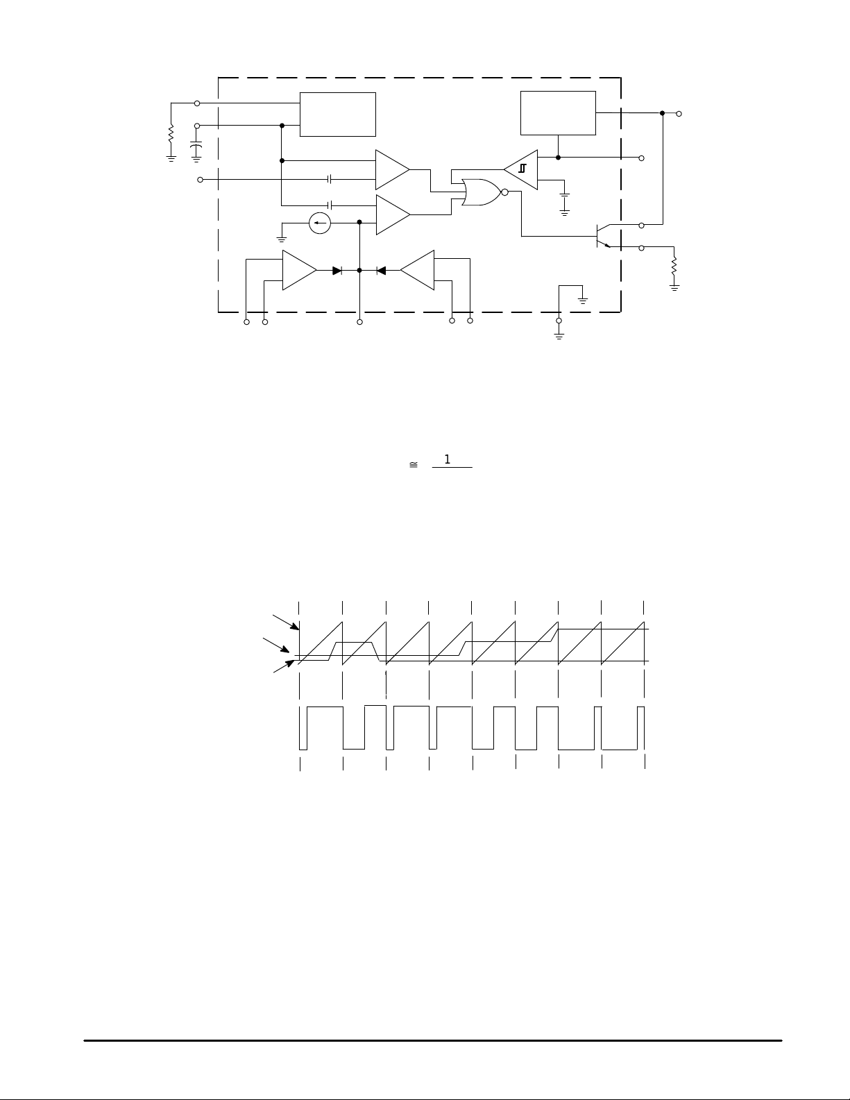
Figure 1. Block Diagram
R
T
C
T
Dead–Time
Control
6
5
4
12 3
Error Amp
1
Oscillator
0.12V
0.7V
≈
0.7mA
++
1
––
Feedback/PWM
Comparator Input
This device contains 46 active transistors.
Dead–Time
Comparator
–
+
–
+
PWM.
Comparator
2
Undervoltage
Lockout
13 14
Error Amp
2
Reference
Regulator
–
+
7 Gnd
10
12
V
TH
9
Q1
8
V
CC
Ref Out
Collector
Emitter
Description
The MC34060A is a fixed–frequency pulse width modulation control circuit, incorporating the primary building blocks required
for the control of a switching power supply (see Figure 1). An internal–linear sawtooth oscillator is frequency–programmable by
two external components, RT and CT. The approximate oscillator frequency is determined by:
^
1.2
RT • C
T
f
osc
For more information refer to Figure 3.
Output pulse width modulation is accomplished by comparison of the positive sawtooth waveform across capacitor CT to either
of two control signals. The output is enabled only during that portion of time when the sawtooth voltage is greater than the control
signals. Therefore, an increase in control–signal amplitude causes a corresponding linear decrease of output pulse width. (Refer
to the Timing Diagram shown in Figure 2.)
Figure 2. Timing Diagram
Capacitor C
Feedback/P.W.M.
Comparator
Dead–Time Control
T
Output Q1,
Emitter
APPLICATIONS INFORMATION
The control signals are external inputs that can be fed into
the dead–time control, the error amplifier inputs, or the
feed–back input. The dead–time control comparator has an
effective 120 mV input offset which limits the minimum output
dead time to approximately the first 4% of the sawtooth–cycle
time. This would result in a maximum duty cycle of 96%.
Additional dead time may be imposed on the output by setting
the dead time–control input to a fixed voltage, ranging
between 0 V to 3.3 V.
The pulse width modulator comparator provides a means
for the error amplifiers to adjust the output pulse width from
the maximum percent on–time, established by the dead time
control input, down to zero, as the voltage at the feedback pin
varies from 0.5 V to 3.5 V. Both error amplifiers have a
common mode input range from –0.3 V to (VCC –2.0 V), and
may be used to sense power supply output voltage and
current. The error–amplifier outputs are active high and are
ORed together at the noninverting input of the pulse–width
modulator comparator. With this configuration, the amplifier
that demands minimum output on time, dominates control of
the loop.
The MC34060A has an internal 5.0 V reference capable of
sourcing up to 10 mA of load currents for external bias
circuits. The reference has an internal accuracy of ±5% with a
typical thermal drift of less than 50 mV over an operating
temperature range of 0° to +70°C.
MOTOROLA ANALOG IC DEVICE DATA
5
Page 6

MC34060A MC33060A
Figure 3. Oscillator Frequency
versus Timing Resistance
500 k
VCC = 15 V
0.001
µ
CT = 0.01 µF
1.0 µF
F
Ω
)
100 k
10 k
, OSCILLAT OR FREQUENCY (Hz)
1.0 k
osc
f
500
1.0 k 2.0 k 5.0 k 10 k 20 k 50 k 100 k 200 k 500 k
RT, TIMING RESISTANCE (
Figure 5. Percent Deadtime versus
Oscillator Frequency
20
18
16
14
12
10
8.0
6.0
4.0
2.0
% DT, PERCENT DEAD-TIME, Q1 OUTPUT
0
500 10 k 100 k 500 k
1.0 k
f
, OSCILLAT OR FREQUENCY (Hz)
osc
0.01 µF
CT = 0.001 µF
1.0 M
Figure 4. Open Loop V oltage Gain and Phase
versus Frequency
120
110
100
90
80
70
60
50
40
30
, OPEN LOOP VOL TAGE GAIN (dB)
20
VOL
10
A
0
1.0 10 100 1.0 k 10 k 100 k 1.0 M
A
VOL
f, FREQUENCY (Hz)
VCC = 15 V
∆
VO = 3.0 V
RL = 2.0 k
θ
Figure 6. Percent Duty Cycle versus
Dead–Time Control Voltage
100
80
60
40
20
PERCENT DUTY CYCLE (%)
0
0 1.0 2.0 3.0 3.5
DEAD–TIME CONTROL VOLTAGE (V)
VCC = 15 V
CT = 0.001
RT = 47 k
Ω
0
–20
–40
–60
–80
–100
–120
, EXCESS PHASE (DEGREES)
–140
θ
–160
–180
Figure 7. Emitter–Follower Configuration
Output Saturation Voltage versus
Emitter Current
1.9
1.8
1.7
1.6
1.5
1.4
, SATURATION VOLTAGE (V)
1.3
1.2
CE(SAT)
V
1.1
0 100 200 300 400 500
IE, EMITTER CURRENT (mA)
6
Figure 8. Common–Emitter Configuration
Output Saturation Voltage versus
Collector Current
2.0
1.8
1.6
1.4
1.2
1.0
, SATURATION VOLTAGE (V)
0.8
0.6
CE(SAT)
V
0.4
0 100 200 300 400 500
IC, COLLECTOR CURRENT (mA)
MOTOROLA ANALOG IC DEVICE DATA
Page 7

MC34060A MC33060A
Figure 9. Standby Supply Current
versus Supply V oltage
10
9.0
8.0
7.0
6.0
5.0
4.0
3.0
, SUPPLY CURRENT (mA)
2.0
CC
I
1.0
0
0 5.0 10 15 20 25 30 35 40
VCC, SUPPLY VOLTAGE (V)
Figure 10. Undervoltage Lockout Thresholds
versus Reference Load Current
6.0
5.5
5.0
4.5
4.0
, UNDERVOL TAGE LOCKOUT THRESHOLD (V)
0 5.0 10 15 20 25 30 35 40
TH
V
Turn On
Turn Off
IL, REFERENCE LOAD CURRENT (mA)
Figure 11. Error Amplifier Characteristics Figure 12. Deadtime and Feedback Control
Error Amplifier
+
Under Test
V
in
V
ref
–
+
–
Feedback
Terminal
(Pin 3)
Other Error
Amplifier
T est
Inputs
50k
Ω
VCC = 15V
Dead–
Time
Feedback
R
T
C
T
(+)
(–)
Error
(+)
(–)
V
CC
Gnd
C
E
Ref
Out
150
2W
Ω
Output
Figure 13. Common–Emitter Configuration
and Waveform
15V
R
L
Ω
68
C
Output
Transistor
90% 90%
V
C
10% 10%
t
r
CL
15pF
E
t
f
MOTOROLA ANALOG IC DEVICE DATA
Figure 14. Emitter–Follower Configuration
and Waveform
15V
C
V
C
Output
Transistor
V
E
R
L
68
Ω
90% 90%
10% 10%
t
r
CL
15pF
t
f
E
V
E
7
Page 8

MC34060A MC33060A
Figure 15. Error Amplifier Sensing Techniques
V
O
To Output
Voltage of
System
R
1
1
V
ref
R
2
2
+
–
Error
Amp
Positive Output Voltage
R
(1 +
1
)
R
2
VO = V
ref
3
3
Error
Amp
Negative Output Voltage
VO = –V
ref
+
–
(1 +
1
2
R
1
)
R
2
Figure 16. Deadtime Control Circuit Figure 17. Soft–Start Circuit
V
ref
R
2
R
1
To Output
Voltage of
System
V
O
Output
V
ref
Q
R
T
65
47k
0.001
D
C
T
R
1
4
T
Max % On Time
R
2
160
1 +
R
1
R
2
≈
92 –
Output Q
Figure 18. Slaving Two or More Control Circuits
V
ref
6
R
T
Master
5
C
T
C
R
T
T
V
ref
+
C
V
ref
D
T
R
4
R
S
1
–
2
6
R
T
Slave
5
C
T
8
(Additional
Circuits)
MOTOROLA ANALOG IC DEVICE DATA
Page 9

Vin = 8.0V to 40V
+
50/50
47k
0.01
MC34060A MC33060A
Figure 19. Step–Down Converter with Soft–Start
and Output Current Limiting
Tip 32
47
4.7k
10
V
CC
MC34060A
DTCTR
56
4
0.001
Gnd
T
47k
9
C
8
E
7
1.0M
4.7k
0.01
4.7k
1
2
3
14
13
12
10/16V
+
4.7k
+
–
Comp
+
–
V
ref
75
150
MR850
µ
H @ 2.0A
+
1000
6.3V
V
out
5.0V/1.0A
150
Test Conditions Results
Line Regulation Vin = 8.0 V to 40 V, IO = 1.0 A 25 mV 0.5%
Load Regulation Vin = 12 V, IO = 1.0 mA to 1.0 A 3.0 mV 0.06%
Output Ripple Vin = 12 V, IO = 1.0 A 75 mV p–p P.A.R.D.
Short Circuit Current Vin = 12 V, RL = 0.1 Ω 1.6 A
Efficiency Vin = 12 V, IO = 1.0 A 73%
390
0.1
MOTOROLA ANALOG IC DEVICE DATA
9
Page 10

Vin = 8.0V to 26V
4.7k
50/35V
33k
2.7M
0.05
3.9k
22k
MC34060A MC33060A
Figure 20. Step–Up Converter
10
V
CC
MC34060A
DTCTR
4
5
0.001
9
C
8
E
7
Gnd
T
6
47k
14
13
12
1
2
3
4.7k
+
–
Comp
+
–
V
ref
390
150
µ
470
H @ 4.0A
300
0.1
MR850
Tip 111
20
µ
H @ 1.0A
*
++
470/35V 470/35V
+
V
out
28V/
0.5A
*
Test Conditions Results
Line Regulation Vin = 8.0 V to 26 V, IO = 0.5 A 40 mV 0.14%
Load Regulation Vin = 12 V, IO = 1.0 mA to 0.5 A 5.0 mV 0.18%
Output Ripple Vin = 12 V, IO = 0.5 A 24 mV p–p P.A.R.D.
Efficiency Vin = 12 V, IO = 0.5 A 75%
*Optional circuit to minimize output ripple
10
MOTOROLA ANALOG IC DEVICE DATA
Page 11

MC34060A MC33060A
Figure 21. Step–Up/Down Voltage Inverting Converter
with Soft–Start and Current Limiting
Vin = 8.0V to 40V
7.5k
+
50/50V
0.01
3.3k
47k
1.0M
0.01
10k
47k
30k
1
2
3
14
13
12
10/16V
4.7k
Tip 32C
47
10
V
CC
+
–
Comp
MC34060A 330/16V
+
–
V
ref
DTCTR
4
56
0.001
820
C
E
Gnd
T
47k
75
9
8
7
MR851
µ
H
150
@ 2.0A
+
330/16V
20
µ
H *
@ 1.0A
*
+
V
out
–15V/
0.25A
Test Conditions Results
Line Regulation Vin = 8.0 V to 40 V, IO = 250 mA 52 mV 0.35%
Load Regulation Vin = 12 V, IO = 1.0 to 250 mA 47 mV 0.32%
Output Ripple Vin = 12 V, IO = 250 mA 10 mV p–p P.A.R.D.
Short Circuit Current Vin = 12 V, RL = 0.1 Ω 330 mA
Efficiency Vin = 12 V, IO = 250 mA 86%
*Optional circuit to minimize output ripple
1.0
MOTOROLA ANALOG IC DEVICE DATA
11
Page 12

5.0V/3.0A
1
L
MC34060A MC33060A
Figure 22. 33 W Off–Line Flyback Converter with Soft–Start and Primary Power Limiting
12/075A
+
100/10V
+
Common
+
2
L
10/35V
+
10/35V
+
3
L
+
–12/0.75A
1N5824
2
T
1N4934
2200/10V
1N4934
1000/25V
+
47/25V
22k
1000/25V
9
CC
V
10
1
1N4934
1N4937
C
+
2
0.025 gap in each leg.″
Primary, 2 each, 75 turns #25 Awg Bifilar wound
Feedback: 15 turns #26 Awg
Secondary, 5.0 V, 6 turns @33 Awg Bifilar wound
10
47k
1.5k
27k
Secondary, 2 each, 14 turns #24 Awg Bifilar wound
1.0
11k
L1 – Coilcraft Z7156, 15 H @ 5.0 Aµ
L2, L3 – Coilcraft Z7157, 25 H @ 1.0 Aµ
2.7k
1N4148
20 mV 0.40%
52 mV 0.26%
= 3.0 A
= ±0.75 A
O
O
= 95 Vac to 135 Vac, I
= 95 Vac to 135 Vac, I
in
in
V
V
476 mV 9.5%
= 1.0 A to 4.0 A
O
= 115 Vac, I
in
V
300 mV 2.5%
= ±0.4 A to±0.9 A
O
= 115 Vac, I
in
V
45 mV p–p P.A.R.D.
75 mV p–p P.A.R.D.
= 3.0 A
= ±0.75 A
O
O
= 115 Vac, I
= 115 Vac, I
in
in
V
V
74%
5.0 V = 3.0 A
O
= 115 Vac, I
in
V
±12 V = ±0.75 A
O
I
T1 – Coilcraft W2961
T2 – Core: Coilcraft 11–464–16,
Bobbin: Coilcraft 37–573
Windings:
MJE
13005
A55
MPS
+
A05
10/25V
MPS
200 47
7
8
E
Gnd
T
R
T
12
C
T
D
ref
V
8.2k
0.001
456
+
MC34060A
–
Comp
+
14
–
13
3
6.8k
0.01
1N4687
2.2M 33k
Ω
15
7.5k
Cold
T
20%
±
115 Vac
*Optional R.F.I. Filter
Figure 22. 33 W Off–Line Flyback Converter with Soft–Start and Primary Power Limiting
180/200V
+
Vac
1N4003
3/200
*
3 each
0.0047 UL/CSA
1N4001
T1
*
*
1N4742
*
1.0A
out
P
out
V
12
0.01
25k
5.0k
MOTOROLA ANALOG IC DEVICE DATA
12 V
12 V
±
±
Test Conditions Results
Line Regulation 5.0 V
Line Regulation
Load Regulation 5.0 V
Load Regulation
12 V
±
Output Ripple 5.0 V
Output Ripple
Efficiency
Page 13

MC34060A MC33060A
OUTLINE DIMENSIONS
P SUFFIX
PLASTIC PACKAGE
CASE 646–06
ISSUE L
14 8
B
17
A
F
N
SEATING
HG D
PLANE
C
K
L
J
M
NOTES:
1. LEADS WITHIN 0.13 (0.005) RADIUS OF TRUE
POSITION AT SEATING PLANE AT MAXIMUM
MATERIAL CONDITION.
2. DIMENSION L TO CENTER OF LEADS WHEN
FORMED PARALLEL.
3. DIMENSION B DOES NOT INCLUDE MOLD
FLASH.
4. ROUNDED CORNERS OPTIONAL.
DIM MIN MAX MIN MAX
A 0.715 0.770 18.16 19.56
B 0.240 0.260 6.10 6.60
C 0.145 0.185 3.69 4.69
D 0.015 0.021 0.38 0.53
F 0.040 0.070 1.02 1.78
G 0.100 BSC 2.54 BSC
H 0.052 0.095 1.32 2.41
J 0.008 0.015 0.20 0.38
K 0.115 0.135 2.92 3.43
L 0.300 BSC 7.62 BSC
M 0 10 0 10
____
N 0.015 0.039 0.39 1.01
MILLIMETERSINCHES
–T–
SEATING
PLANE
–A–
14 8
G
D 14 PL
0.25 (0.010) A
D SUFFIX
PLASTIC PACKAGE
CASE 751A–03
(SO–14)
ISSUE F
NOTES:
1. DIMENSIONING AND TOLERANCING PER
ANSI Y14.5M, 1982.
2. CONTROLLING DIMENSION: MILLIMETER.
3. DIMENSIONS A AND B DO NOT INCLUDE
MOLD PROTRUSION.
4. MAXIMUM MOLD PROTRUSION 0.15 (0.006)
–B–
71
M
7 PL
P
M
0.25 (0.010) B
C
R X 45
K
S
B
T
S
M
_
M
F
J
PER SIDE.
5. DIMENSION D DOES NOT INCLUDE DAMBAR
PROTRUSION. ALLOWABLE DAMBAR
PROTRUSION SHALL BE 0.127 (0.005) TOTAL
IN EXCESS OF THE D DIMENSION AT
MAXIMUM MATERIAL CONDITION.
DIM MIN MAX MIN MAX
A 8.55 8.75 0.337 0.344
B 3.80 4.00 0.150 0.157
C 1.35 1.75 0.054 0.068
D 0.35 0.49 0.014 0.019
F 0.40 1.25 0.016 0.049
G 1.27 BSC 0.050 BSC
J 0.19 0.25 0.008 0.009
K 0.10 0.25 0.004 0.009
M 0 7 0 7
____
P 5.80 6.20 0.228 0.244
R 0.25 0.50 0.010 0.019
INCHESMILLIMETERS
MOTOROLA ANALOG IC DEVICE DATA
13
Page 14

MC34060A MC33060A
NOTES
14
MOTOROLA ANALOG IC DEVICE DATA
Page 15

MC34060A MC33060A
NOTES
MOTOROLA ANALOG IC DEVICE DATA
15
Page 16

MC34060A MC33060A
Motorola reserves the right to make changes without further notice to any products herein. Motorola makes no warranty , representation or guarantee regarding
the suitability of its products for any particular purpose, nor does Motorola assume any liability arising out of the application or use of any product or circuit, and
specifically disclaims any and all liability, including without limitation consequential or incidental damages. “T ypical” parameters which may be provided in Motorola
data sheets and/or specifications can and do vary in different applications and actual performance may vary over time. All operating parameters, including “Typicals”
must be validated for each customer application by customer’s technical experts. Motorola does not convey any license under its patent rights nor the rights of
others. Motorola products are not designed, intended, or authorized for use as components in systems intended for surgical implant into the body, or other
applications intended to support or sustain life, or for any other application in which the failure of the Motorola product could create a situation where personal injury
or death may occur. Should Buyer purchase or use Motorola products for any such unintended or unauthorized application, Buyer shall indemnify and hold Motorola
and its officers, employees, subsidiaries, affiliates, and distributors harmless against all claims, costs, damages, and expenses, and reasonable attorney fees
arising out of, directly or indirectly, any claim of personal injury or death associated with such unintended or unauthorized use, even if such claim alleges that Motorola
was negligent regarding the design or manufacture of the part. Motorola and are registered trademarks of Motorola, Inc. Motorola, Inc. is an Equal
Opportunity/Affirmative Action Employer.
How to reach us:
USA/EUROPE /Locations Not Listed: Motorola Literature Distribution; JAP AN: Nippon Motorola Ltd.; Tatsumi–SPD–JLDC, 6F Seibu–Butsuryu–Center,
P.O. Box 20912; Phoenix, Arizona 85036. 1–800–441–2447 or 602–303–5454 3–14–2 T atsumi Koto–Ku, Tokyo 135, Japan. 03–81–3521–8315
MFAX: RMF AX0@email.sps.mot.com – TOUCHT ONE 602–244–6609 ASIA/PACIFIC: Motorola Semiconductors H.K. Ltd.; 8B Tai Ping Industrial Park,
INTERNET: http://Design–NET.com 51 Ting Kok Road, Tai Po, N.T., Hong Kong. 852–26629298
16
◊
MOTOROLA ANALOG IC DEVICE DATA
MC34060A/D
*MC34060A/D*
 Loading...