

Page 1
The MC3405 contains two differential–input operational amplifiers and
two comparators, each set capable of single supply operation. This
operational amplifier–comparator circuit fulfills its applications as a general
purpose product for automotive and consumer circuits as well as an
industrial building block.
The MC3405 is specified over the commercial operating temperature
range of 0° to +70°C.
• Operational Amplifier Equivalent in Performance to MC3403
• Comparator Similar in Performance to LM339
• Single Supply Operation: 3.0 V to 36 V
• Split Supply Operation: ±1.5 V to ±18 V
• Low Supply Current Drain
• Operational Amplifier is Internally Frequency Compensated
• Comparator TTL and CMOS Compatible
Order this document by MC3405/D
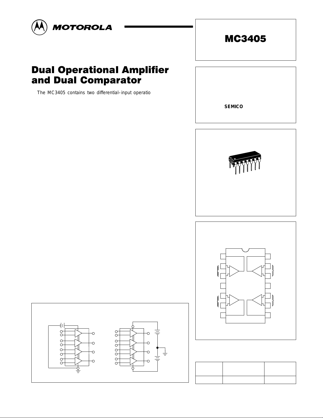
DUAL OPERATIONAL
AMPLIFIER / DUAL
VOLTAGE COMPARATOR
SEMICONDUCTOR
TECHNICAL DATA
14
1
Single Supply
3.0 V to 36 V
P SUFFIX
PLASTIC PACKAGE
CASE 646
PIN CONNECTIONS
1
Out 1
Inputs 1
V
CC
Inputs 2
Split Supplies
V
CC
1
2
V
CC
1
2
1.5 V to 18 V
Out 2
Comp
1
2
(Top View)
Amp 1
Amp 2
2
+
14
–
3
4
Comp
5
+
23
–
6
7
Op
Op
14
Out 4
13
–
+
+
–
12
11
10
9
8
Inputs 4
VEE/Gnd
Inputs 3
Out 3
3
4
VEE, Gnd
MOTOROLA ANALOG IC DEVICE DATA
3
4
V
EE
1.5 V to 18 V
MC3405P TA = 0° to +70°C Plastic DIP
Motorola, Inc. 1996 Rev 1
ORDERING INFORMATION
Operating
Device
Temperature Range
Package
1
Page 2
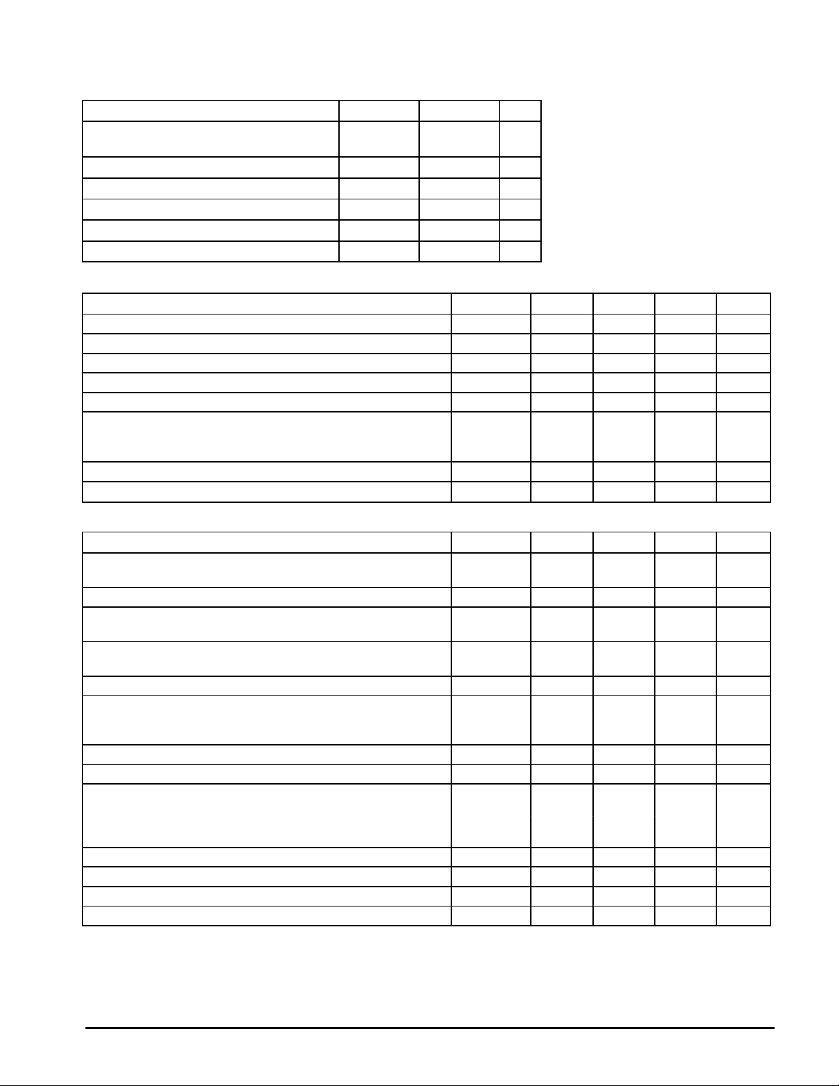
OPERATIONAL AMPLIFIER SECTION
MAXIMUM RATINGS
Rating Symbol Value Unit
Power Supply Voltage – Single Supply
Power Supply Voltage – Split Supplies
Input Differential Voltage Range V
Input Common Mode Voltage Range V
Operating Ambient Temperature Range T
Storage Temperature Range
Operating Junction Temperature Range T
VCC, V
V
IDR
ICR
Tstg
CC
EE
A
J
MC3405
0 to +70 °C
–55 to +125 °C
36
±18
±36 Vdc
±18 Vdc
150 °C
Vdc
ELECTRICAL CHARACTERISTICS (V
Characteristic
Input Offset Voltage V
Input Offset Current I
Input Bias Current I
Large–Signal, Open Loop Voltage Gain (RL = 2.0 kΩ) A
Power Supply Rejection PSR – – 150 µV/V
Output Voltage Range (Note 1) V
(RL = 10 kΩ, VCC = 5.0 V) 3.3 3.5 –
(RL = 10 kΩ, 5.0 V ≤ VCC ≤ 30 V) VCC–2.0 VCC –1.7 –
Power Supply Current (Notes 2 and 3) I
Channel Separation, f = 1.0 kHz to 20 kHz (Input Referenced) – – –120 – dB
ELECTRICAL CHARACTERISTICS (V
Characteristic
Input Offset Voltage V
(TA = T
Average Temperature Coefficient of Input Offset Voltage ∆VIO/∆T – 15 – µV/°C
Input Offset Current I
(TA = T
Input Bias Current I
(TA = T
Input Common Mode Voltage Range V
Large Signal, Open Loop Voltage Gain A
(VO = ±10 V, RL = 2.0 kΩ) 20 200 –
(TA = T
Common Mode Rejection CMR 70 90 – dB
Power Supply Rejection Ratio PSRR – 30 150 µV/V
Output Voltage V
(RL = 10 kΩ) ±12 ±13.5 –
(RL = 2.0 kΩ) ±10 ±13 –
(RL = 2.0 kΩ, TA = T
Output Short Circuit Current I
Power Supply Current (Notes 2 and 3) ICC, I
Phase Margin φm – 60 – Degrees
Small–Signal Bandwidth (AV = 1, RL = 10 kΩ, VO = 50 mV) BW – 1.0 – MHz
NOTES: 1. Output will swing to ground.
+ T
low
low
low
low
2.Not to exceed maximum package power dissipation.
3.For operational amplifier and comparator.
4.T
low
) (Note 4) – – 12
high
to T
to T
to T
= 0°C, T
) (Note 4) – – 200
high
) (Note 4) – – –800
high
) (Note 4) 15 100 –
high
high
to T
low
= +70°C
) (Note 4) ±10 – –
high
= 5.0 V, VEE = Gnd, TA = 25°C, unless otherwise noted.)
CC
Symbol Min Typ Max Unit
IO
IO
IB
VOL
OR
CC
= +15 V, VEE = –15 V, TA = 25°C, unless otherwise noted.)
CC
Symbol Min Typ Max Unit
IO
IO
IB
ICR
VOL
O
SC
EE
– 2.0 10 mV
– 30 50 nA
– –200 –500 nA
20 200 – V/mV
– 2.5 7.0 mA
– 2.0 10 mV
– – 50 nA
– –200 –500 nA
+13 –V
±10 ±20 ±45 mA
– 2.8 7.0 mA
EE
V
pp
– – Vdc
V
/mV
Vdc
2
MOTOROLA ANALOG IC DEVICE DATA
Page 3
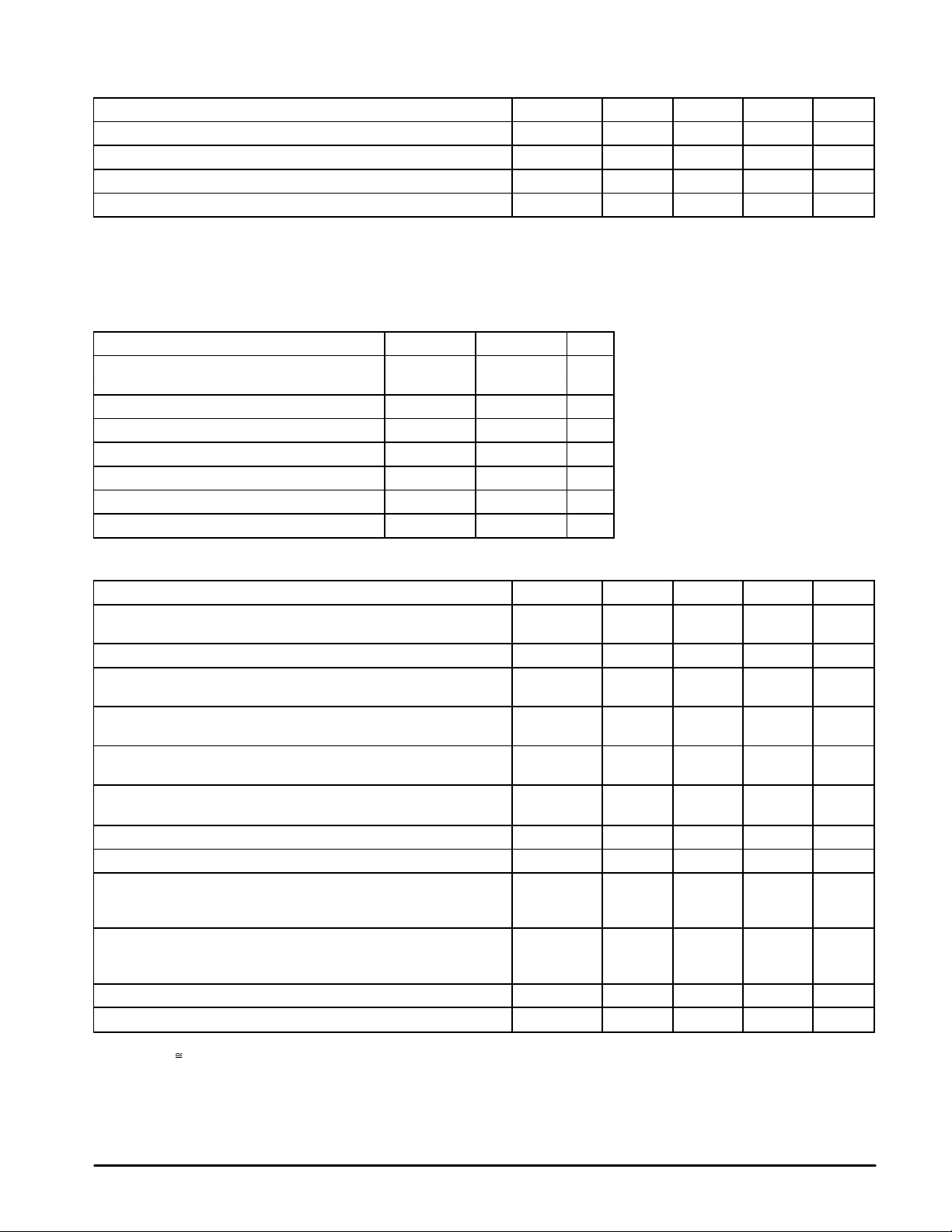
MC3405
ELECTRICAL CHARACTERISTICS (V
Characteristic
Power Bandwidth (AV = 1, RL = 2.0 kΩ, VO = 20 Vpp, THD = 5%) BWp – 9.0 – kHz
Rise Time/Fall Time t
Overshoot (AV = 1, RL = 10 kΩ, VO = 50 mV) os – 20 – %
Slew Rate SR – 0.6 – V/µs
= +15 V, VEE = –15 V, TA = 25°C, unless otherwise noted.)
CC
Symbol Min Typ Max Unit
TLH
, t
THL
– 0.35 – µs
COMPARATOR SECTION
MAXIMUM RATINGS
Rating Symbol Value Unit
Power Supply Voltage – Single Supply V
Power Supply Voltage – Split Supplies VCC, V
Input Differential Voltage Range V
Input Common Mode Voltage Range V
Sink Current I
Operating Ambient Temperature Range T
Storage Temperature Range
Operating Junction Temperature Range T
CC
IDR
ICR
Sink
A
Tstg
EE
J
36 Vdc
±18
±36 Vdc
–0.3 to +36 Vdc
20 mA
0 to +70 °C
–55 to +125 °C
150 °C
ELECTRICAL CHARACTERISTICS (V
Characteristic
Input Offset Voltage V
(TA = T
Average Temperature Coefficient of Input Offset Voltage ∆VIO/∆T – 15 – µV/°C
Input Offset Current I
(TA = T
Input Bias Current I
(TA = T
Input Common Mode Voltage Range V
(TA = T
Input Differential Voltage
(All Vin ≥ 0 Vdc)
Large–Signal, Open Loop Voltage Gain (RL = 15 kΩ) A
Output Sink Current (–Vin ≥ 1.0 Vdc, +Vin= 0, VO ≤ 1.5 V) I
Low Level Output Voltage
(+Vin= 0 V, –Vin= 1.0 V, I
(TA = T
Output Leakage Current I
(+Vin ≥ 1.0 Vdc, –Vin= 0, VO = 5.0 Vdc) – 0.1 1.0
(TA = T
Large–Signal Response – – 300 – ns
Response Time (Note 3) (VRL = 5.0 Vdc, RL = 5.1 kΩ) – – 1.3 – µs
NOTES: 1. T
to T
low
to T
low
to T
low
to T
low
to T
low
to T
low
= 0°C, T
low
2.VO ^ 1.4 V, RS = 0 Ω with VCC from 5.0 Vdc to 30 Vdc, and over the input common mode range 0 to VCC –1.7 V.
3.The response time specified is for a 100 mV input step with 5.0 mV overdrive. For larger signals 300 ns is typical.
) (Notes 1 and 2) – – 12
high
) (Note 1) – – 200
high
) (Note 1) – – –800
high
) (Note 1) 0 VCC –1.7 VCC –2.0
high
= 4.0 mA)
Sink
) (Note 1)
high
) (Note 1) – 0.1 1.0
high
= +70°C
high
= 5.0 V, VEE = Gnd, TA = 25°C, unless otherwise noted.)
CC
Symbol Min Typ Max Unit
IO
IO
IB
ICR
V
ID
VOL
Sink
V
OL
OL
6.0 16 – mA
– 2.0 10 mV
– 50 100 nA
– –125 –500 nA
0 VCC –1.5 VCC –1.7 Vpp
– – 36 V
– 200 – V
–
–
350
–
500
700
/mV
µA
µA
MOTOROLA ANALOG IC DEVICE DATA
3
Page 4
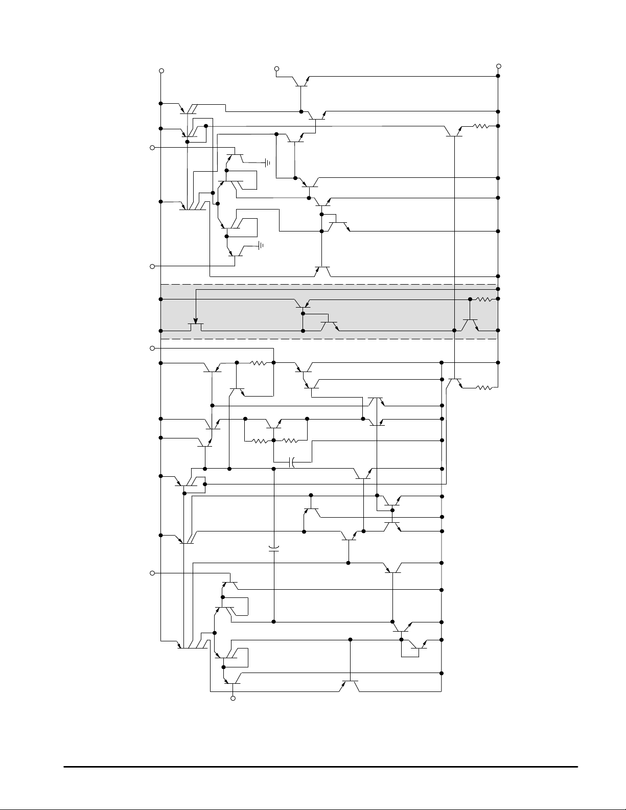
MC3405
CC
V
(–)
2, 6 3, 5
(+)
Output
8,14
Q41
Q1
11
/Gnd
EE
V
700
Comparator Side
2.4 k
Comparators
to All Op Amps and
Bias Circuitry Common
Output
25
1,7
Q34
Q35
Q40
Q36
Q37
Q38
Q39
Q43
Q42
Q28
Q12
Q11
4
Q32Q31
Q33
Q29
Q26 Q30
Q27
Q16
Q15
(1/2 of Circuit Shown)
Q17Q18
Representative Schematic Diagram
Q19
Q20
10,12
(+)
Q21
Q22Q24
Q23
Q25
(–)
9, 13
Q14
Q13
34.4 k
30
31.2 k
pF
Q7
Q6
5.0 pF
Q2
Q10
Q9
Q8
Q27
Q5
Q4
Q3
2.0 k
Operational Amplifier Side
4
MOTOROLA ANALOG IC DEVICE DATA
Page 5

OPERATIONAL AMPLIFIER SECTION
Figure 1. Sine Wave Response Figure 2. Open Loop Frequency Response
AV = 100
50 mV/DIV 0.5 V/DIV
*Note Class A B output stage produces distortion less sinewave.
50 µs/DIV
Figure 3. Power Bandwidth Figure 4. Output Swing versus Supply Voltage
30
pp
25
20
15
+15 V
–
+
–15 V
10 k
V
O
MC3405
, LARGE SIGNAL
VOL
A
120
100
80
60
40
20
0
OPEN LOOP VOLTAGE GAIN (dB)
–20
1.0 10 100 1.0 k 10 k 100 k 1.0 M
f, FREQUENCY (Hz)
30
pp
20
VCC = 15 V
VEE = –15 V
°
C
TA = 25
TA = 25°C
10
5.0
, OUTPUT VOLTAGE (V )
O
TA = 25°C
V
0
–5.0
1.0 k 10 k 100 k 1.0 M
f, FREQUENCY (Hz)
Figure 5. Input Bias Current
versus T emperature
300
200
100
, INPUT BIAS CURRENT (nA)I
IB
–75 –55 –35 –15 5.0 25 45 65 85 105 125
T, TEMPERATURE (°C)
VCC = 15 V
VEE = –15 V
TA = 25
10
, OUTPUT VOLTAGE RANGE (V )
O
V
0
0 2.0 4.0 6.0 8.0 10 12 14 16 18 20
VCC AND |VEE|, POWER SUPPLY VOLTAGES (V)
Figure 6. Input Bias Current
versus Supply V oltage
°
C
170
160
, INPUT BIAS CURRENT (nA)I
IB
150
0 2.0 4.0 6.0 8.0 10 12 14 16 18 20
VCC AND |VEE|, POWER SUPPLY VOLTAGES (V)
MOTOROLA ANALOG IC DEVICE DATA
5
Page 6

MC3405
COMPARATOR SECTION
Figure 7. Normalized Input Offset Voltage Figure 8. Input Bias Current
1.40
200
1.20
°
1.00
0.80
NORMALIZED TO 25 C
INPUT OFFSET VOLTAGE
0.60
0.40
–60 –40 –20 0 20 40 60 80 100 120 140
VCC = +15 V
VEE = Gnd
Slope Can Be Either Polarity.
TA, AMBIENT TEMPERATURE (°C)
Figure 9. Normalized Input Offset Current
2.20
1.80
°
1.40
1.00
NORMALIZED TO 25 C
INPUT OFFSET VOLTAGE
0.60
Slope Can Be Either Polarity.
0.20
–60 –40 –20 0 20 40 60 80 100 120 140
TA, AMBIENT TEMPERATURE (°C)
VCC = +15 V
VEE = Gnd
160
120
80
, INPUT BIAS CURRENT (nA)I
IB
40
2.0 6.0 10 14 18 22 26 30
TA = –55°C
°
TA = +25
VCC, POSITIVE SUPPLY VOLTAGE (V)
C
TA = +125°C
VEE = Gnd
Figure 10. Output Sink Current versus
Output Voltage
7.0
6.0
5.0
4.0
3.0
2.0
1.0
Sink
I , OUTPUT SINK CURRENT (mA)
0
0 200 400 600 800 1000
TA = –55°C
TA = +125°C
VOL, OUTPUT VOLTAGE (mV)
TA = +25°C
VCC = +15 V
VEE = Gnd
Figure 11. Pulse Width Modulator Schematic and Waveforms
1.0 M
1
12
13
EE
EE
R1
4RfCR2
5.0 k
300 k
R1
+
Amp 1
–
V
V
CC
5.0 k
5.0 k
V
EE
10 k
C
10
+
Amp 2
–
9
C
VTH = VS(1 + R2/R1) + V
VTL = VS(1 – R2/R1) + V
Oscillator Frequency f =
2
+
Comp 1
3
–
8
v
t
150 k
R2
R
f
1
2
1
2
V
CC
4
+
Comp 2
6
–
5
11
V
EE
14
V
SW
VS = VCC – V
EE
5.0 k
7
V
out
V
SW
V
CC
V
EE
V
TH
V
TL
V
out
V
CC
V
EE
Pulse Width = when: VTL < VC < V
Duty Cycle in % = (100)
(a) Oscillator Square Wave Output
(b) Triangle Wave and Control Voltage
v
t
(c) Output Pulses
f
VTH–V
Vc – V
VTH–V
Vc – V
TL
TL
TL
TL
1
V
Time
C
Time
Time
TH
6
MOTOROLA ANALOG IC DEVICE DATA
Page 7

V
CC
∆
V
Adjust
10 k
13
12
Amp 1
10 k
V
CC
10 k
VC Adjust
V
EE
C3
V
C1
in
C2
R1
High Pass Filter
High Pass Filter
Given: Ao, Q,
ω
f
= 2
o
o
π
Choose: C = C1 = C2, a convenient value
C3 =
R1 =
Q
ω
C
o
C
A
o
A
o
Q
ω
C(2Ao + 1) R
o
Calculate: R2 = (2Ao + 1)
–
+
R2
10 k
13
12
MC3405
Figure 12. Window Comparator
14
10 k
10 k
9
10
–
Amp 2
+
8
Figure 13. Squelch Circuit for AM or FM
–
14
Amp 1
+
C4
R3C4 > 5 T
Where : Tin is the period of V
Q = Quality Factor
Ao = High Frequency Gain
ωo = Break Frequency
5
–
Comp 2
6
+
11
V
3
–
Comp 1
2
+
V
in
R3
V
CC
in
V
CC
4
7
EE
1
3
2
Squelch
Threshold Adj
in
3.0 k
–
Comp 1
+
100 k
V
O
13
∆
V
∆
V
V
in
v
O
–13
V
C
V
CC
2.7 k
1
2.7 k
10
+
Amp 2
9
–
R
i
V
Ai
Switched Audio Stage
8
R
f
V
AO
Gain of Audio Stage
R
f
ACI =
i
V
CC
R1
1.0 k
V
i
1.0 k
R2
3
2
5
6
–
Comp 1
+
–
Comp 2
+
1
7
Hi/Low
R3
Limit Detector
MOTOROLA ANALOG IC DEVICE DATA
Figure 14. High/Low Limit Alarm
V
10 k
R4
10 k
R5
2.0 k
2.0 k
V
C
CC
V
CC
C
12
13
10
0.01
9
µ
F
10 k
R6
+
Amp 1
–
Rf 33 k
+
Amp 2
–
14
V
C
V
CC
Oscillator
8
V
O
0
VIL = V
VIH = V
VILV
CC
R1 + R2 + R3
R2 + R3
CC
R1 + R2 + R3
V
IH
i
R3
Oscillator
If R4 = R5 = R6
f = 0.72/RfC
As shown, f = 2.2 kHz
VO will oscillate if VIH < Vi, or VIL > V
VO will be low if VIL < Vi < V
i
IH
7
Page 8

MC3405
Figure 15. Zero Crossing Detector with T emperature Sensor
V
10 k
V
CC
V
in
R1
V
EE
1N914
R2
1N914
10 k
2
+
Comp 1
3
–
+
V
D
–
6
+
+
V
D
Comp 2
5
–
–
Zero Crossing Detector
1
7
Temp
Adjust
10 k
13
Q1
V
CC
R6
R8
V
CC
R7
R3
R4
T emperature Sensor
R5
10
v
9
t
1.0 M
+
Amp 2
–
10 k
8
12
13
10 k
CC
+
Amp 1
–
V
EE
V
+V
–V
O
S
0
S
v
o
V
CC
V
EE
Vt = (VBE of Q1)
2V
13 >
±
VS = ±V
BE
R5
R1 + R2
D
R2
14
R1 and R2 control the switching
voltage of the zero crossing detector
TA < T
Set
R4 + R5
R5
Time
Figure 16. LSTTL to CMOS Interface with Hysteresis Figure 17. NOR Gate
+ 5.0 V
LSTTL Level Shift
*The same configuration may be used with an op amp if
the 3.0 k resistor is removed.
2.4 k
27 k
–
Comp *
+
50 k
VIL = 1.17 V
VIH = 1.80 V
3.0 k *
+ 15 V
CMOS
A
B
C
D
*The same configuration may be used with an
op amp if the 3.0 k resistor is removed.
V
CC
10 k
+
Comp *
–
10 k 10 k
G = A + B + C + D
3.0 k*
G
8
MOTOROLA ANALOG IC DEVICE DATA
Page 9

MC3405
OUTLINE DIMENSIONS
P SUFFIX
PLASTIC PACKAGE
CASE 646–06
14 8
B
17
A
F
N
SEATING
HG D
PLANE
C
K
L
J
M
ISSUE L
NOTES:
1. LEADS WITHIN 0.13 (0.005) RADIUS OF TRUE
POSITION AT SEATING PLANE AT MAXIMUM
MATERIAL CONDITION.
2. DIMENSION L TO CENTER OF LEADS WHEN
FORMED PARALLEL.
3. DIMENSION B DOES NOT INCLUDE MOLD
FLASH.
4. ROUNDED CORNERS OPTIONAL.
DIM MIN MAX MIN MAX
A 0.715 0.770 18.16 19.56
B 0.240 0.260 6.10 6.60
C 0.145 0.185 3.69 4.69
D 0.015 0.021 0.38 0.53
F 0.040 0.070 1.02 1.78
G 0.100 BSC 2.54 BSC
H 0.052 0.095 1.32 2.41
J 0.008 0.015 0.20 0.38
K 0.115 0.135 2.92 3.43
L 0.300 BSC 7.62 BSC
M 0 10 0 10
____
N 0.015 0.039 0.39 1.01
MILLIMETERSINCHES
MOTOROLA ANALOG IC DEVICE DATA
9
Page 10

MC3405
NOTES
10
MOTOROLA ANALOG IC DEVICE DATA
Page 11

MC3405
NOTES
MOTOROLA ANALOG IC DEVICE DATA
11
Page 12

MC3405
Motorola reserves the right to make changes without further notice to any products herein. Motorola makes no warranty , representation or guarantee regarding
the suitability of its products for any particular purpose, nor does Motorola assume any liability arising out of the application or use of any product or circuit, and
specifically disclaims any and all liability, including without limitation consequential or incidental damages. “T ypical” parameters which may be provided in Motorola
data sheets and/or specifications can and do vary in different applications and actual performance may vary over time. All operating parameters, including “Typicals”
must be validated for each customer application by customer’s technical experts. Motorola does not convey any license under its patent rights nor the rights of
others. Motorola products are not designed, intended, or authorized for use as components in systems intended for surgical implant into the body, or other
applications intended to support or sustain life, or for any other application in which the failure of the Motorola product could create a situation where personal injury
or death may occur. Should Buyer purchase or use Motorola products for any such unintended or unauthorized application, Buyer shall indemnify and hold Motorola
and its officers, employees, subsidiaries, affiliates, and distributors harmless against all claims, costs, damages, and expenses, and reasonable attorney fees
arising out of, directly or indirectly, any claim of personal injury or death associated with such unintended or unauthorized use, even if such claim alleges that
Motorola was negligent regarding the design or manufacture of the part. Motorola and are registered trademarks of Motorola, Inc. Motorola, Inc. is an Equal
Opportunity/Affirmative Action Employer.
How to reach us:
USA/EUROPE/Locations Not Listed: Motorola Literature Distribution; JAPAN: Nippon Motorola Ltd.; Ta tsumi–SPD–JLDC, 6F Seibu–Butsuryu–Center,
P.O. Box 20912; Phoenix, Arizona 85036. 1–800–441–2447 or 602–303–5454 3–14–2 Tatsumi Koto–Ku, Tokyo 135, Japan. 03–81–3521–8315
MFAX: RMF AX0@email.sps.mot.com – TOUCHT ONE 602–244–6609 ASIA/PACIFIC: Motorola Semiconductors H.K. Ltd.; 8B Tai Ping Industrial Park,
INTERNET: http://Design–NET.com 51 Ting Kok Road, Tai Po, N.T., Hong Kong. 852–26629298
12
◊
MOTOROLA ANALOG IC DEVICE DATA
MC3405/D
*MC3405/D*
 Loading...