

Page 1
SEMICONDUCTOR
TECHNICAL DATA
HEX EIA–485 TRANSCEIVER
with THREE–STATE OUTPUTS
Order this document by MC34058/D
FTA SUFFIX
PLASTIC PACKAGE
CASE 932
(Thin QFP)
148
Device
Operating
Temperature Range
Package
ORDERING INFORMATION
MC34058FTA
MC34059FTA
TA = 0° to +70°C TQFP–48
1
MOTOROLA ANALOG IC DEVICE DATA
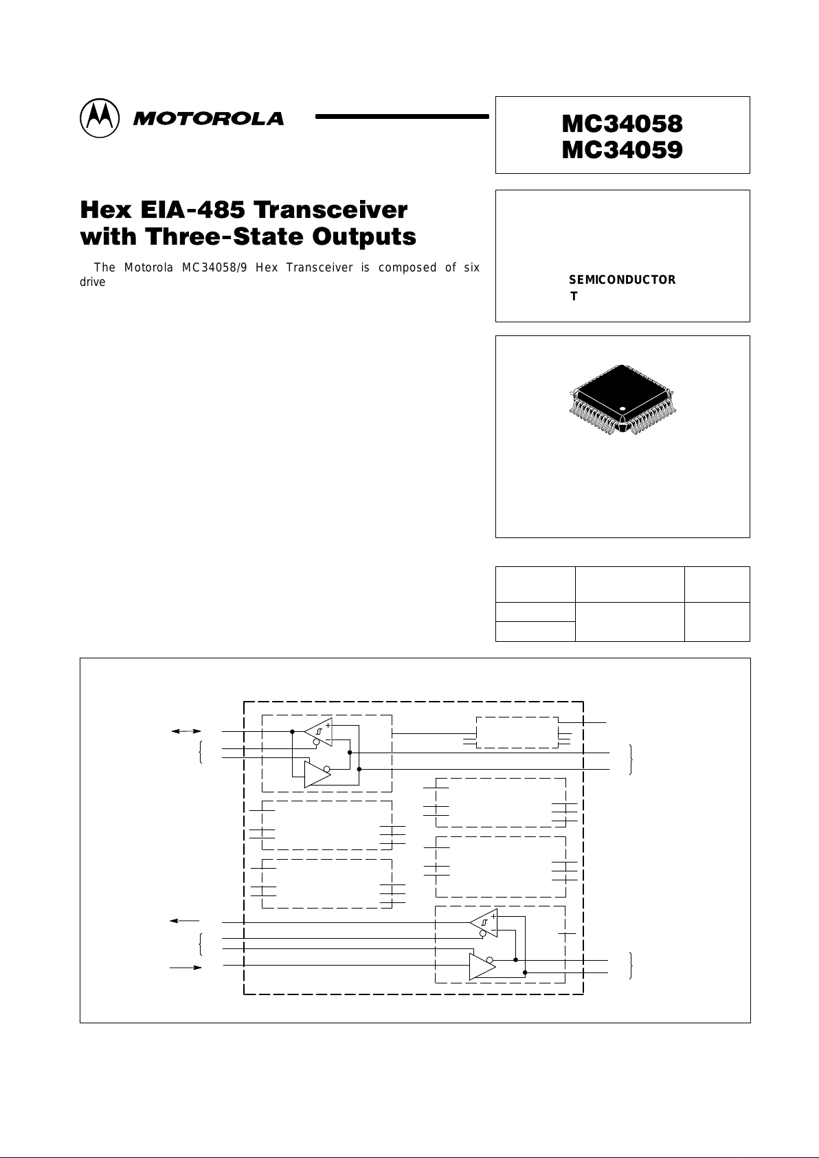
The Motorola MC34058/9 Hex Transceiver is composed of six
driver/receiver combinations designed to comply with the EIA–485 standard.
Features include three–state outputs, thermal shutdown for each driver, and
current limiting in both directions. This device also complies with EIA–422
and CCITT Recommendations V.11 and X.27.
The devices are optimized for balanced multipoint bus transmission at
rates to 20 MBPS (MC34059). The driver outputs/receiver inputs feature a
wide common mode voltage range, allowing for their use in noisy
environments. The current limit and thermal shutdown features protect the
devices from line fault conditions.
The MC34058/9 is available in a space saving 7.0 mm 48 lead surface
mount quad package designed for optimal heat dissipation.
• Meets EIA–485 Standard for Party Line Operation
• Meets EIA–422A and CCITT Recommendations V.11 and X.27
• Operating Ambient Temperature: 0°C to +70°C
• Common Mode Driver Output/Receiver Input Range: –7.0 to +12 V
• Positive and Negative Current Limiting
• Transmission Rates to 14 MBPS (MC34058) and 20 MBPS (MC34059)
• Driver Thermal Shutdown at 150°C Junction Temperature
• Thermal Shutdown Active Low Output
• Single +5.0 V Supply, ±10%
• Low Supply Current
• Compact 7.0 mm 48 Lead TQFP Plastic Package
Representative Block Diagram
This device contains 1,399 active transistors.
TTL/CMOS Data DR
Direction
Control
RE
DE
Thermal
Shutdown
OB
OA
To Cable
Thermal
Shutdown
(Same as #1)
(Same as #1)
(Same as #1)
(Same as #1)
#3
#5
#4
#2
#1
TSD
#6
TSD
OB
OA
To Cable
TTL/CMOS Data RO
Direction
Control
RE
DE
TTL/CMOS Data DI
D
D
Motorola, Inc. 1996 Rev 1
Page 2
MC34058 MC34059
2
MOTOROLA ANALOG IC DEVICE DATA
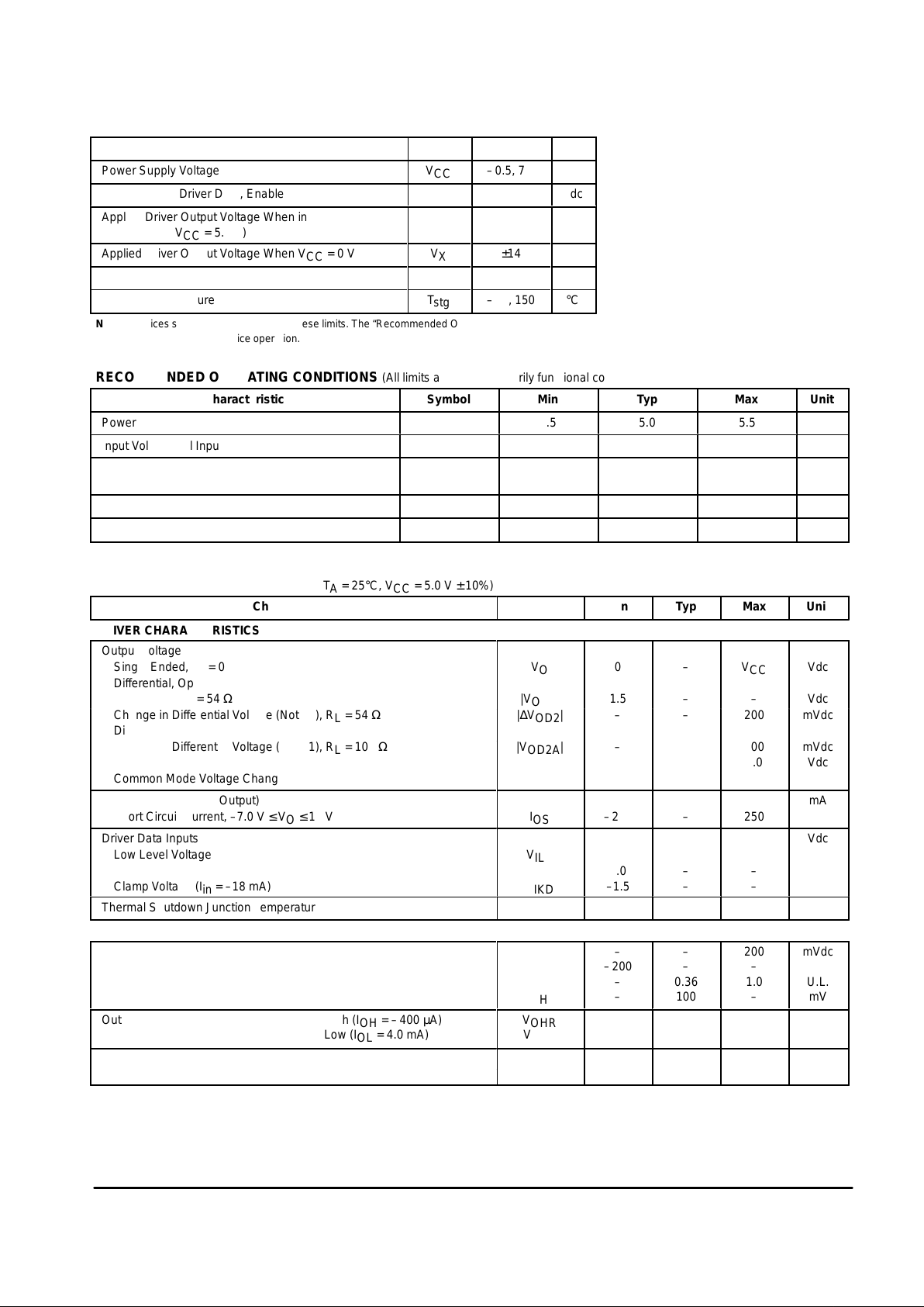
MAXIMUM RATINGS
Rating Symbol Value Unit
Power Supply Voltage
V
CC
–0.5, 7.0
Vdc
Input Voltage (Driver Data, Enables)
V
in
7.0
Vdc
Applied Driver Output Voltage When in Three–State
V
Z
–10, 14
Vdc
Condition (VCC = 5.0 V)
Applied Driver Output Voltage When VCC = 0 V
V
X
±14
Vdc
Output Current
I
O
Self Limiting
–
Storage Temperature
T
stg
–65, 150
°C
NOTE: Devices should not be operated at these limits. The “Recommended Operating Conditions”
provides for actual device operation.
RECOMMENDED OPERATING CONDITIONS (All limits are not necessarily functional concurrently.)
Characteristic
Symbol Min Typ Max Unit
Power Supply Voltage
V
CC
4.5
5.0
5.5
Vdc
Input Voltage (All Inputs Except Receiver Inputs)
V
in
0
–
V
CC
Vdc
Driver Output Voltage in Three–State Condition,
V
CM
–7.0
–
12
Vdc
Receiver Inputs, or When VCC = 0 V
БББББББББББББ
Driver Output Current (Normal Data Transmission)
ÁÁÁ
I
O
ÁÁÁ
–60
ÁÁÁÁ–ÁÁÁ60Á
mA
БББББББББББББ
Á
Operating Ambient Temperature
ÁÁÁ
Á
T
A
ÁÁÁ
Á
0
ÁÁÁÁ
Á
–
ÁÁÁ
Á
70
Á
Á
°C
ELECTRICAL CHARACTERISTICS (T
A
= 25°C, VCC = 5.0 V ± 10%)
Characteristic
Symbol Min Typ Max Unit
DRIVER CHARACTERISTICS
Output Voltage
ÁÁÁ
Single Ended, IO = 0 V
O
0 – V
CC
Vdc
Differential, Open Circuit (IO = 0) |V
OD1
| 1.5 – – Vdc
Differential, RL = 54 Ω |V
OD2
| 1.5 – – Vdc
Change in Differential V oltage (Note 1), RL = 54 Ω |∆V
OD2
| – – 200 mVdc
Differential, RL = 100 Ω |∆V
OD2A
| 2.0 – – Vdc
Change in Differential V oltage (Note 1), RL = 100 Ω |V
OD2A
| – – 200 mVdc
Common Mode Voltage, RL = 54 Ω V
OCM
– – 3.0 Vdc
Common Mode Voltage Change, RL = 54 Ω |∆V
OCM
| – – 200 mVdc
Output Current (Each Output)
ÁÁÁ
mA
Short Circuit Current, –7.0 V ≤ VO ≤ 12 V I
OS
–250 – 250
Driver Data Inputs
ÁÁÁ
Vdc
Low Level Voltage V
ILD
– – 0.8
High Level Voltage V
IHD
2.0 – –
Clamp Voltage (Iin = –18 mA) V
IKD
–1.5 – –
Thermal Shutdown Junction Temperature
T
JTS
–
150
–
ÁÁÁ
°C
RECEIVER CHARACTERISTICS
БББББББББББББББББ
Á
БББББББББББББББББ
Á
Input Threshold RO = High
RO = Low
Input Loading (Driver Disabled)
Hysteresis
ÁÁÁ
Á
ÁÁÁ
Á
V
th
V
H
ÁÁ
Á
ÁÁ
Á
–
–200
–
–
ÁÁ
Á
ÁÁ
Á
–
–
0.36
100
ÁÁ
Á
ÁÁ
Á
200
–
1.0
–
ÁÁÁ
ÁÁ
Á
ÁÁ
Á
mVdc
U.L.
mV
Output Voltage High (IOH = –400 µA)
Low (IOL = 4.0 mA)
V
OHR
V
OLR
2.4
–
–
–
–
0.4
ÁÁÁ
Vdc
Output Short Circuit Current
I
OSR
–
45
85
ÁÁÁ
mA
Output Leakage Current When in Three–State Mode I
OLKR
– – 20 µA
NOTE: 1. Input switched from low to high.
Page 3
MC34058 MC34059
3
MOTOROLA ANALOG IC DEVICE DATA
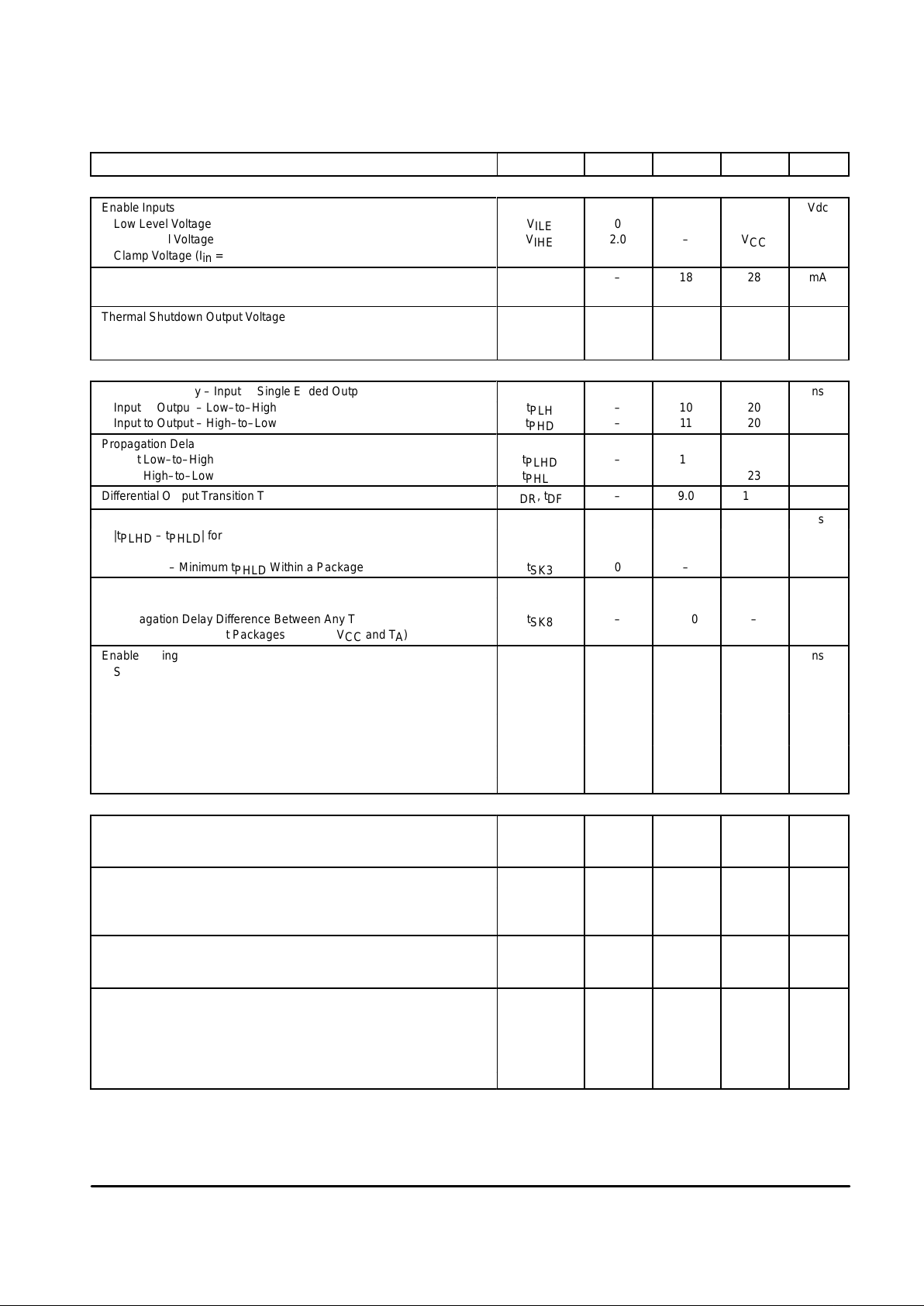
ELECTRICAL CHARACTERISTICS (continued) (T
A
= 25°C, VCC = 5.0 V ± 10%)
Characteristic UnitMaxTypMinSymbol
MISCELLANEOUS
Enable Inputs
ÁÁÁ
Vdc
Low Level Voltage V
ILE
0 – 0.8
High Level Voltage V
IHE
2.0 – V
CC
Clamp Voltage (Iin = –18 mA) V
IKE
–1.5 – –
Power Supply Current (Total Package, All Outputs Open, Enabled
or Disabled)
I
CC
–
18
28
ÁÁÁ
mA
БББББББББББББББББ
Á
БББББББББББББББББ
Á
Thermal Shutdown Output Voltage
High
Low
ÁÁÁ
Á
ÁÁÁ
Á
V
OHT
V
OLT
ÁÁ
Á
ÁÁ
Á
2.4
0
ÁÁ
Á
ÁÁ
Á
–
–
ÁÁ
Á
ÁÁ
Á
–
0.8
ÁÁÁ
ÁÁ
Á
ÁÁ
Á
Vdc
TIMING CHARACTERISTICS – DRIVER
Propagation Delay – Input to Single Ended Output
ns
Input to Output – Low–to–High t
PLH
– 10 20
Input to Output – High–to–Low t
PHD
– 11 20
Propagation Delay – Input to Differential Output
ÁÁÁ
ns
Input Low–to–High t
PLHD
– 15 23
Input High–to–Low t
PHLD
– 15 23
Differential Output Transition T ime
tDR, t
DF
–
9.0
10.7
ÁÁÁ
ns
Skew Timing MC34058 ns
|t
PLHD
– t
PHLD
| for Each Driver t
SK1
0 0.1 –
Maximum – Minimum t
PLHD
Within a Package t
SK2
0 – 8.0
Maximum – Minimum t
PHLD
Within a Package t
SK3
0 – 6.0
Skew Timing MC34059 ns
|t
PLHD
– t
PHLD
| for Each Driver t
SK7
0 0.1 –
Propagation Delay Difference Between Any Two Drivers (Same
Package or Different Packages at Same VCC and TA)
t
SK8
– <4.0 –
Enable Timing ns
Single Ended Outputs
Enable to Active High Output t
PZH
– 15 40
Enable to Active Low Output t
PZL
– 25 40
Active High to Disable t
PHZ
– 12 25
Active Low to Disable t
PLZ
– 10 25
Differential Outputs
Enable to Active Output t
PZD
– – 40
Enable to Three–State Output t
PDZ
– – 25
TIMING CHARACTERISTICS – RECEIVER
Propagation Delay ns
Input to Output – Low–to–High t
PLHR
– 16 23
Input to Output – High–to–Low t
PHLR
– 16 23
Skew Timing ns
|t
PLHR
– t
PHLR
| for Each Receiver t
SK4
0 1.0 –
Maximum – Minimum t
PLHR
Within a Package t
SK5
0 – 3.0
Maximum – Minimum t
PHLR
Within a Package t
SK6
0 – 3.0
Skew Timing t
SK9
– <5.0 – ns
Propagation Delay Difference Between Any Two Receivers in Different
Packages at Same VCC and TA (MC34059 Only)
Enable Timing ns
Single Ended Outputs
Enable to Active High Output t
PZHR
– 15 22
Enable to Active Low Output t
PZLR
– 25 30
Active High to Disable t
PHZR
– 12 25
Active Low to Disable t
PLZR
– 10 25
Page 4
MC34058 MC34059
4
MOTOROLA ANALOG IC DEVICE DATA
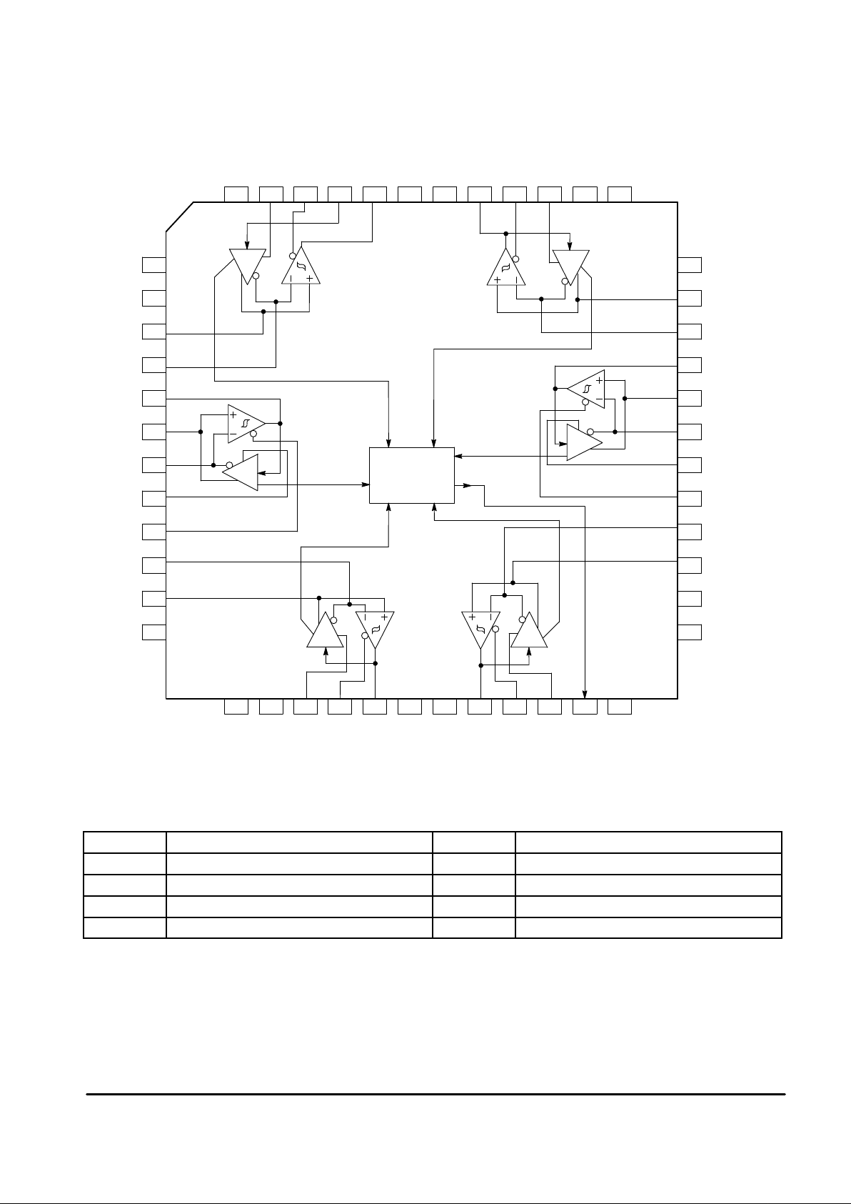
Block Diagram and Pinout
MC34058/9
Thermal
Shutdown
Indicator
Gnd
1
Gnd Gnd Gnd
GndDE5RE5DR5V
CC
V
CC
RO6DI6RE6DE6
DE2 RE2 DR2 VCCVCCDR3 RE3 DE3 TSD
Gnd
OA5
OB5
DR4
OA4
OB4
DE4
RE4
OB3
OA3
Gnd
Gnd
#4
#5
#6
#3
#2
#1
Gnd
Gnd
OA6
OB6
DR1
OA1
OB1
DE1
RE1
OB2
OA2
Gnd
2
3
4
5
6
7
8
9
10
11
12
36
35
34
33
32
31
30
29
28
27
26
18 19 20 21 22 23 24
25
1716151413
43 42 41 40 39 38 374445464748
Gnd
D
D
D
D
D
D
PINOUT SUMMARY
OA NonInverting Output/Input DE Driver Enable, Active High (TTL)
OB Inverting Output/Input RE Receiver Enable, Active Low (TTL)
DR Driver Input/Receiver Output (TTL) TSD Thermal Shutdown Indicator
DI6 #6 Driver Input (TTL) V
CC
Connect 4 Pins to 5.0 V , ±10%
RO6 #6 Receiver Output (TTL) Gnd Connect 12 Pins to Circuit Ground
Page 5

MC34058 MC34059
5
MOTOROLA ANALOG IC DEVICE DATA
V
CC
27
15 pF
2.3 V
Output
S.G.
3.0 V
3.0 V
3.0 V
3.0 V
3.0 V
1.5 V
1.5 V
0 V
V
OL
V
OH
Figure 1. VOD and VOS Test Circuit
Figure 2. VOD and VCM Test Circuit
Figure 3. VOD AC Test Conditions
Figure 4. VOH and VOL AC Test Conditions
V
CC
R
L/2
R
L/2
V
OS
V
OD2, A
V
in
(0.8 or 2.0 V)
375
375
58
V
CM
(+12 to
±
7.0 V)
50 pF
S.G.
V
OD
V
in
t
PLHD
t
PHLD
50%
50%
3.0 V
1.5 V
1.5 V
OAX
0 V
V
OD
t
dr
t
dr
V
CC
V
OD2, A
V
in
(0.8 or 2.0 V)
54
V
CC
V
in
OAX
OBX
t
PLH
t
PLH
t
PHL
t
PHL
Page 6

MC34058 MC34059
6
MOTOROLA ANALOG IC DEVICE DATA
Figure 5. VOH versus I
OH
–10
0.4
0
1.1
–100
4.0
–80
4.6
INPUT CURRENT (mA)
INPUT VOLTAGE (V)
IOL (mA)
IOD (mA)
V
ODH
V
OH
(V)
IOH (mA)
Figure 6. VOL versus I
OL
Figure 7. VOD versus I
OL
Figure 8. Input Characteristics of
OAX and OAB
V
OL
(V)
V
OD
(V)
– 60 – 40 – 20 0 20 10 20 30 40 50 60 70 80
– 5.0 0 5.0 10 15– 50 0 50 100
4.4
4.2
4.0
3.8
0.9
1.0
0.8
0.6
0.7
0.5
0.3
0.1
– 0.1
– 0.3
– 0.4
– 0.2
0
0.2
2.0
0
– 2.0
– 4.0
3.6
V
ODL
OAX_lin(mA)
OBX_lin(mA)
Description
The MC34058/9 is a differential line driver designed to
comply with EIA–485 Standard for use in balanced digital
multipoint systems containing multiple drivers. The drivers
also comply with EIA–422–A and CCITT Recommendations
V.11 and X.27. Positive and negative current limiting of the
drivers meet the EIA–485 requirement for protection from
damage in the event that two or more drivers try to transmit
simultaneously on the same cable. Data rates in excess of
10 MBPS are possible, depending on the cable length and
cable characteristics. Only a single power supply, 5.0 V
±ā10% is required.
Driver Inputs
The driver inputs and enable logic determine the state of
the outputs in accordance with T able 1. The driver inputs have
a nominal threshold of 1.2 V, and the voltage must be kept
within the range of 0 V to VCC for proper operation. If the
voltage is taken more than 0.5 V below ground or above VCC,
excessive currents will flow and proper operation of the
drivers will be affected. An open Pin is equivalent to a logic
high, but good design practices dictate that inputs should
never be left open. The inputs are TTL type and their
characteristics are unchanged by the state of the enable pins.
Driver Outputs
Each output (when active) will be a low or a high voltage,
depending on the input state and the load current (see
Tables 1, 2 and Figures 2 and 3). The graphs apply to each
driver, regardless of how many other drivers within the
package are supplying load current.
Page 7

MC34058 MC34059
7
MOTOROLA ANALOG IC DEVICE DATA
Table 1. Driver Truth Table
Enables Outputs
Driver Data Inputs DEX REX OAX OBX
H H H H L
L H H L H
X L H Z Z
X H L Not Defined Not Defined
The outputs will be in a high impedance state when:
a) The Enable inputs are set according to T able 1;
b) The junction temperature exceeds the trip point of the thermal shutdown circuit. When in this condition, the output’s source and sink capability are shut off, and a
leakage current of less than 20 µA will flow. Disabled outputs may be taken to any voltage between –7.0 V and 12 V without damage to internal circuitry.
The drivers are protected from short circuits by two methods:
a) Current limiting is provided at each output, in both the source and sink direction, for shorts to any voltage within the 12 V to –7.0 V range, with respect to circuit
ground. The short circuit current will flow until the fault is removed, or until the thermal shutdown activates. The current limiting circuit has a negative temperature
coefficient and requires no resetting upon removal of the fault condition.
b) A thermal shutdown circuit disables the outputs when the junction temperature reaches +150°C, ± 20°C. The thermal shutdown circuit has a hysteresis of ∼ 12°C
to prevent oscillations. When this circuit activates, the output stage of each driver is put into the high impedance mode, thereby shutting off the output currents.
However, the remainder of the internal circuitry remains biased and the outputs will become active once again as the IC cools down.
Receiver Inputs
The receiver inputs and enable logic determine the state of
the receiver outputs in accordance with Table 2. Each
receiver input pair has a nominal differential threshold of at
most 200 mV (Pin OAX with respect to OBX) and a common
mode voltage range of –7.0 V and 12 V must be maintained
for proper operation. A nominal hysteresis of 100 mV is
typical. The receiver input characteristics are shown in
Figure 8. When the inputs are in the high impedance state,
they remain capable of the common mode voltage range of
–7.0 V to 12 V.
Receiver Outputs
The receiver outputs are TTL type outputs and act in
accordance with Table 2.
Enable Logic
Each driver output is active when the Driver Enable input
is true according to Table 1. Each receiver output is active
when the Receiver Enable input is true according to Table 2.
The Enable inputs have a nominal threshold of 1.2 V and
their voltage must be kept within the range of 0 V and VCC for
proper operation. If the voltage is taken more than 0.5 V
below ground or above VCC, excessive currents will flow and
proper operation of the drivers will be affected. An open pin is
equivalent to a logic high, but good design practices dictate
that inputs should never be left open. The enable inputs are
TTL compatible. Since the same pins are used for driver input
and receiver output, care must be taken to make sure that
DEX and REX
are not both enabled. This may result in
corruption of both the transmitted and received data.
Table 2. Receiver Truth Table
Receiver Data Inputs
Enables Outputs
OAX–OBX DEX REX DRX
≥ +200 mV L L H
≤ –200 mV L L L
X L H Z
X H L Not Defined
APPLICA TIONS
The MC34058/9 was designed to meet EIA/TIA–422 and
EIA/TIA–485 standards. EIA/TIA–422 specifies balanced
point–to–point transmission with the provision for multiple
receivers on the line. EIA/TIA–485 specifies balanced
point–to–point transmission and allows for multiple drivers
and receivers on the line. Refer to EIA/TIA documents for
more details. Figure 9 shows a typical EIA/TIA–422 example.
Figure 10 shows a typical EIA/TIA–485 example.
Figure 9. Typical EIA/TIA–422 Application
R
T
100
Ω
Page 8

MC34058 MC34059
8
MOTOROLA ANALOG IC DEVICE DATA
Figure 10. Typical EIA/TIA–485 Application
R
T
120
Ω
R
T
120
Ω
EIA/TIA–422 specifications require the ability to drive at
least 10 receivers of input impedance of greater than or equal
to 4.0 KΩ plus the 100 Ω termination resistor. This protocol
was intended for unidirectional transmission. EIA/TIA–485 is
capable of bidirectional transmission by allowing multiple
drivers and receivers on the same twisted pair segment. The
loading of the twisted pair segment can be up to 32 Unit
Loads (U.L.) plus the two 120 Ω terminating resistors. The
U.L. definition is shown in Figure 11.
Figure 11. TIA/EIA–485 Unit Load Definition
I
i
V
i
+1.0 mA
+12 V
+5.0 V
–0.8 mA
–7.0 V –3.0 V
Calculating Power Dissipation for the
MC34058/9 Hex–Transceiver.
The operational temperature range is listed as 0°C to 70°C
to satisfy both EIA/TIA–485 and EIA/TIA–422 specifications.
However, a lower ambient temperature may be required
depending on the specific board layout and/or application.
Using a first order approximation for heat transfer, the
maximum power which may be dissipated by the package is
determined by (see Appendix A for more details);
P
Dmax
+
T
Jmax
–T
A
θja
[1]
where:
θja = package thermal resistance (see Appendix A)
T
Jmax
= Maximum Junction Temperature. Since the
thermal shutdown feature has a trip point of 150°C ± 20°,
T
Jmax
is selected to be +130°C.
TA = Ambient Operating Temperature.
The power generated within the package is then;
PD
+
NJ
ƪ
ǒ
VCC–V
OH
1
Ǔ
·I
OH
1
ƫ
)
V
OL
1
·I
OL
1
Nj
)
..
[2]
(each_driver)..
)
NJ
ƪ
ǒ
VCC–V
OH
6
Ǔ
·I
OH
6
ƫ
)
V
OL
6
·I
OL
6
Nj
)
VCC·I
CCQ
As indicated in the equation, the part of Equation 2
consisting of IOH , VOH , IOL and VOL must be calculated for
each of the drivers and summed for the total power
dissipation estimate. The last term can be considered the
quiescent power required to keep the IC operational and is
measured with the drivers idle and unloaded. The VOH and
VOL terms can be determined from the output current
versus output voltage curves which provide driver output
characteristics.
Example 1 estimates thermal performance based on
current requirements.
Page 9

MC34058 MC34059
9
MOTOROLA ANALOG IC DEVICE DATA
θja = j, j = 40, 60, .. 100°C/W.
Example 1. Balanced and Unbalanced Operation
IOL = 50 mA and IOH = ±50 mA for each driver. VCC = 5.0 V.
How many drivers can be used? (Typical power supply current I
CCQ
= 18 mA.)
Solution:
I
CCQ
= 0.018 A
The quiescent power is given by:
Balanced Operation:
To determine the amount of power dissipated by each
output stage we need to know the differential output voltage
for the output current required. Figure 7 shows that for I
OH
and IOL differential of 50 mA, V
ODH
and V
ODL
are:
Unbalanced Operation:
To determine the amount of power dissipated by each
output stage we need to know the single–ended output
voltage for the output current required. Figures 5 and 6
shows that for an IOH and IOL of ±50 mA,
(For this example, balanced operation is assumed.)
Summing the quiescent and driver power for 6 transceivers operating in a package produces;
produces a set curves that can be used to determine a Safe Operating Area for the specific application. P
DT otal
is graphed with
P
Dmax
to provide a reference.
P
Dmax
ǒ
q
ja
Ǔ
,TA+
T
Jmax–TA
q
ja
For the MC34058/9, the thermal resistance is capable of a wide range. The ability of the package to dissipate power depends
on board type and temperature, layout and ambient temperature (see Appendix A). For the purposes of this example the
thermal resistance can range from 40°C/W to 100°C/W;
Varying the ambient operating temperature TA = 25, 30, .. 85°C; specifying a maximum junction temperature to avoid
thermal shutdown T
Jmax
= 130°C; and using the first order approximation for maximum power dissipation;
VOD+|3.0|, and IOL+
|IOH|+I
Out
+
0.050 A.
And the power dissipated by each driver is given by;
P
DrvB
+
I
Out
·
ǒ
VCC–V
OD
Ǔ
and equal to
P
DrvB
+
0.10 W.
VOH+
3.9 V VOL+
0.895 V
And the power dissipated by each driver is calcu-
lated by;
P
DrvU
+
ǒ
VCC–V
OH
Ǔ
·|IOH|)VOL·I
OL
P
DrvU
+
0.10 W.
and equal to
20
3.0
WATTS
TA (°C)
30 40 60 80 90
2.5
1.5
0.5
0
1.0
2.0
* Safe Operating Area (SOA), is an operating power, P
DT otal
, less than P
Dmax.
So all the drivers in the package can be used if the thermal resistance and/or the ambient temperature is low enough.
Graph of Maximum Power Dissipation Possible
for a Particular θja and Ambient Temperature
7050
P
DTotal
P
Dmax (
θ
ja
), T
A
PQ+I
CCQ
·VCC, and is equal to PQ+0.09 W.
P
DTotal
= PQ + 6 ⋅ P
DrvB
, and equal to P
DTotal
= 0.69 W.
*SOA
40
P
Dmax (θja
), T
A
60
P
Dmax (θja
), T
A
80
P
Dmax (θja
), T
A
100
Page 10

MC34058 MC34059
10
MOTOROLA ANALOG IC DEVICE DATA
Appendix A. Optimizing the Thermal Performance of the MC34058/9
Figure 12. Electrical Model of Package Heat Transfer
Device Junction
Ambient Temperature
RCA
RJCU
RJCD
RCDB
RLB
RJL
IPD
5.0 A
Board Temperature
An equivalent electrical circuit for the thermal model for the
MC34058/9 package is shown in Figure 12. It is a simplified
model that shows the dominant means of heat transfer from
the thermally enhanced 48–ld package used for the
MC34058/9. The model is a first order approximation and is
intended to emphasize the need to consider thermal issues
when designing the IC into any system. It is however
customary to use similar models and Equation 1 to estimate
device junction temperatures.
Equation 1 is the common means of using the thermal
resistance of a package to estimate junction temperature in a
particular system.
T
J
+
ǒ
PD·qjxǓ)
T
A
[1]
The term θjx in Equation 1 is usually quoted as a øja value
in °C/Watt. However, since the 48–ld package for the
MC34058/9 has been thermally enhanced to take advantage
of other heat sinking potentials, it must be modified. θjx must
actually be considered a composite of all the heat transfer
paths from the chip. That is, the three dominant and parallel
paths shown in Figure 12. Of those three paths, potentially
the most effective is the corner package leads. This is
because these corner leads have been attached to the flag
on which the silicon die is situated. These pins can be
connected to circuit board ground to provide a more efficient
conduction path for internal package heat. This path is
modeled as the Rjl (junction–to–leads) and Rlb
(leads–to–board) combination in Figure 12. This path
provides the most effective way of removing heat from the
device provided that there is a viable temperature potential
(i.e. heat sinking source) to conduct towards. However, if it is
not properly considered in the system design, the other
paths, (Rjcd + Rcdb) and (Rjcu + Rca) attain greater
importance and must be more carefully considered.
So Equation 1, modified to reflect a more complete heat
transfer model becomes;
[2]
TJ+
T
A·
ȧ
ȡ
Ȣ
1
1
Rjcd
)
1
Rjlb
ȧ
ȣ
Ȥ
ȧ
ȡ
Ȣ
1
1
Rjcd
)
1
Rjlb
ȧ
ȣ
Ȥ
)
Rjca
)AAA
AAA
TB·
Rjca
ȧ
ȡ
Ȣ
1
1
Rjcd
)
1
Rjlb
ȧ
ȣ
Ȥ
)
Rjca
)
PDISS ·qja
where;
TJ= Junction Temperature
TA = Ambient Temperature
TB = Board Temperature
P
DISS
= Device Power
and θja = Total Thermal Resistance and is composed the
parallel combination of all the heat transfer paths from
the package.
While Equation 2 is still only a first order approximation of
the heat transfer paths of the MC34058/9, at least now it
includes consideration for the most effective heat transfer
path for the MC34058/9; the board to which the device is
soldered. The modified equation also better serves to
explain how external variables, namely the board and
ambient temperatures, affect the thermal performance of
the MC34058/9.
Methods of removing heat via the flag connected pins can
be classified into two means; conduction and convection.
Radiation is omitted as the contribution is small compared to
the other means. Conduction is by far the best method to
draw heat away from the MC34058/9 package. This is best
accomplished by using a multilayer board with generous
ground plane. In this case, the flag connected pins can be
connected directly to the ground plane to maximize the heat
transfer from the package. Figure 13 shows the results of
thermal measurements of a board with an external ground
plane (the actual ground area was approximately 6 1/4 in2).
The thermal leads are connected to the board ground plane
per the recommended strategy.
Page 11

MC34058 MC34059
11
MOTOROLA ANALOG IC DEVICE DATA
θjc for the package on this board is 25 ±20% depending on the location of
the package on the board.
Figure 13. Thermal Resistance (θja) for Board
with Large External Ground Plane
55
θ
ja ( C/W)
AIR SPEED (LINEAR FT/MIN)
0 100 200 300 500
50
45
40
35
30
°
400 600
θ
ja ( C/W)
°
* Masked radiators were covered by a solder mask. Exposed radiators
were bare copper.
Figure 14A. Thermal Resistance (θja) for
Board Without Ground Plane
120
AIR SPEED (LINEAR FT/MIN)
0 200 400 600 1000
100
80
60
50
110
90
70
800 1200
Exposed Radiators*
Masked Radiators*
No Radiators
Figure 14B. Layout Used for Thermal Resistance
Measurements in Figure 14A
8 (mm)
8 (mm)
Copper
Radiators
l (mm)
w (mm)
Copper
Radiators
l (mm)
w (mm)
Figure 15. Placement of Thermal Vias to Enhance
Heat Transfer to Ground Plane
Figure 14A on the other hand shows the result of a single
layer board without an internal ground plane. The graphs
show that even though there are radiators of substantial area
surrounding the package, substantial degredation of thermal
performance is evident (Figure 14B shows the layout used
for the measurements in Figure 14A). Comparing Figures 13
and 14A shows almost a 2:1 improvement for the strategy
involving the external ground plane.
It is clear from Figures 13, 14A and Example 1, that if an
application is to use all the device drivers, preparations to
assure adequate thermal performance of the system must
be taken.
If an extensive external ground plane is unavailable, and
only an internal ground plane is available, the thermal
performance of the device can still be improved by providing
thermal vias to connect the radiators to the internal ground
plane. Figure 15 shows a proposed scheme for thermal vias
(contact board manufactures for specifics about the thermal
performance of their products and possible enhancements).
The thermal resistance for this structure on 1.0 oz. Copper
connecting each of the four radiators to an internal ground
plane and provide an estimated thermal resistance of
approximately 5.0°C/W. The vias used in the estimate had
80 mil diameters, on 100 mil centers and a 1.0 mil copper
thickness.
Page 12

MC34058 MC34059
12
MOTOROLA ANALOG IC DEVICE DATA
FTA SUFFIX
PLASTIC PACKAGE
CASE 932–02
(Thin QFP)
ISSUE D
DIMAMIN MAX MIN MAX
INCHES
7.000 BSC 0.276 BSC
MILLIMETERS
A1 3.500 BSC 0.138 BSC
B 7.000 BSC 0.276 BSC
B1 3.500 BSC 0.138 BSC
C 1.400 1.600 0.055 0.063
D 0.170 0.270 0.007 0.011
E 1.350 1.450 0.053 0.057
F 0.170 0.230 0.007 0.009
G 0.500 BASIC 0.020 BASIC
H 0.050 0.150 0.002 0.006
J 0.090 0.200 0.004 0.008
K 0.500 0.700 0.020 0.028
M 12 REF 12 REF
N 0.090 0.160 0.004 0.006
P 0.250 BASIC 0.010 BASIC
Q 1 5 1 5
R 0.150 0.250 0.006 0.010
S 9.000 BSC 0.354 BSC
S1 4.500 BSC 0.177 BSC
V 9.000 BSC 0.354 BSC
V1 4.500 BSC 0.177 BSC
W 0.200 REF 0.008 REF
X 1.000 REF 0.039 REF
NOTES:
1 DIMENSIONING AND TOLERANCING PER ANSI
Y14.5M, 1982.
2 CONTROLLING DIMENSION: MILLIMETER.
3 DATUM PLANE –AB– IS LOCATED AT BOTTOM OF
LEAD AND IS COINCIDENT WITH THE LEAD
WHERE THE LEAD EXITS THE PLASTIC BODY AT
THE BOTTOM OF THE PARTING LINE.
4 DATUMS –T–, –U–, AND –Z– TO BE DETERMINED
AT DATUM PLANE –AB–.
5 DIMENSIONS S AND V TO BE DETERMINED AT
SEATING PLANE –AC–.
6 DIMENSIONS A AND B DO NOT INCLUDE MOLD
PROTRUSION. ALLOWABLE PROTRUSION IS
0.250 (0.010) PER SIDE. DIMENSIONS A AND B DO
INCLUDE MOLD MISMATCH AND ARE
DETERMINED AT DATUM PLANE –AB–.
7 DIMENSION D DOES NOT INCLUDE DAMBAR
PROTRUSION. DAMBAR PROTRUSION SHALL
NOT CAUSE THE D DIMENSION TO EXCEED
0.350 (0.014).
8 MINIMUM SOLDER PLATE THICKNESS SHALL BE
0.0076 (0.0003).
9 EXACT SHAPE OF EACH CORNER IS OPTIONAL.
__
____
A
A1
–T–
Z0.200 (0.008) AB T–U
–U–
4X
Z0.200 (0.008) AC T–U
4X
B
B1
1
12
13
24
25
36
37
48
–Z–
S1
S
V
V1
P
AE AE
–T–, –U–, –Z–
DETAIL Y
DETAIL Y
BASE METAL
N
J
F
D
S
T–U
M
0.080 (0.003) Z
S
AC
SECTION AE–AE
–AB–
–AC–
AD
G
0.080 (0.003) AC
M
_
TOP & BOTTOM
Q
_
W
K
X
E
C
H
0.250 (0.010)
GAUGE PLANE
R
9
DETAIL AD
OUTLINE DIMENSIONS
Motorola reserves the right to make changes without further notice to any products herein. Motorola makes no warranty, representation or guarantee regarding
the suitability of its products for any particular purpose, nor does Motorola assume any liability arising out of the application or use of any product or circuit, and
specifically disclaims any and all liability, including without limitation consequential or incidental damages. “Typical” parameters which may be provided in Motorola
data sheets and/or specifications can and do vary in different applications and actual performance may vary over time. All operating parameters, including “Typicals”
must be validated for each customer application by customer’s technical experts. Motorola does not convey any license under its patent rights nor the rights of
others. Motorola products are not designed, intended, or authorized for use as components in systems intended for surgical implant into the body, or other
applications intended to support or sustain life, or for any other application in which the failure of the Motorola product could create a situation where personal injury
or death may occur. Should Buyer purchase or use Motorola products for any such unintended or unauthorized application, Buyer shall indemnify and hold Motorola
and its officers, employees, subsidiaries, affiliates, and distributors harmless against all claims, costs, damages, and expenses, and reasonable attorney fees
arising out of, directly or indirectly, any claim of personal injury or death associated with such unintended or unauthorized use, even if such claim alleges that
Motorola was negligent regarding the design or manufacture of the part. Motorola and are registered trademarks of Motorola, Inc. Motorola, Inc. is an Equal
Opportunity/Affirmative Action Employer.
How to reach us:
USA/EUROPE/Locations Not Listed: Motorola Literature Distribution; JAP AN: Nippon Motorola Ltd.; Tatsumi–SPD–JLDC, 6F Seibu–Butsuryu–Center,
P.O. Box 20912; Phoenix, Arizona 85036. 1–800–441–2447 or 602–303–5454 3–14–2 Tatsumi Koto–Ku, Tokyo 135, Japan. 03–81–3521–8315
MFAX: RMF AX0@email.sps.mot.com – TOUCHT ONE 602–244–6609 ASIA/PACIFIC: Motorola Semiconductors H.K. Ltd.; 8B Tai Ping Industrial Park,
INTERNET: http://Design–NET .com 51 Ting Ko k Road, Tai Po, N.T., Hong Kong. 852–26629298
MC34058/D
*MC34058/D*
◊
 Loading...