

Page 1
The Motorola 10BASE–T transceiver, designed to comply with the ISO
8802–3 [IEEE 802.3] 10BASE–T specification, will support a Medium
Dependent Interface (MDI) in an embedded Media Attachment Unit (MAU)*.
The interface supporting the Data T erminal Equipment (DTE) is TTL, CMOS,
and raised ECL compatible, and the interface to the Twisted Pair (TP) media
is supported through standard 10BASE–T filters and transformers.
Differential data intended for the TP media is provided a 50 ns pre–emphasis
and data at the TP receiver is screened by Smart Squelch circuitry for
specific threshold, pulse width, and sequence requirements.
Other features of the MC34055 include: Collision and Jabber detection
status outputs, select mode pins for forcing Loop Back and Full–Duplex
operation, a Signal Quality Error pin for testing the collision detect circuitry
without affecting the TP output, and a LED driver for Link Integrity status. An
on–chip oscillator, capable of receiving a clock input or operating under
crystal control, is also provided for internal timing and driving a buffered
clock output.
The MC34055 is manufactured on a BiCMOS process and is packaged in
a 24 pin SOIC.
• BiCMOS Technology for Low Power Operation
• Standard 5.0 V, ± 5% Voltage Supply
• Smart Squelch Enforcement of Threshold, Pulse Width, and Sequence
Requirements
• Driver Pre–Emphasis for Output Data
• TTL, CMOS and Raised ECL Compatible
• Interfaces to TP Media with Standard 10BASE–T Filters and
Transformers
• LED Capable Status Outputs for Collision, Jabber Detection, and Link
Integrity
• Directly Driven or Crystal Controlled Clock Oscillator
• Selectable Full–Duplex Operation
• Signal Quality Error Test Pin
• Selectable Loop Back
MAXIMUM RATINGS
Power Supply Voltage V
Differential V oltage at RX+/RX– V
Voltage Applied to Logic and Mode/Test
Select Inputs
Voltage Applied to Logic Outputs and
Output Status Pins
Ambient Operating Temperature Range T
Junction Temperature T
NOTE: Devices should not be operated at these limits. The “Recommended Operating
Conditions” table provides for actual device operation.
(TA = 25°C, unless otherwise noted.)
Rating Symbol Value Unit
CC
ID
A
J
– 0.5 to 7.0 Vdc
– 5.25 to 5.25 Vdc
– 0.5 to 5.5 Vdc
– 0.5 to 7.0 Vdc
0 to 70 °C
– 65 to 150 °C
Order this document by MC34055/D
10BASE–T TRANSCEIVER
SEMICONDUCTOR
TECHNICAL DATA
24
1
DW SUFFIX
PLASTIC PACKAGE
CASE 751E
(SO–24L)
PIN CONNECTIONS
Clk Out
TX Data A
TX Data B
TX EN H
Dig. Gnd
VCC(Dig/Ana)
Ana. Gnd
RX Data A
RX Data B
RX EN H
LNKFL H JABB H
Loop L
1
2
3
4
5
6
7
8
9
10
11
12
ORDERING INFORMATION
Operating
Device
MC34055DW TA = 0° to +70°C SO–24L
Temperature Range
24
23
22
21
20
19
18
17
16
15
14
13
Clk+
Clk–
SQE EN L
TX+
TX–
Pwr Gnd
Pwr V
CC
FULLD L
RX+
RX–
CTL H
Package
MOTOROLA ANALOG IC DEVICE DATA
Motorola, Inc. 1996 Rev 1
1
Page 2
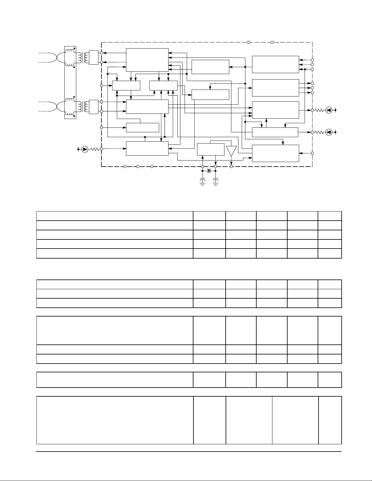
Balun
V
CC
TX+
Filter
TX–
Loop L
RX+
Filter
RX–
FULLD L
LNKFL H
TP Differential
Driver and Control
Loop Back
TP Differential Receiver
with Smart Squelch
Full Duplex Disable
Duplex Mode
Select
Link Fail Disable
TTL/CMOS
MC34055
Simplified Block Diagram
Driver Pre–Emphasis
Collision
Detect
Link Beat
Control
Jabber Disable
Transmit Idle
Collision Announcement
Link Pulse
Clock Oscillator
TTL/CMOS
Timer
Data In
Collision T est
Data Out
VCC (Dig/Ana)Pwr V
CC
Transmit Input
and Control
Received Data
Output and
Control
Collision
Detect
Outputs
Jabber
Signal
Quality
Error
CMOS
ECL
TTL/CMOS
TTL/CMOS
ECL
TTL/CMOS
TTL/CMOS
TTL/CMOS
TTL/CMOS
TX Data A
TX Data B
TX EN H
RX Data A
RX Data B
RX EN H
CTL H
JABB H
SQE EN L
V
CC
V
CC
Clk–Clk +
Clk
Out
*The sale and use of this product is licensed
*under technology covered by one or more
*Digital Equipment Corporation patents.
Ana.
Gnd
Dig.
Pwr
Gnd
Gnd
10MHz
This device contains 9,875 active transistors.
RECOMMENDED OPERATING CONDITIONS
Characteristic Symbol Min Typ Max Unit
Power Supply Voltage V
CC
Voltage Applied to Logic Inputs and Status Pins – 0 – 5.25 Vdc
Differential Input Voltage – 0.59 – 2.8 Vpp
Operating Ambient Temperature T
NOTE: All limits are not necessarily functional concurrently.
ELECTRICAL CHARACTERISTICS (0°C ≤ T
≤ 70°C, VCC = 5.0 V, unless otherwise noted.)
A
A
Characteristic Symbol Min Typ Max Unit
Supply Current (4.75 V ≤ VCC ≤ 5.25 V) I
CC
Reset Circuit Threshold – 4.0 – 4.4 Vdc
TWISTED PAIR TRANSMITTER
Output Differential V oltage
(See Load Circuits: Differential Load Circuit)
V
O
Output Differential Voltage with Pre–Emphasis 2.2 2.53 2.8
Output Differential V oltage 1.56 1.72 1.98
Common Mode Driver Impedance Z
Transmitter Differential Output Impedance Z
OCM
OD
TX DATA A
Input High Voltage (IIH = + 20 µA) V
Input Low Voltage (IIL = –150 µA) V
IH
IL
TX DATA B
Input Voltage (See Load Circuits: ECL Load Circuit)
High: @ 0°C V
IH
@ 25°C 0.984 VCC– 0.877 0.984 VCC– 0.727
@ 70°C 0.984 VCC– 0.825 0.984 VCC– 0.644
Low: @ 0°C V
IL
@ 25°C 0.750 VCC– 0.550 0.750 VCC– 0.350
@ 70°C 0.750 VCC– 0.531 0.750 VCC– 0.324
4.75 5.0 5.25 Vdc
0 – 70 °C
– 60 180 mA
6.0 8.5 14 Ω
8.0 15.5 29 Ω
3.15 – 5.25 Vdc
0 – 0.8
0.984 VCC– 0.923 0.984 VCC– 0.763
0.750 VCC– 0.568 0.750 VCC– 0.361
Vpp
Vdc
2
MOTOROLA ANALOG IC DEVICE DATA
Page 3
MC34055
ELECTRICAL CHARACTERISTICS (0°C ≤ T
Characteristic Symbol Min Typ Max Unit
TX EN H
Input High Voltage (IIH = 200 µA) V
Input Low Voltage (IIL = – 20 µA) V
RX DATA A/RX EN H/JABB H/CTL H
Output Voltage (See Load Circuits: CMOS Load Circuit)
High (IOH = –12 mA) V
Low (IOL = +16 mA) V
RX DATA B
Output Voltage (See Load Circuits: ECL Load Circuit)
High: @ 0°C V
@ 25°C 0.984 VCC– 0.877 0.984 VCC– 0.727
@ 70°C 0.984 VCC– 0.825 0.984 VCC– 0.644
Low: @ 0°C V
@ 25°C 0.750 VCC– 0.550 0.750 VCC– 0.350
@ 70°C 0.750 VCC– 0.531 0.750 VCC– 0.324
SIGNAL QUALITY ERROR TEST ENABLE CONTROL (SQE EN L)
Test Control Voltage
Test Disabled (Input High Voltage)(IIH = + 20 µA Max.) V
Test Enabled (Input Low Voltage)(– 50 µA < IIL < –150 µA) V
FULL DUPLEX MODE SELECT (FULLD L)
Mode Select Control Voltage
Normal Operation (Input High)(IIH = + 20 µA) V
Full Duplex (Input Low)(– 50 µA < IIH < –150 µA) V
LOOPBACK TEST MODE FUNCTION (LOOP L)
Test Control Voltage
Test Disabled (Input High)(IIH = + 20 µA) V
Test Enabled (Input Low)(IIL = – 200 µA) V
LINK FAIL STATUS (LINKFL H)
Status Output Voltage (See Load Circuits: CMOS Load Circuit)
Maximum Voltage for Output Low Condition (IOL = 20 mA) V
Output Low Sink Current V
CLOCK OSCILLATOR
Clk+ Input Logic Threshold
High Level Input Voltage (IIH = +100 µA Max.) V
Logic Low Input Voltage (IIL = –100 µA Max.) V
Clk Out Output Voltage (See Load Circuits: CMOS Load Circuit)
Logic High (IOH = –12 mA) V
Logic Low (I
= +16 µA) V
out
≤ 70°C, VCC = 5.0 V, unless otherwise noted.)
A
IH
IL
OH
OL
OH
OL
IH
IL
IH
IL
IH
IL
OH
OL
IH
IL
OH
OL
2.0 – 5.0 Vdc
0 – 0.8
Vdc
3.7 – –
– – 0.5
Vdc
0.984 VCC– 0.923 0.984 VCC– 0.763
0.750 VCC– 0.568 0.750 VCC– 0.361
Vdc
2.0 – 5.0
0 – 0.8
Vdc
2.0 – 5.0
0 – 0.8
Vdc
2.0 – 5.0
0 – 0.8
– – 0.5 Vdc
– – 20 mA
2.0 – 5.0 Vdc
– – 0.8 µA
Vdc
3.7 3.9 –
– 0.25 0.5
Ω
15 pF
ECL Load Circuit
330
MOTOROLA ANALOG IC DEVICE DATA
Output Load Circuits
20 pF
TTL/CMOS Load Circuit
6.0k
39 (1%)
TX–
Ω
39 (1%)
TX+
Differential Load Circuit
100
Ω
V
OD
3
Page 4
MC34055
TIMING CHARACTERISTICS
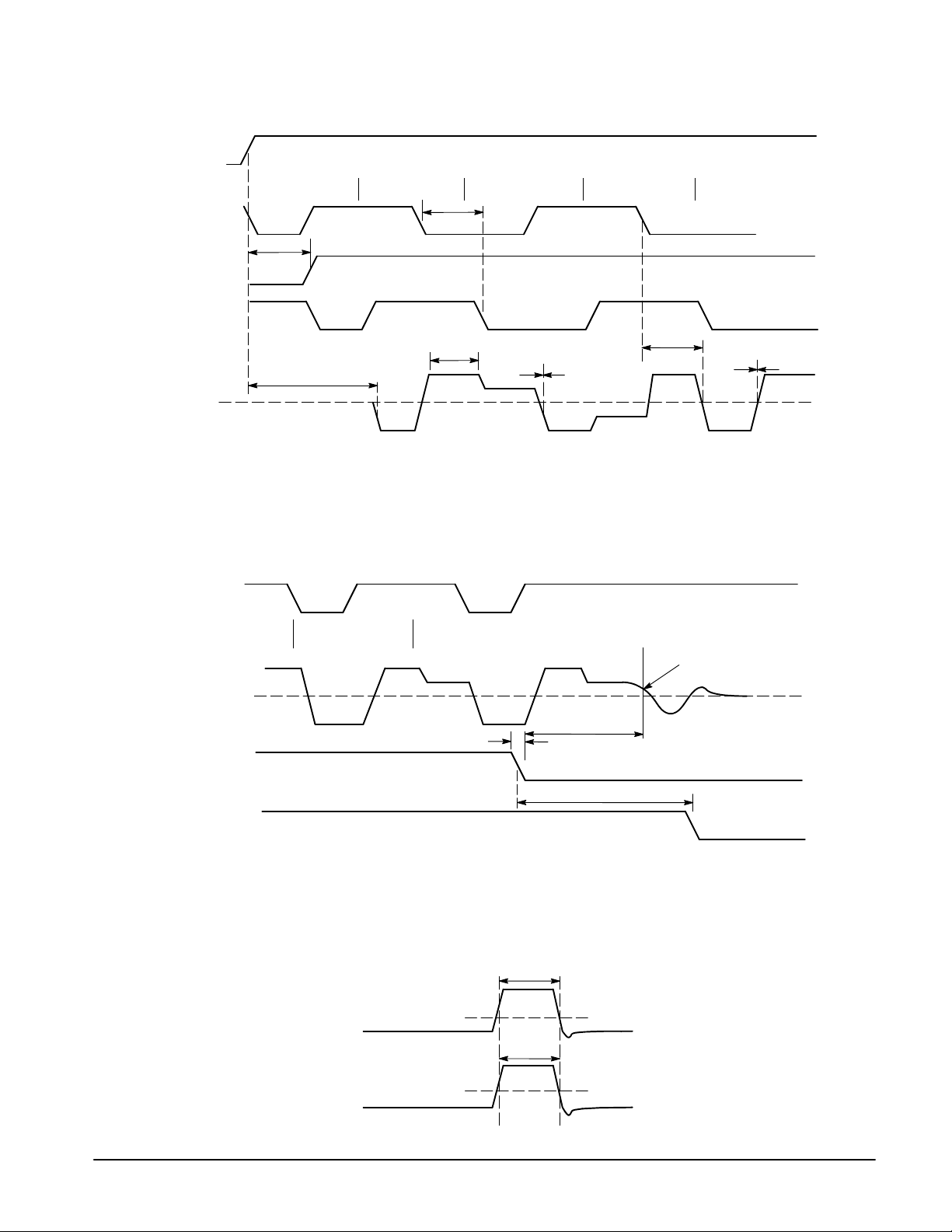
TRANSMIT START TIMING
TX EN H to TX+/TX– Enable Time t
TX Data A/B to TX+/TX– Enable Time t
Steady State Propagation Delay of TX Data A/B to TX+/TX– Output t
Pre–Emphasis Pulse Width t
Transmitter Caused Edge Skew Between TX+ and TX– t
Transmitter Added Edge Jitter to TX+/TX– from TX Data A/B t
Steady–State Delay between the TX Data A/B Input to the RX Data
A/B Outputs for Normal Operation
TX EN H Assert to RX EN H Assert Under Normal Operation t
TRANSMIT STOP TIMING
Delay between TX EN H Low and TX+/TX– High t
TX EN H Assert/De–assert Delay from TX EN H to RX EN H
Assert/De–assert
End of Packet Hold Time from Last TX Data A/B Edge or
TX EN H De–assert
LINK BEAT PULSES
Output Link Test Pulse Width t
Minimum Link Beat Pulse Duration on RX+/RX– t
LOOP BACK MODE TIMING
Delay from Loop L Deassertion to RX EN H Driven from
TX EN H Status
TX EN H Assert/De–assert to RX EN H, Assert/De–assert when in
Loop–Back Mode and Receiver Inactive
Steady–State TX Data A/B to RX Data A/B when in Loop–Back Mode t
SMART SQUELCH
Interval Unit Squelch Deactivation t
RECEIVE START TIMING
Receiver–Added Edge Skew to RX Data A/B Signal t
Receiver–Added Edge Jitter to RX Data A/B Signal t
Start–Up Delay from RX+/RX– to RX Data A/B t
Delay from RX EN H Assertion Until RX Data A/B Valid t
Steady–State Propagation Delay from RX+/RX– Data A/B t
RECEIVE SHUTDOWN TIMING
Last received Data Edge until the RX EN H Output forces low t
(0°C ≤ TA ≤ 70°C)
Characteristic
Symbol Min Typ Max Unit
TXEN
FDXD
TXSS
PRCM
Skew T
Jitter T
t
TXRX
DREL
TXDH
t
XTRE
t
TDDC
LKPW
LDCY_A
t
LTRA
t
LTRX
LTRD
SQ
Skew R
Jitter R
RXNE
RARE
RXSS
RXDE
– – 75 ns
– – 75 ns
– – 75 ns
45 – 55 ns
– – 2.0 ns
– – 4.0 ns
– – 50 ns
– – 50 ns
– – 75 ns
– – 400 ns
250 – – ns
80 – 120 ns
80 – 192 ns
– – 30 ns
– – 50 ns
– – 50 ns
– – 5.0 Bit
Times
– – 1.5 ns
– – 1.5 ns
– – 50 ns
–10 – +10 ns
– – 50 ns
155 – 250 ns
4
MOTOROLA ANALOG IC DEVICE DATA
Page 5
TX EN H
MC34055
Figure 1. Start Up and Steady State Transmit Timing
Bit Pattern
TX Data A/B
RX EN H
RX Data A/B
TX+/TX–
TX Data A/B
Bit Pattern
t
DREL
t
TXEN
t
TXRX
t
PRCM
t
SKEW T
Figure 2. Driver Shutdown Timing
01
0101
t
TXSS
t
JITTER T
TX+/TX–
TX EN H
RX EN H
RX+/RX–
TX+/TX–
t
TXDH
Figure 3. Link Pulse Timing
t
LDCY_A
t
LKPW
t
TDDC
t
585mV
XTRE
585mV
585mV
MOTOROLA ANALOG IC DEVICE DATA
5
Page 6

TX EN H
Bit Pattern
TX Data A/B
RX EN H
RX Data A/B
Loop L
MC34055
Figure 4. Loop Back Timing
t
LTRX
t
LTRA
t
LTRD
101
RX+/RX–
RX EN H
RX Data A/B
Figure 5. Receive Startup Timing
1010
t
SQ
Figure 6. Receive Shutdown Timing
t
t
SKEW R
t
RXNE
RARE
10
t
RXSS
t
JITTER R
6
RX+/RX–
RX EN H
t
RXDE
MOTOROLA ANALOG IC DEVICE DATA
Page 7

MC34055
PIN FUNCTION DESCRIPTION
Pin
1 Clk Out TTL/CMOS buffered 10 MHz clock output. This pin will source 400 µA and sink 16 mA.
2 TX Data A CMOS transmit input pin. Data input at this pin is output to the TP media. The input will source
3 TX Data B Raised ECL transmit input pin. Data input at this pin is output to the TP media. The input can
4 TX EN H TTL/CMOS transmit enable pin. Transmit is enabled when asserted high. The input will source
5 Dig. Gnd Digital ground
6 VCC(Dig/Ana) Digital and analog VCC. With the current consumed at this pin and Pin 18, the device will
7 Ana. Gnd Analog ground
8 RX Data A TTL/CMOS received data output pin. Data from the TP media is output at this pin. The output
9 RX Data B Raised ECL received data output pin. Data from the TP media is output at this pin.
10 RX EN H TTL/CMOS received data output enable pin. This pin is asserted after the Smart Squelch
11 Loop L TTL/CMOS Loopback test select. Asserting this pin causes the transmit data to be looped to
12 LNKFL H This pin is driven high to indicate a link fail state. When low, the pin will sink 20 mA to light an
13 JABB H TTL/CMOS Jabber status pin. This pin is asserted when a Jabber condition is detected and will
14 CTL H TTL/CMOS status pin. This pin pulled high when Jabber or Collision conditions are detected.
15 RX– The inverting terminal of the TP differential receiver.
16 RX+ The noninverting terminal of the TP differential receiver.
17 FULLD L TTL/CMOS duplex mode select. When low, this pin forces the device to operate in full–duplex
18 Pwr V
19 Pwr Gnd Power ground pin.
20 TX– The inverting terminal of the TP dif ferential driver.
21 TX+ The noninverting terminal of the TP differential driver.
22 SQE EN L TTL/CMOS Signal Quality Error test enable pin. Pulling this pin low allows test of the collision
23 Clk– TTL/CMOS clock oscillator pin. See Pin 24.
24 Clk+ TTL/CMOS clock oscillator pin. This pin is used with Pin 23 if the internal oscillator is to be free
Symbol Description
less than 175 µA and sink less than 20 µA.
source 40 µA for a high level input or 70 µA for a low level input.
less than 175 µA and sink less than 20 µA.
consume less than 180 mA at 5.0 Vdc.
will source 12 mA and sink 16 mA.
circuitry determines that there is valid data at the TP input pins and also when internal
loop–back is occurring. The output will source 12 mA and sink 16 mA. The receive data outputs
are forced high when this pin is low.
the receive circuit while the TP transmit driver sends a link pulse. The input will source less
than 175 µA and sink less than 20 µA.
LED. An usquelched condition due to valid data on the receive circuit will cause the pin to
transition high and low in 100 ms intervals.
source 12 mA and sink 16 mA.
Also high for a time interval when a Signal Quality Error test is being performed. The pin will
source 12 mA and sink 16 mA.
mode. The input will source less than 175 µA and sink less than 20 µA.
CC
Power supply pin. With the current consumed at this pin and Pin 6, the device will consume
less than 180 mA at 5.0 Vdc.
detect circuitry without affecting the twisted pair channel. The input will source less than 175 µA
and sink less than 20 µA.
run with a crystal. The oscillator can also be directly driven with a TTL/CMOS clock signal at
this pin. The oscillator frequency should be 10 MHz with a duty cycle of 50 ± 20%.
MOTOROLA ANALOG IC DEVICE DATA
7
Page 8

MC34055
FUNCTIONAL DESCRIPTION
Introduction
The Motorola 10BASE–T transceiver, designed to comply
with the ISO 8802–3[IEEE 802.3] 10BASE–T specification,
will support one Medium Dependent Interface (MDI) through
standard 10BASE–T filters and transformers. Although the
device is capable of being used in embedded or external
Medium Attachment Units (MAU), it was primarily designed
for use in repeater or hub applications. For this reason a
digital interface is provided rather than an AUI interface. This
interface is TTL, CMOS, and raised ECL compatible and
allows for easy connection in hub applications.
Other features of the MC34055 include: select mode pins
of forcing Loop–Back and Full–Duplex operation; a Signal
Quality Error pin for testing the collision detect circuitry
without affecting the twisted pair output; and LED drivers for
Link Integrity status; Collision detection; and Jabber
detection. An on chip oscillator, capable of receiving a clock
input or operating under crystal control, is also provided for
internal timing and driving a buffered clock output.
Data Transmission
For data intended for the twisted pair, the MC34055 has
two data inputs, TX Data A and TX Data B. TX Data A is
CMOS compatible and TX Data B is raised ECL compatible.
The inputs were not intended to be used simultaneously in a
single application and are internally logically combined. The
unused input should be disabled by connection to VCC.
When data transmission is intended, the MC34055
detects the first falling edge of the Manchester encoded
frame at the input being used, synchronizes the on chip
oscillator (Pins 23 and 24) and asserts the twisted pair driver
output to full differential amplitude within 25 ns if the driver
enable pin (TX EN H) is previously asserted. Also, since
twisted pair attenuates a 10 MHz signal more than a 5.0 MHz
signal the 10BASE–T standard requires that data applied to
the twisted pair receive pre–equalization. To fulfill this
requirement the MC34055 provides an additional 730 mV for
approximately 50 ns to output data. This is accomplished
over the single pair of differential driver pins. TX+ and TX–,
and effectively equalizes the power of all data components at
the receiver. Figure 7A shows a 10 MHz waveform. Figure 7B
shows the effect of pre–emphasis on a 5.0 MHz waveform.
Manchester encoded data with the pattern shown in Figure
7A would represent a repeating pattern of zeros (000000...).
Figure 7B would represent an alternating pattern of ones and
zeros (0101010...).
Bit Pattern
TX+
Pin 21
TX–
Pin 20
Bit Pattern
Pin 21
TX+
1.25 V
1.25 V
0 V
Figure 7A. 10 MHz Waveform on Differential Outputs
000 000
p–p
p–p
Figure 7B. 5.0 MHz Waveform on Differential Outputs
0
1.25 V
p–p
0.885 V
p–p
50 ns
0 V
0 V
0101
0 V
0.50 ns
1.25 V
p–p
0.885 V
p–p
MOTOROLA ANALOG IC DEVICE DATA
TX–
Pin 20
8
Page 9

MC34055
The figures show the voltage waveforms on the differential
driver output pins. To actually meet the 10BASE–T
specification requires bandpass filtering and a pulse
transformer.
The output voltage waveform specifications of the IEEE
802.3 standard require that voltages impressed on the
twisted pair meet a voltage template. The MC34055 can
meet the voltage template for all the 10BASE–T applications
Figure 8. Differential Driver Media Interface Circuitry
TX+
+1
–1
Where: ZOD is the transmitters differential output impedance (~20 Ω),
Where: RS is a 1% series resistor,
Where: ZF is the filters impedance, and ZO is the characteristic
Where: impedance of the twisted pair (100 Ω).
ZOD/2
ZOD/2
20
21
TX–
R
S
R
S
by choosing the appropriate low pass filter and external
components in the driver output circuitry. When the
differential transmit driver output pins are configured to drive
the bandpass filters and pulse transformer as shown in
Figure 8, the resultant waveform is capable of meeting the
voltage template.
Following the end–of–frame activity, an internal pull–up
resistor pulls TX Data A/B high and causes the differential
driver to maintain full differential output voltage for
approximately 250 ns. The differential driver interprets the
lack of transition activity as an end of frame and starts an idle
timer. Should another frame intended for the twisted pair
arrive before the idle timer expires(~250 ns), the idle timer
will be reset, if not, the transmit driver function will begin the
decay to idle process. During idle periods the differential
driver must force the media to a minimal differential voltage
unless a link beat is being produced. The transition to
minimal voltage is subject to performance requirements in
the IEEE specification and is met by the MC34055 when the
appropriate filters and transformers are used to interface to
the media.
The MC34055 differential driver generates link pulses
(beats) during idle periods. The link pulses produced are
singular positive (TX+ positive with respect to TX–) pulses
applied to the media at 16 ms intervals and last
approximately 100 ns. The link pulses allow the receiver at
the other end of the link to verify the validity of the segment.
There is the possibility, due to the two asynchronous
sources, that one of the two input pins (TX Data A or TX Data
B) will receive frame activity immediately after a link pulse is
initiated. In this event, the transmit differential driver will
remain active for the entire frame interval and the link pulse
will not affect more than one bit interval.
The MC34055 also has Jabber circuitry to detect and
disable the twisted pair driver in the event that a serial
controller fails constantly transmitting. Should any data
source try to transmit longer than 20 ms minimum, the Jabber
function will disable the differential driver outputs, the
Pulse
Transformer
Z
F
Z
O
Z
F
Twisted Pair
collision presence detector and the internal loopback
function. Also, two status indicator pins, CTL H and JABB H
are asserted. The MC34055 will remain in the jabber state
until the TX EN H pin is pulled low or the jabbering input
ceases to toggle for a minimum of 500 ms. The status
indicator pins, CTL H and JABB H will also sink up to 20 mA
and can therefore support external LEDs.
The driver also works with the receiver to provide
loop–back. Under normal operating conditions (Loop L= “1”),
the data applied to the TX Data A/B pins is looped back
internally to the RX Data A/B pins. This function is disabled
when there is a collision condition or FULLD L is low.
Data Reception
Data intended for the DTE proceeds from the twisted pair
to the isolation transformer and bandpass filters before
reaching the differential receiver terminals. Figure 9 shows
the configuration of the external media receive circuitry . Once
transitions at the receiver terminals (RX+ and RX–) are
detected, the on–chip oscillator is synchronized and the
received data is screened by smart squelch circuitry for
validity. This qualification requires incoming data to meet
amplitude and sequence requirements. If the data meets the
Smart Squelch requirements, the receiver enters the
unsquelch state and the data is forwarded to the RX Data A/B
output pins provided Loop L is not low. Two data outputs are
provided to increase design flexibility, RX Data A and RX
Data B. RX Data A is CMOS/TTL compatible and RX Data B
is raised ECL compatible.
MOTOROLA ANALOG IC DEVICE DATA
9
Page 10

MC34055
Figure 9. Differential Receiver Media Interface Circuitry
Pulse
Transformer
Z
Twisted Pair
Z
O
Where: RT is a terminating resistor (100 Ω),
Where: ZF is the filters impedance, and ZO is the
Where: characteristic impedance of the twisted pair (100 Ω).
F
R
T
Z
F
15
16
RX–
RX+
The MC34055 powers up in a squelched and “link OK”
state, after which minimum and maximum link test and
maximum link fail timers are started. If valid data or a link
pulse is received after the link test minimum timer but before
the link fail maximum timer times out, the timers are reset and
begin counting again. In the event of missing or incorrect link
pulses, the MC34055 enters the link fail state whereby the
LNKFL H status pin is asserted until valid data or link pulse
activity appears at the receiver terminals.
Powering up in the squelched state assures that the data
path to the data output pin (RX Data A/B) is disabled, and
prevents noise at the receiver terminals (RX+/RX–), from
being interpreted as valid input data. Once transitions appear
at the receiver terminals, the smart squelch circuitry checks
for the smart squelch requirements to unsquelch; an
alternating sequence (1010... or 0101...) of pulses with
amplitude of at least 525 mV. This requirement is met by the
preamble of an IEEE 802.3 frame with good signal to noise
ratio.
After a pulse is received and checked for proper polarity
and amplitude, the pulse width is checked for proper
duration. If the duration is to short or too long the smart
squelch circuitry resets and begins to look again for a proper
sequence. By requiring the differential pulses to meet
amplitude and sequence requirements, it is unlikely that
pulses due to crosstalk from coresident twisted pairs are
capable of causing the receiver to unsquelch. If a positive
pulse is received first and the differential driver is not
transmitting, the receiver should unsquelch after three
alternating pulses. If a negative pulse is received first, one
additional pulse is required before unsquelch. If the
differential driver is transmitting, three additional pulses are
required to unsquelch.
After meeting the smart squelch requirements, the
MC34055 will pull high the RX EN H pin and enable the path
to the receive data pin (RX Data A/B) provided the MC34055
is not in the loop back test mode (Loop L low). If the receiver
unsquelches, the receive enable pin remains high and the
data path to the receive data pin remains enabled until
transitions cease to exist at the receiver terminals. V alid data
reception is also indicated by high/low transitions of the
LNKFL H pin at 100 ms intervals. When transitions at the
differential terminals cease, marking the end of frame activity ,
the receiver re–enters the squelch state, pulls low on the RX
EN H pin, and begins accepting valid link pulses until the start
of the next 802.3 frame.
If the MC34055 is requested to begin transmitting (TX EN
H is asserted), and the receiver unsquelches simultaneously,
there is a collision. Also, if the MC34055 driver enable pin is
previously asserted and the receiver detects valid transition
activity, the receiver Smart Squelch circuitry verifies the
possibility of collision by requiring three extra transitions at
the differential receiver before the unsquelch condition is
reached. If unsquelch occurs, a collision condition exists.
During all collision conditions the MC34055 asserts the CTL
H status pin for the duration of the condition and for a time
after the end of collision.
During a collision condition the receive and transmit paths
are still both enabled allowing transparency to the media.
Either the presence of simultaneous transmit and receive
activity or the condition of the CTL H status pin can be used
by the communications controller to acknowledge and react
to the collision. In applications where a 10 MHz collision
signal is required by an SIA, the combination of this status pin
and the clock oscillator output can be logically combined to
provide a 10 MHz output. If the DTE reacts to the collision
and ceases transmitting, the MC34055 will decay to idle until
a re–transmit is attempted.
Crystal Oscillator
The MC34055 has an on–chip clock oscillator used to
provide a reliable and accurate time reference to all the
internal timers. The oscillator can be run with a crystal or
driven at Pin 24 from an external clock source. Also provided
is a buffered clock output which is useful if the MC34055 is to
be used in a repeater or concentrator application.
10
T able 1. The crystal used in the oscillator is subject to the following specifications.
Crystal Operating Mode Fundamental
Crystal Cut Type AT
Crystal External Shunt Capacitance 7.0 pF Max
Crystal Resonant Mode Series
Crystal Accuracy ± 0.01% @ 25°C
Crystal Temperature Variance 0.005% from 0° to 70°C
Crystal Series Resistance 25 Ω Max, 17 Ω Typical
Crystal Operating Temperature Range 0° to 70°C
MOTOROLA ANALOG IC DEVICE DATA
Page 11

MC34055
LOOP L Test Mode
If the Loop L pin is low, the MC34055 is in a test mode
whereby the data at the input pin (TX Data A/B) is being
looped back internally to the receive data pin(RX Data A/B).
In this mode the data path from the differential receiver
terminals to the receive data output pins (RX Data A/B) is
disconnected while the Smart Squelch functionality of the
differential receiver is still operational. This test mode allows
the DTE to test the MC34055 internal loop back circuitry
since the data is looped back to the receive circuitry as close
to the twisted pair interface as possible.
Signal Quality Error Test
The MC34055 also provides the ability to test the collision
detect circuitry without disabling either of the data paths. By
pulling the SQE EN L pin low, a collision test is provided to
the collision detect circuitry immediately following the last
edge of a transmitted 802.3 frame. The test verifies the
operability of the collision detect circuitry, operability is
announced by the assertion of the CTL H pin for a period
following a valid data transmission.
Jabber Detection
The transmit circuitry of the MC34055 has the ability to
monitor and shut down the differential driver in the event of a
jabber condition. If transmission activity ever exceeds 20 ms
minimum, the differential driver, the collision detect, and
internal loop back circuits are disabled. To announce the
presence of a jabber condition, both the CTL H and the JABB
H status output pins are asserted. In order to end the jabber
condition, the TX Data A/B input must stop toggling, or the TX
EN H pin must be pulled low for a minimum of 500 ms. The
status output pins have the ability to drive an external led and
were added to facilitize network manageability. The jabber
status outputs will not assert during power up or power down.
Full Duplex Mode
The MC34055 can be operated in a full–duplex mode if
required. When the FULLD L pin is pulled low the device will
enter the full duplex mode. This mode allows the transmitter
and driver to operate independently. Collision will not be
announced and the internal loop back operation is disabled.
The Signal Quality Error test, however, is still operational if
enabled.
Status Pins
The MC34055 has three status indicator pins capable of
sourcing or sinking enough current to support an external
LED. Status pin levels (“1” or “0”) report the condition of the
transceiver. Table 2 shows the combinations and
significance.
T able 2
Status Pin
JABB H CTL H LNKFL H
“0” “1” X Collision condition or Signal Quality Error test.
“1” “1” X Jabber condition
X X “0” Link Failure. Incorrect or nonexistent link pulses, or lack of data at the
X X “1” Link “OK”. Receiving link pulses.
X X “0101…” Link “OK”. Receiving valid data.
receiver terminals.
T est Select Pins
The MC34055 has three operation mode test select pins,
Loop L, SQE EN L and FULLD L. The level of the pin
determines the mode of operation. Table 3 shows the levels
and corresponding conditions of the status pins.
T able 3
Pin Status Condition
Loop L
SQE EN L
FULLD L
“1” Normal operating mode. Loop back occurs when the transmitter initiates and the receiver is receiving
link pulses. The RX EN H pin follows the TX EN H pin and the transmit data appears on the RX Data
A/B output pin being used.
“0” Loop back test mode. The transmit circuit is looped back internally as close to the differential receive
circuit as possible. In this mode the RX EN H pin follows the TX EN H pin and the transmit data appears on the RX Data A/B output pin being used. Any received data other than link pulses are ignored
and the receiver will not unsquelch or announce collision.
“0” Normal operating mode. Concurrent transmit and receive activity results in a collision condition.
“1” Test enabled. An internal test is run on the collision circuitry and the CTL H pin is asserted for a time
window following the last positive packet edge. Data transmission and reception is undisturbed.
“1” Normal operating mode. Internal loop–back is operable and collision is announced.
“0” Internal loop–back is disabled and collision will not be announced. Signal Quality Error test is
still operable.
Condition
MOTOROLA ANALOG IC DEVICE DATA
11
Page 12

MC34055
APPLICATIONS INFORMATION
The MC34055 implements the physical layer of a
10BASE–T application of IEEE 802.3. It provides the
physical connection to the media (twisted pair) and the
services required by the MAC sublayer of the Data Link
Layer. Two interfaces are defined in the IEEE 802.3
specification of the physical layer; one is the MDI providing
connection to the twisted pair; and the other is the AUI
providing connection to the encoder/decoder function of the
Data Link Layer. While the MC34055 provides the connection
to the twisted pair, a CMOS and raised ECL interface is
provided instead of an AUI.
The MC34055 implements the twisted pair interface of the
physical layer in a 802.3 10BASE–T application but circuitry
must be added if an AUI is desired, (see Figure 10 for
suggested schematic). For example, an external MAU
application requires the AUI and a twisted pair interface. A
chip capable of realizing the AUI interface is the Texas
Instruments SN75ALS085. This IC has an AUI interface and
another interface which is compatible with the MC34055. The
differential input of the 75ALS085 can be used for the
TX+/TX– terminals of the AUI. The differential drivers of the
75ASL085 can be used as the RX+/RX– and the
COL+/COL– terminals of the AUI. The other interface of the
75ALS085 then will interface to the MC34055 by three paths
shown in the application suggestion. The application
accounts for all the inputs/outputs of an external MAU.
Embedded applications do not require a full AUI and a
MC10116 can be used to interface between the raised ECL
interfaces of the MC34055 and the AUI of existing
encoder/decoder chips. The MC10116 is a MECL 10k Triple
Line Receiver with typical propagation delay and rise and fall
times (20% to 80%) of 2.0 ns. Figure 1 1 shows the use of the
MC10116 with the MC34055 and the AMD 7992 SIA.
In a multi–port repeater , or hub, a port is required for each
DTE connected to the IEEE 802.3 network. This port consists
of two connections, one for the TX+/TX– pair and another for
the RX+/RX– pair. The repeater unit then multiplexes these
lines so that all of the stations are capable of transmitting to
or receiving from all the other stations on the network. This
establishes the need for a transceiver without an AUI
interface. If an AUI is present with each 10BASE–T
transceiver, chip count is increased because there is a
requirement to convert from balanced to unbalanced lines
before multiplexing.
An application suggestion for the use of the MC34055
used in a multiport repeater is shown in Figure 6. Here the
receive and transmit lines for the 10BASE–T transceivers are
multiplexed by the hub hardware.
12
MOTOROLA ANALOG IC DEVICE DATA
Page 13

MC34055
AUI
+5.0
0.1
0.1
+5.0
10
V
CC
V
CC
+5.0
4.7 k
Loop1
4.7 k
RX O1 Loop2
4.7 k
+5.0
+5.0
RX I1
RX
RX I1
RX EN1
39.339.3
0.1
AUI Chip
TX I1
TX O1
75ALS085
NC
TX
TX O1
TX EN1
TX EN2
COL
TX O2
+5.0
TX O2
TX I2
180
NC
270
Gnd
Gnd
Gnd
Gnd
RX EN2
RX O2
RX I2
RX I2
820
NC
Figure 10. External MAU Application
+5.0
0.11010
10
1.0
VCCPwr
VCC(Dig/Ana)
Balun
Twisted Pair
39
TX Data A
TX+
TX Data B
TX–
Filter
4.7 k
39
TX EN H
RX Data B
MC34055
RX+
100
Filter
RX–
CLK
OUT
PWR Gnd
ANA Gnd
DIG Gnd
CLK–
CLK+
20 20
10 MHz
4.7 k
+5.0
470
CTL H
Loop L
LNKFL H
+5.0
RX EN H
RX Data A
Full D
470
JABB H
SQE EN L
MOTOROLA ANALOG IC DEVICE DATA
13
Page 14

MC34055
TCLK
TX+
TDATA
TX–
TENA
I
S
A
MC10116
L
RX+
ANC
RCLK
RX–
E
AM7990
RDATA
RENA
CLSN
AM7992
COLL–
COLL+
Figure 11. Internal MAU Application
+5.0
0.1
1.0
10
VCCPwr
VCC(Dig/Ana)
10
Balun
Twisted Pair
39
TX Data A
TX+
+5.0
4.7 k
TX Data B
TX–
39
Filter
TX EN H
RX Data B
MC34055
RX+
100
Filter
RX–
NC
NC
CLK
OUT
PWR Gnd
ANA Gnd
DIG Gnd
CLK–
CLK+
20 20
10 MHz
4.7 k
+5.0
470
CTL H
Loop L
LNKFL H
+5.0
RX EN H
RX Data A
Full D
470
JABB H
SQE EN L
14
MOTOROLA ANALOG IC DEVICE DATA
Page 15

MC34055
AUI
0
TX EN B
0
RX EN B
TX Data B
COL
TX
RX
39.339.3
0.1
Hub
Hardware
0
0
RX Data B
7
RX EN B
7
TX EN B
RX Data B
7
7
TX Data B
Figure 12. 10BASE–T Connecentrator Application
Balun
RX–
Filter
MC34055
RX+
TX–
TX+
Filter
00000000
Other
MC34055
Balun
RX–
RX+
Filter
MC34055
TX–
TX+
Filter
MOTOROLA ANALOG IC DEVICE DATA
15
Page 16

–T–
SEATING
PLANE
MC34055
OUTLINE DIMENSIONS
DW SUFFIX
PLASTIC PACKAGE
CASE 751E–04
(SO–24L)
–A–
24 13
–B–
P 12 PL
M
M M
B
0.010 (0.25)
112
D 24 PL
0.010 (0.25) A B
M
T
S S
J
F
C
G 22 PL
K
R X 45°
NOTES:
1. DIMENSIONING AND TOLERANCING PER ANSI
Y14.5M, 1982.
2. CONTROLLING DIMENSION: MILLIMETER.
3. DIMENSIONS A AND B DO NOT INCLUDE
MOLD PROTRUSION.
4. MAXIMUM MOLD PROTRUSION 0.15 (0.006)
PER SIDE.
5. DIMENSION D DOES NOT INCLUDE DAMBAR
PROTRUSION. ALLOWABLE DAMBAR
PROTRUSION SHALL BE 0.13 (0.005) TOTAL IN
EXCESS OF D DIMENSION AT MAXIMUM
MATERIAL CONDITION.
MILLIMETERS INCHES
MIN MINMAX MAX
DIM
A
B
C
D
F
G
J
K
M
P
R
15.54
7.60
2.65
0.49
0.90
0.32
0.29
8
10.55
0.75
0.601
0.292
0.093
0.014
0.016
0.009
0.005
0
°
°
0.395
0.010
15.25
7.40
2.35
0.35
0.41
1.27 BSC 0.050 BSC
0.23
0.13
0
°
10.05
0.25
0.612
0.299
0.104
0.019
0.035
0.013
0.011
8
°
0.415
0.029
Motorola reserves the right to make changes without further notice to any products herein. Motorola makes no warranty , representation or guarantee regarding
the suitability of its products for any particular purpose, nor does Motorola assume any liability arising out of the application or use of any product or circuit, and
specifically disclaims any and all liability, including without limitation consequential or incidental damages. “T ypical” parameters which may be provided in Motorola
data sheets and/or specifications can and do vary in different applications and actual performance may vary over time. All operating parameters, including “Typicals”
must be validated for each customer application by customer’s technical experts. Motorola does not convey any license under its patent rights nor the rights of
others. Motorola products are not designed, intended, or authorized for use as components in systems intended for surgical implant into the body, or other
applications intended to support or sustain life, or for any other application in which the failure of the Motorola product could create a situation where personal injury
or death may occur. Should Buyer purchase or use Motorola products for any such unintended or unauthorized application, Buyer shall indemnify and hold Motorola
and its officers, employees, subsidiaries, affiliates, and distributors harmless against all claims, costs, damages, and expenses, and reasonable attorney fees
arising out of, directly or indirectly, any claim of personal injury or death associated with such unintended or unauthorized use, even if such claim alleges that
Motorola was negligent regarding the design or manufacture of the part. Motorola and are registered trademarks of Motorola, Inc. Motorola, Inc. is an Equal
Opportunity/Affirmative Action Employer.
How to reach us:
USA/EUROPE/ Locations Not Listed: Motorola Literature Distribution; JAPAN: Nippon Motorola Ltd.; Tatsumi–SPD–JLDC, 6F Seibu–Butsuryu–Center,
P.O. Box 20912; Phoenix, Arizona 85036. 1–800–441–2447 or 602–303–5454 3–14–2 Tatsumi Koto–Ku, Tokyo 135, Japan. 03–81–3521–8315
MFAX: RMF AX0@email.sps.mot.com – TOUCHT ONE 602–244–6609 ASIA/PACIFIC: Motorola Semiconductors H.K. Ltd.; 8B Tai Ping Industrial Park,
INTERNET: http://Design–NET.com 51 Ting Kok Road, Tai Po, N.T., Hong Kong. 852–26629298
16
◊
MOTOROLA ANALOG IC DEVICE DATA
MC34055/D
*MC34055/D*
 Loading...