

Page 1
MC34018 LINEAR INTEGRATED CIRCUIT
VOICE SWITCHED SPEAKERPHONE CIRCUIT
DESCRIPTION
The Contek MC34018 speaker-phone integrated circuit
incorporates the necessary functions to produce a high quality
hands-free speaker-phone system. The applications include
household and office speaker-phones, intercom systems,
hand free kit for mobile phones, and others.
FEATURES
*All necessary level detection and attenuation controls for a
hand-free telephone included.
*Background noise level monitoring with long time constant.
*Background sound level compensation for transmit and
receive levels as well as the background level.
*Wide operating dynamic range through signal compression.
*On-chip voltage regulators illuminate external regulators for
lining operation.
*Power audio amplifier for typical 100mW output (into 25
ohms)with peak limiting for speaker to minimize distortion.
*Chip Select pin for active/stand by operation.
*Volume control function for external volume control.
*Standard 28-pin plastic DIP and SOP package.
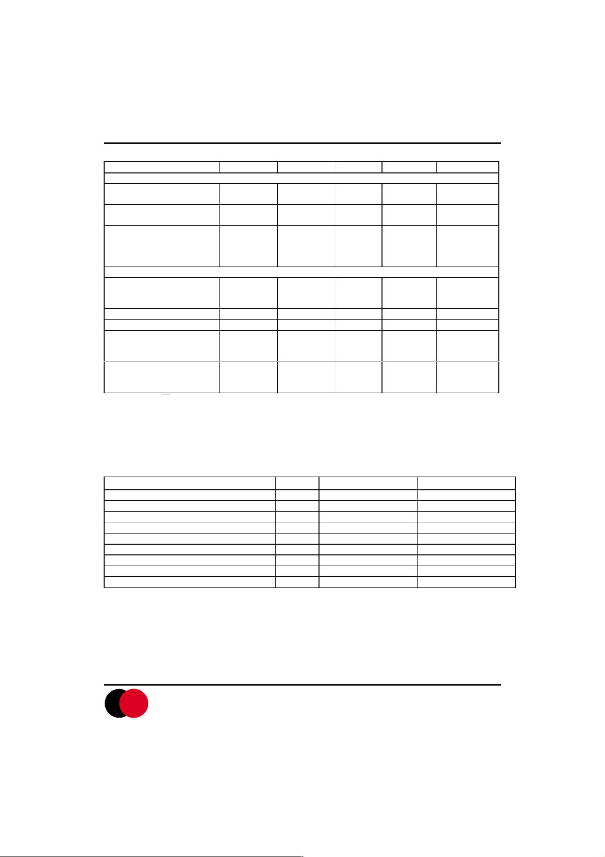
ABSOLUTE MAXIMUM RATINGS(Ta=25 C,Voltages referred to pin 22)
PARAMETER VALUE UNIT
V+ terminal Voltage (pin 16) +12,-1.0 V
CS
(pin 18)
Speaker amplifier Ground(pin 14) +3.0,-1.0 V
VLC(pin 24) +VCC,-1.0 V
Storage temperature -65 ~ +150 C
+12,-1.0 V
SOP-28
DIP-28
RECOMMENDED OPERATION CONDITIONS
PARAMETER VALUE UNIT
V+ Terminal Voltage (pin 16) +6.0 to +11 V
CS
(pin 18)
Icc(pin 20) 0 to 3.0 mA
VLC(pin 24) 0.55VB to VB V
Receive Signal(pin 27) 0 to 250 mVrms
Microphone Signal(pin 9) 0 to 5.0 mVrms
Speaker Amplifier Ground (pin 14) -10 to +10 mVdc
Ambient Temperature -20 to +60 C
0to+11 V
Contek Microelectronics Co.,Ltd.
CONTEK
http://www.contek-ic.com E-mail:sales@contek-ic.com
1
Page 2
MC34018 LINEAR INTEGRATED CIRCUIT
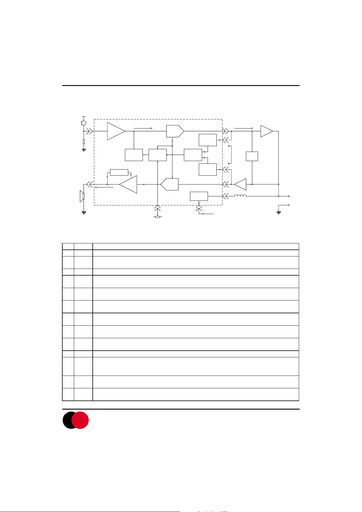
BLOCK DIAGRAM
MIC
SPEAKER
Contek
RECEIVE
CHANNEL
MIC AMP
PEAK LIMITER
SIGNAL/NOISE
DETECTOR
SPEAKER
AMP
TRANSMIT
CHANNEL
ATTENUATOR
CONTROL
RECEIVE VOLUME CONTROL
TRANSMIT
ATTENUATOR
RECEIVE
ATTENUATOR
TRANSMIT/
RECEIVE
COMPARATOR
REGULATOR
TRANSMIT LEVEL
DETECTOR
RECEIVE LEVEL
DETECTOR
VCC
ENABLEINPUT
SIDE
TONE
TRANSMIT
OUTPUT
DC INPUT
SIDE TONE
NETWORK
RECEIVEINPUT
TELEPHONE
LINE
PIN CONFIGURATIONS
PIN NAME DESCRIPTION
1 RR A resistor to ground provides a reference current for the transmit and receive attenuators
2 RTX A resistor to ground determines the nominal gain of the transmit attenuator ,the transmit channel gain
3 TXI Input to the transmit attenuator. Input resistance is nominally 5.0k ohms.
4 TXO Output of the transmit attenuator. The TXO output signal drivers the input of transmit level detcetor, as
5 TLI Input of the transmit level detector. An external resistor ac coupled to The TLI pin sets the detection
6 TLO Output of the transmit level detector. The external resistor and capacitor set the time the comparator
7 RLI Input of the receive level detector. An external resistor ac coupled to The RLI pin sets the detection
8 RLO Output of the receive level detector. The external resistor and capacitor set the time the comparator
9 MCI Microphone amplifier input. Input impedance is nominally 10k ohms and the dc bias voltage is
10 MCO Microphone amplifier output. The MIC amp gain is internally set at 34dB(50V/V).
11 CP1 A parallel resistor and capacitor connected between this pin and VCC holds a voltage corresponding
12 CP2 A capacitor at this pin peak detects the speech signals for comparison with the background noise level
13 XDI Input to the transmit detector system. The microphone amplifier output is ac coupled to the XDI pin
is inversely proportional to RTX resistance.
well as the external circuit which drivers the telephone line.
level. Decreasing this resistor increases the sensitivity to transmit channel signals.
will hold the system in the transmit mode after speech ceases.
level. Decreasing this resistor increases the sensitivity to receive channel signals.
will hold the system in the receive mode after speech ceases.
approximately equal to VB
to the background noise level. The transmit detector compares the CP1 voltage with the speech signal
from CP2.
held at CP1.
through an external resistor.
CONTEK
Contek Microelectronics Co.,Ltd.
http://www.contek-ic.com E-mail:sales@contek-ic.com
2
Page 3
MC34018 LINEAR INTEGRATED CIRCUIT
(continued)
PIN NAME DESCRIPTION
14 SKG High current ground pin for the speaker amplifier output stage. The SKG voltage should be within
10mV of the ground voltage at pin 22.
15 SKO Speaker amplifier output. The SKO pin will source and sink up to 100mA when ac coupled to the
speaker. The speaker amplifier gain is internally set at 34dB(50V/V).
16 V+ Input DC supply voltage. V+ can be powered from Tip and Ring if an ac decoupling inductor is used to
prevent loading ac line signals. The required V+ voltage is 6.0V to 11V(7.5V nominal ) at 7.0mA.
17 AGC A capacitor from this pin to VB stabilizes the speaker amplifier gain control loop, and additionally
controls the attack and decay time of this circuit. The gain control loop limits the speaker amplifier
input to prevent clipping at SKO. The internal resistance at AGC pin is nominally 110k ohms.
CS
18
19 SKI Input to the speaker amplifier. Input impedance is nominally 20k ohms.
20 VCC A 5.4V regulated output which powers all circuits except the speaker amplifier output stage. VCC can
21 VB An output voltage equal to approximately VCC/2 which series as an analog ground for the
22 GND Ground pin for the IC(except the speaker amplifier)
23 XDC Transmit detector output. A resistor and capacitor at his pin hold the system in the transmit mode
24 VLC Volume control input>connecting this pin to the slider of a variable resistor provides receive mode
25 ACF Attenuator control filter. A capacitor connected to this pin reduces noise transient as the attenuator
26 RXO Output of the receive attenuator. Normally this pin is ac coupled to the input of the speaker amplifier.
27 RXI Input of the receive attenuator. Input impedance is nominally is 5.0k ohms.
28 RRX A resistor to ground determines the nominal gain of the receive attenuator. The receive channel gain
Digital chip select input. When at a logic "0" (<0.7V) the VCC regulator is enabled. When at a logic "1"
(>1.6V),the chip is in the standby mode drawing 0.5mA.An open
is nominally 140k ohms. The input voltage should not exceed 11V.
be used to power external circuitry such as a microprocessor(3.0mA max.) A filter capacitor is
required.TheContek MC34018 can be powered by a separate regulated supply by connecting V+ and
VCC to a voltage between 4.5V and 6.5V while maintaining
speakerphone system. Up to 1.5mA of external load current may be sourced from VB. Output
impedance is 250 ohms. A filter capacitor is required.
during pauses between words or phrases. When the XDC pin voltage decays to ground, the
attenuators switch from the transmit mode to idle mode. The internal resistor at XDC is nominally 2.6k
ohms(see fig.1).
volume control. The VLC pin voltage should be less than or equal to VB.
control switches level of attenuation.
is directly proportional to the RRX resistance.
CS
pin is a logic "0".Input impedance
CS
at a logic "1".
ELECTRICAL CHARACTERISTICS(referred to fig. 1)
PARAMETER SYMBOL MIN TYP MAX UNIT
SUPPLY VOLTAGES
V+ Supply Current
V+=11V,Pin 18=0.7V
V+=11V,Pin 18=1.6V
VCC Voltage(V+=7.5V)
Line
Regulation(6.5V<V+<11V)
Output Resistance(I
Dropout Voltage(V+=5.0V)
VB Voltage(V+=7.5V)
Output Resistance(I
CC=3mA)
B=1.7mA)
IV+
Vcc
DVcc
RoVcc
Vccsat
Vb
Rovb
4.9 5.4
LN
2.5 2.9
Contek Microelectronics Co.,Ltd.
CONTEK
http://www.contek-ic.com E-mail:sales@contek-ic.com
65
6.0
80
250
9.0
800
5.9
150
20
300
3.3 Vdc
mA
mA
Vdc
mV
ohms
mV
ohms
3
Page 4
MC34018 LINEAR INTEGRATED CIRCUIT
(continued)
PARAMETER SYMBOL MIN TYP MAX UNIT
ATTENUATORS
Receive Attenuator Gain(1.0kHz)
Rx Mode, Pin 24= VB, Pin 27 =
250Mvrms
Range (Rx to Tx Modes)
Idle Mode, Pin 27= 250mVrms
RXO Voltage (Rx Mode) VRXO 1.8 2.3 3.2 mV
Delta RXO Voltage (Switch from Rx
to Tx Mode)
RXO Sink Current (Rx mode) IRXOL 75 mA
RXO Source Current (Rx mode) IROXH 1.0 3.0 mA
RXI Input Resistance RRXI 3.5 5.0 8.0 kW
Volume Control Range (Rx
Attenuator Gain, Rx Mode,
0.6VB<Pin 24<VB
ATTENUATORS
Transmit Attenuator Gain (1.0kHz)
Tx Mode, Pin 3 = 250mVrms
Range, (Tx to Rx Mode)
Idle Mode, Pin 3 = 250Mvrms
TXO Voltage (Tx mode) VTXO 1.8 2.3 3.2 Vdc
Delta TXO Voltage (switch from Tc
to Rx Mode)
TXO Sink Current (Tx mode) ITXOL 75 mA
TXO Source Current (Tx mode) ITXOH 1.0 3.0 mA
TXO Input Resistance RTXI 3.5 5.0 8.0 kW
ACF Voltage (VCC-Pin 25 Voltage)
Rx Mode
Tx Mode
Idle Mode
SPEAKER AMPLIFIER
Speaker Amp Gain (pin 19 =
20mVrms)
SKI Input Resistance RSKI 15 22 37 kW
SKO Voltage ( Pin 19 =Cap couple
to GND)
SKO High Voltage ( Pin 19 = 0.1V,
-100mA Load at Pin 15)
SKO Low Voltage (pin 19=0.1V,
+100mA Load at Pin 15)
MICROPHONE AMPLIFIER
Microphone Amp Gain ( Pin 9 =
10mVrms,1KHz)
Microphone Amp Input Resistance RMCI 6.5 10 16 kW
G
RX
DGRX
GRI
DVRXO 100 mV
CR 24.5 32.5 dB
V
G
TX
DGTX
GTXI
DVTXO 100 mV
DV
ACF
GSPK 33 34 35 dB
VSKO 2.4 3.0 3.6 Vdc
VSKOH 5.5 Vdc
VSKOL 600 mV
GMCI 32.5 34 35 dB
2.0
40
-20
4.0
40
-16.5
6.0
44
-16
6.0
44
-13
150
6.0
75
10
48
-12
8.0
48
-8.5
dB
dB
dB
dB
dB
dB
mV
mV
mV
CONTEK
Contek Microelectronics Co.,Ltd.
http://www.contek-ic.com E-mail:sales@contek-ic.com
4
Page 5
MC34018 LINEAR INTEGRATED CIRCUIT
(continued)
PARAMETER SYMBOL MIN TYP MAX UNIT
LOGAMPS
RLO Leakage Current
(Pin 8 = VB+1.0V)
TLO Leakage Current
(Pin 6 = VB+1.0V)
Transmit-Receive Switching
Threshold (Ratio of I
20mA - to Switch Tx-Rx
Comparator)
TRANSMIT DETECTOR
XDC Voltage
Idle Mode
Tx Mode
CP2 Current Source ICP2 5.0 10 13 mA
Distortion
Rx Mode
RXI to SKO
(pin 27 = 10mVrms,1KHz)
Tx Mode
MCI to TXO
(Pin 9 = 5mVrms,1KHz)
Note 1:V+=7.5V,CS=0.7V except where noted.
Note 2:Rx mode:pin7=-100mA,pin5=+100mA, except where noted.
Idle mode: Pin 5=-100 mA, pin 7,13=+100mA.
Note 3:Current into a pin designed as + ,current out of a pin designed -;
Note 4:Voltage referred to pin 22,Tamb=25 C.
TLI to IRLI - at
Tx mode: pin 5,13=-100mA, pin 7=+100mA, pin 11=0V.
ILKRLO 2.0 mA
ILKTLO 2.0 mA
ITH 25
XDC 0
V
R
XD 1.5 %
XD 2.0 %
T
4.0
Vdc
Vdc
TEMPERATURE CHARACTERISTICS(-20 TO +60 C )
PARAMETER PIN TYP CHANGE UNIT
V+ Supply Current ( V+ 11V,Pin 18 = 0.7V ) 16 -0.2 %/ C
V+ Supply Current(V+ 11V,Pin 18 = 1.6V ) 16 -0.4 %/ C
VCC Voltage( V+ = 7.5V ) 20 +0.1 %/ C
Attenuator Gain ( Max and Min Setting ) +-0.003 dB/ C
Delta RXO,TXO Voltage 4,26 +-0.24 %/ C
Speaker AMP Gain 15,19 +-0.001 dB/ C
Microphone AMP Gain 9,10 +-0.4 dB/ C
Microphone Amp Input Resistance 9 +0.4 %/ C
Tx-Rx Switching Threshold (20mA) 5,7 +-0.2 nA/ C
DESIGN GUIDELINES(REF TO FIG. 1)
ATTENUATORS
The transmit and receive attenutors are complementary in function, i.e., when one is at maximum gain the other
is at maximum attenuator, and vice versa. They are never both on or both off. Their main purpose is to control the
transmit and receive paths to provide the half- duplx operation required of a speaker-phone. The attenuators are
controlled solely by the voltage at the ACF pin(pin 25).The ACF voltage is provided by the attenuator control block,
Contek Microelectronics Co.,Ltd.
CONTEK
http://www.contek-ic.com E-mail:sales@contek-ic.com
5
Page 6

MC34018 LINEAR INTEGRATED CIRCUIT
which receives 3 inputs: a) the Rx-Tx comparator, b) the transmit detector comparator, and c)the volume control. The
response of the attenuators is based on the difference of the ACF voltage from VCC, and therefore a simple method
for monitoring the circuit operation is to monitor this voltage difference(referred to as DVacf).If DVacf is approximately
150 millivolts the circuit is in the receive mode. If DVacf is approximately 75 millivolts the circuit is in the idle mode,
and two attenuators are at gain setting approximately half way(in dB) between their fully on and fully off positions.
The maximum gain and attenuation values are determined by the three resistors RR,RTX,RRX(referred to
Fig2,3,4).RR affects both attenuators according to its value RELATIVE to RTX and RRX, which is why Fig 4 indicates
the variations versus the ratio of the other resistors to RR.( GRX and GTX are the maximum gains, and ARX and ATX
are maximum attenuations).RTX affects the gain and attentuator according to Fig 3.As can be seen
from the figures, the gain difference(from on to off) is a reasonably constant 45dB until the upper gain limit is
approached. A value of 30K is recommended for RR as a starting point, and then RTX and RRX selected to suit the
particular design goals.
The input impedance of the attenuators (at TXI and RXI) is typically 5.0k ohms, and the maximum input signal
which will not cause output distortion is 250mVrms(707mVp-p) .The 4300 ohms resistor and 0.01 mCapacitor at
RXO(in fig 1)filters out high frequency components in the receive path. This helps minimize high frequency acoustic
feedback problems which may occur if the filter were not present. The filter's insertion loss is a 1.5dB at
1.0kHz.The outputs of the attenuators are inverted from their inputs.
Referring to the attenuator control block, the DVacf voltage at its output is determined by three inputs. The
relationship of the inputs and outputs is summarized in the following truth table.
TX-RX COMP TRANSMIT DET
COMP
Transmit Transmit No Effect 6.0mV Transmit
Transmit Idle No Effect 75mV Idle
Receive Transmit Affects DVacf 50-150mV Receive
Receive Idle Affects DVacf 50-50mV Receive
As can be seen from the truth table, the Tx-Rx comparator dominates. The transmit detector comparator is
effective only in the receive mode.
The Tx-Rx comparator is in the transmit position when there is sufficient transmit signal present over and
above any receive signal. The transmit detector comparator then determined whether the transmit signal is a result of
background noise(1 relatively stable signal),or speech which consists of bursts.If the signal is due to background
noise, the attenuators will be put into the idle mode( DVacf=75mV).If the signal consists of speech, the attenuator will
be switched to the transmit mode( DVacf=6.0mV).A further explanation of this function will be found in the section on
the transmit detector circuit.
The Rx- Tx Comparator is in the receive position when there is sufficient receive signal to overcome the
background noise AND any speech signals. The DVacf voltage will now be 150mV IF the volume control is at the
maximum position, i.e. VLC(pin 24)=VB. If VLC is less than Vb, the gain of the receive attenuator, will vary in a
complementary manner as shown in fig 5.It can be seen that at the minimum recommended operating
level(VLC=0.55VB) the gain of the transmit atternuator is actually greater than that of the receive attenuator. The
effect of varying VLC is to vary DVacf, with a resulting variation in the gains of the attenuators, Fig 6 shows the
gain variation with DVacf.
The capacitor at ACF(pin 25) smoothes the transition between operating modes. This keeps down any "clicks" in
the speaker or transmit signal when the ACF voltage switches.
The gain separation of the two attenuators can be reduced from the typical 45dB by adding a resistor between
pin 20(VCC) and pin 25( ACF).The effect is a reduction of the maximum DVacf voltage in receive mode, while not
affecting DVacf in the transmit mode. as an example, adding a 12 k ohms resistor will reduce DVacf by approximately
15mV(to 135mV).decrease the gain of the receive attenuator by approximately 5.0dB, and increase the gain of the
transmit attenuator by a similar amount. If the circuit requires the receive attenuator gain to be +6.0dB in the receive
mode, RRX must be adjusted (to 27k ohms) to re-establish this value. This change will also increase the receive
attenuator gain in the transmit mode by a similar amount. The resistor at TLI may also require
changing to reset the sensitivity of the thansmit level detector.
VOLUME
CONTROL
DVACF MODE
LOG AMPLIFIERS(Transmit and Receive level Detectors)
Contek Microelectronics Co.,Ltd.
CONTEK
http://www.contek-ic.com E-mail:sales@contek-ic.com
6
Page 7

MC34018 LINEAR INTEGRATED CIRCUIT
The logs amps monitor the levels of tharsmit and receive signal, so as to tell the Tx-Rx comparator which mode
should be in effect. The input signals are applied to the amplifiers(at TLI and RLI) through AC coupling capacitors and
current limiting resistors. The value of these components determines the sensitivity of the respective amplifiers ,and
has an effect on the switching times between transmit and receive modes. The feedback elements for the amplifier
are back-to-back diodes which provide a logarithmic gain curve, thus allowing operation over a wide range of signal
levels. The outputs of the amplifiers are rectified, having a quick rise time and a slow decay time. The rise time is
determined by the external resistor and capacitor, and is on the order of a fraction of a second. The switching time is
not fixed, but depends on relative values of the transmit and receive signals, as well as these external components.
Fig 7 indicates the DC transfer characteristics of the log amps, and Fig 8 indicates the transfer characteristics with
respect to an AC input signal the DC level at TLI,RLI,TLO, and RLO
is approximately VB.
The Tx-Rx comparator responds to the voltages at TLO and RLO, which in turn are functions of the currents
sourced out of TLI and RLI, respectively. If an offset at the comparator input is desired, e.g. to prevent noise from
switching the system, or to give preference to either the transmit or receive channel, this may be achieved by biasing
the appropriate input(TLI or RLI).A resistor to ground will cause a DC current to flow out of that input, thus forcing the
output of that amplifier to be biased slightly higher than normal. This amplifier then becomes the preferred one in the
system operation. Resistor values from 500k to 10M ohms are recommended for this purpose.
SPEAKER AMPLIFIER
The speaker amplifier has a fixed gain of 34dB(50V/V) ,and is noninverting. The input impedance is nominally
22 k ohms as long as the output signal is below that required to activate the peak limiter. The Fig 9 indicates the
typical output swing available at SKO(pin 15).Since the output current capability is 100mA,the lower curve is limited to
1 5.0Volt swing. The output impedance depends on the output signal level and is a relatively low as long as the signal
level is not near maximum limits. At 3 Vp-p the output impedance is less than 0.5 ohms, and at 4.5Vp-p it is less than
3 ohms. The output is short circuit protected at approximately 300 mA.
When the amplifier is over driven, the peak limiter causes a portion of the input signal to be shunted to ground,
in order to maintain a constant output level. The effect is that of a gain reduction caused by a reduction of the input
impedance (at SKI) to a value not less than 2.0k ohms.
The capacitor at pin 17( AGF) determines the response time of the peak limiter circuit. When a large input
signal is applied to SKI, the voltage at AGC(pin 17) will drop quickly as a current source is applied to the external
capacitor. When the large input signal is reduced, the current source is turned off, and an internal 110k ohms resistor
discharges the capacitor so that the voltage at AGC can return toots normal value(1.9Vdc).The capacitor additionally
stabilizes the peak limiting feedback loop.
If there is a need to mute the speaker amplifier without disabling the rest of the circuit, this may be
accomplished by connecting a resistor from the AGC pin to GND.A 100k ohms resistor will reduce the gain by 34dB
(0dB from SKI To SKO), and a 10k ohms resistor will reduce the gain by almost 50dB.
TRANSMIT DETECTOR CIRCUIT
The transmit detector circuit, also known as the background noise monitor, distinguishes speech(which consists
of bursts) from the background noise( a relatively constant signal).It does this by storing a voltage level,
representative of the average background noise, in the capacitor at CP1(pin 11).The resistor and capacitor at this pin
have a time constant approximately 5 second(in fig 1).The voltage at pin 1 is applied to the inverting input of the
transmit detector comparator. In the absence of speech signal, the noninverting input receiving the same as voltage
level minus an offset of 36mV.In this condition, the output transistor turned off, and the voltage at XDC(pin 23) will be
at GND. If the Tx-Rx comparator is in the transmit position, the attenuators will be in the idle mode(DVacf=75mV).
When speech is presented to the microphone, the signal burst appearing at XDI reaches the noninverting input of the
transmit detector comparator before the voltage at the inverting input can change, causing the output to switch high,
driving the voltage ad XDC up to approximately 4Volts.This high level causes the attenuator control block to switch
the attenuators from the idle mode to the transmit mode(assuming the Tx-Rx comparator is in the transmit mode).As
long as the speech continues to arrive, and is maintained at a level above the background, the voltage at XDC will be
maintained at a high level, and the circuit will remain in transmit mode. The time constant of the components at XDc
will determine how much time the circuit requires to return to the idle mode after the cessation of microphone speech
signals, such as occurs during the normal pauses in speech.
Contek Microelectronics Co.,Ltd.
CONTEK
http://www.contek-ic.com E-mail:sales@contek-ic.com
7
Page 8

MC34018 LINEAR INTEGRATED CIRCUIT
The series resistor and capacitor ax XDI(pin 13) determine the sensitivity of the transmit detector circuit. Fig 10
indicates the change in DC voltage levels at CP2 and CP1 in response to a steady state sine wave applied at the
input of 0.068mF capacitor and 4700 ohms resistor( the voltage change at CP1 is 2.7 times greater than the change
at P2).Increasing the resistor, or lowing the capacitor, will reduce the response at these pins. The first
amplifier(between XDI and CP2) is logarithmic in order that this circuit be able to handle a wide range of signal
levels(or in other words, it responds equally well to people who talk quietly and to people who shout).Fig 7 indicates
the DC transfer characteristic of the log amp.
Fig 11 indicates the response at Pins 11,12, and 23 to a varying signal at the microphone. The series of events
in Fig 11 is as follows:
1) CP2 follows the peaks of speech signals, and decays at a rate determined by the 10 mA current source and
the capacitor at this pin.
2) CP1 increases at a rate determined by the RC at this pin after CP2 has made a positive transition. It will follow
the decay pattern of CP2.
3) The noninverting input of the transmit detector comparator follows CP2, gained up by 2.7, and reduced by an
offset of 36mV.This voltage, compared to CP1, determines the output of the comparator.
4) XDC will rise quickly to 4Vdc in response to a positive transition at CP2, but will decay at a rate determined by
the RC at this pin. When XDC is above 3.25Vdc, the circuit will be in transmit mode. As it decays towards
GND, the attenuators are taken to the idle mode.
MICROPHONE AMPLIFIER
The microphone amplifier is noninverting, has an internal gain of 34db(50V/V), and a nominal input impedance
of 10k ohm. The output impedance is typically less than 15 ohms. The maximum p-p voltage swing available at the
output is approximately more than what is required in most applications. The input at MCI should be AC coupled to
the microphone so as to not upset the bias voltage. Generally, microphone sensitivity may be adjusted by varying the
2K microphone bias resistor, rather than by attempting to vary the gain of the amplifier.
POWER SUPPLY
The voltage supply for the Contek MC34018 at V+ should be in the range of 6.0 to 11 Volts, although the circuit will
operate down to 4.0Volts>the voltage can be supplied either from TIP and RING, or from a separate supply. The
required supply current, with no signal to the speaker, is shown in Fig 11. The upper curve indicates the normal
operating current when
power levels to a 25 ohms speaker. Fig 13 also indicates the minimum supply voltage required to provide the
indicated power levels. The peak in power supply current at 5.0-5.0 volts occurs as the VCC circuit comes into
regulation.
It is imperative that the V+ supply be a good AC GND for stability reasons. If this pin is not well filtered( by a
1000 Fcapacitor at the IC), any variation at V+ caused by the required speaker current flowing through this pin can
cause a low frequency oscillation. The result is usually that the circuit will cut the speaker signal on and off at the rate
of a few hertz. Experiments have shown that only a few inches of wire between the capacitor is not physically
adjacent to the IC. It is equally imperative that both ground pins(pin 14 and 22) have a low loss connection to the
power supply ground.
CS
is at a logic "0" .Fig 13 indicates the average Dc current required when supplying various
VCC
VCC is a regulated output voltage of 5.4+-0.5 volts. Regulation will be maintained as long as V+ is typically 80
mV greater than the regulated value of VCC. Up to 3 milliamps can be sourced from this supply for external use. The
output impedance is less than 20 ohms.
The 47 mF capacitor indicated for connection to pin 20 is essential for stability reasons , It must be located
adjacent to the IC.
If the circuit is deselected (see section on chip select), the VCC voltage will go to 0 volts.
If Contek MC34018 is to be powered from a regulated supply ( not the Tip and Ring lines) of less than 6.5 volts,
the configuration of Fig 14 may be used so as to ensure to that VCC is regulated<the regulated voltage is applied to
both V+ and VCC, with
available when the circuit is used in this manner).Fig 15 indicates the supply current used by the configuration, with
no signal at the speaker. When a signal is sent to the speaker, the curves of Fig 13 apply.
CS
held at a logic "1" so as to turn off the internal regulator( the Chip Select function is not
Contek Microelectronics Co.,Ltd.
CONTEK
http://www.contek-ic.com E-mail:sales@contek-ic.com
8
Page 9

MC34018 LINEAR INTEGRATED CIRCUIT
VB
VB is a regulated output voltage with a nominal value of 2.9 +-0.4volts.It is derived from VCC and tracks it,
holding a value of approximately 54% of VCC.1.5milliamps can be sourced from this supply at a typical output
impedance of 250 ohms.
The 47 mF capacitor indicated for connection to the VB pin is required for stability reasons, and must be adjacent
to the IC.
If the circuit is deselected(see section on Chip Select), the VB voltage will go to 0 Volts.
CHIP SELECT
range of 1.6V to 11V deselects the chip and the resulting supply current (at V+) is shown in Fig 12.The input
resistance at pin
deselected. Leaving Pin 18 open is equivalent to a logic "0"(chip enabled).
SWITCH TIME
operating condition of the circuit at the time a change os taken effect. For example, the switching time form idle to
transmit is generally quicker than the switching time from receive to transmit(or transmit to receive).
at pins 5 (transmit turn-on) ,6(transmit turn-off),7(receive turn -on),8(receive turn off).These four timing functions are
not independent, but interact since the Tx-Rx comparator operates on a relative Tx-Rx comparison, rather than on
absolute value. The components at pins 11,12,13,23 affect the timing from the transmit mode to the idle mode. Timing
from the idle mode to transmit mode is relatively quick(due to the quick charging of the various capacitors),and is not
greatly affected by the component values. Pin 5-8 do not affect the idle to transmit timing
since the Tx-Rx comparator must already be in the transmit mode for this to occur.
including the volume control:
CS
The
The switch time of the speakerphone circuit depend not only the various external components, but also on the
The components which most significantly affect the timing between the transmit and receive modes are those
The following table provides a summary of the effect on the switching time of the various components,
pin allows the chip to be powered down anytime its functions are not required. A logic "1" level in the
CS
is greater than 75 k ohms. The VCC and VB regulated voltage go to 0 volts when the chip is
COMPONENTS TX TO RX RX TO TX TX TO IDLE
RC@pin5 Moderate Significant No effect
RC@pin6 Significant Moderate No effect
RC@pin7 Significant Moderate No effect
RC@pin8 Moderate Significant No effect
RC@pin11 No effect Slight Moderate
C@pin12 No effect Slight Significant
RC@pin13 No effect Slight Slight
RC@pin23 No effect Slight Significant
V@pin24 No effect Moderate No effect
C@pin25 Moderate Moderate Slight
Additionally ,the following should be noted:
1) RCs at pin 5 and 7 have a dual function in that they affect the sensitivity of the respective log amplifiers, or in
other words, how loud the speech must be in order to gain control of the speaker phone circuits.
2) The RC at pin 13 also has a dual function in that it determines the sensitivity of the transmit detector circuit.
3) The volume control affects the switching speed, and the relative response to the transmit signals, in following
manner: when the circuit is in the receive mode, reducing the volume control setting increases the signal at
TXO, and consequently the signal to the TLI pin. Therefore a given signal at TXI will switch the circuit into the
transmit mode quicker at low volume settings.
All of the above mentioned times will change significantly by varying the amplitude of the input signals, as well
as by varying the external components.
APPLICATIONS INFORMATION
The Contek MC34018 speakerphone IC is designed to provide the function additionally required when a
speakerphone is added to a standard telephone. The IC provides the necessary relative level detection and
Contek Microelectronics Co.,Ltd.
CONTEK
http://www.contek-ic.com E-mail:sales@contek-ic.com
9
Page 10

MC34018 LINEAR INTEGRATED CIRCUIT
comparison of the speech signals provided by the talkers at the speakerphone(near end speaker) and at the distant
telephone(far end speaker).
The Contek MC34018 is designed for use with an electorate type microphone a 25 ohms speaker, and has an
output power capability of 100mW.All external components surrounding this device are passive, however, this IC
does require additional circuitry to interface the TIp and Ring telephone lines. Two suggested circuits are shown in the
data sheet.
Fig 16 depicts a configuration which does not include a handset, dialer, or ringer. The only controls are S1(to
make the connection to the line),S2(a "privacy" switch),and the volume control. It is meant to be used in parallel with a
normal telephone which has dialing and ringing functions.
Fig 17 depicts a means of providing logic level signal that indicate which mode of operation the Contek MC34018
is in. Comparator A indicates whether the circuit is in receive or transmit mode and comparator B indicates(when in
transmit/idle mode) whether the circuit is in the transmit or idle mode. The Contek LM393 dual comparator is chosen
because of its low current requirement (<1.0mA), low voltage requirement (as low as 2.0volts), and low cost.
TRANSMIT
OUTPUT
W
2k
0.068 mF
1.0 mF
0.068mF
MIC
4.7kW
0.1 mF
3.3k
0.05 mF
W
Speaker
DC line input
1000 mF
CSXDCCP1CP2XDIMCO
V+
VCC
Vcc
regulator
5.4V
GND
AGC
peak
limiter
Vcc
amp
151424
47 mF
0.068mF
4.7kW
VB
12kW59k
10kW
9
MCI
W
TLI
5
VB
TLO
6
W
2.2M
RTI
7
VB
10 13 12 11 23 18 16
W
MICAMP
VB
VB
500W
TRANSMIT
LOGAMP
RECEIVE
AMP
RECEIVE/TRANSMIT
COMP
500W
RLO VB VLC ACF TXI RR TXO RRXRXIRTX RX O SKI SKG SK O
1.0mF
W
2.2M
33kW56k
Attenuator
control
Vcc
VB
regulator
VB
W
20k
W
24k
4.7 mF47mF
W
transmit
attenuator
4.7 mF47 mF
Vcc
detector comp
Vth
(36mV)
receive
attenuator
W
30k
91kW
0.1mF0.1mF
100kW
transmit
W
47 mF
200k
Vcc
26k
19262827412325218
W
4.3kW18k
0.05 mF
0.01 mF
Receive input
47 mF
20
22
VB
1.0 mF
17
25W
Fig 1 Test circuit
CONTEK
Contek Microelectronics Co.,Ltd.
http://www.contek-ic.com E-mail:sales@contek-ic.com
10
Page 11

MC34018 LINEAR INTEGRATED CIRCUIT
Fig 2 Transmit attenuator versus RTX
+20
+10
0
-10
-20
-30
dB
Max Attenuation
-40
Vacf=150mV
-50
RR=30k ohms
VLC=VB
-60
-70
10k 100k 1M
Fig 4 Gain and attenuation versus
+20
GRX vs RRX/RR
Vacf=150mV
+10
0
-10
-20
-30
dB
ARX vs RRX/RR
-40
-50
-60
-70
0.1 1.0 10
Resisrtor Ratio
Vacf=6.0mV
RTX (ohms)
VLC=VB
Ratio
Max Gain
Vacf=6.0mV
GTX vs RTX/RR
Vacf=6.0mV
ATX vs RTX/RR
Vacf=150mV
Fig 3 Receive attenuator versus RRX
+20
+10
0
-10
-20
-30
dB
-40
-50
-60
-70
+10
0
-10
-20
-30
-40
Max Gain
Vacf=6.0mV
Max Attenuation
RR=30k ohms
VLC=VB
1k 10k 100k
RRX (ohms)
Vacf=150mV
Usable range
Fig 5 Attenuation Gain versus VLC
RRX=18k ohms
RTX=91k ohms
RR=30k ohms
Circuit in
receive
mode
0.2
GTX GRX
Mimimum
recommended
level
0.4 0.8 1.00
0.6
CONTEK
Contek Microelectronics Co.,Ltd.
http://www.contek-ic.com E-mail:sales@contek-ic.com
11
Page 12

MC34018 LINEAR INTEGRATED CIRCUIT
+10
0
-10
dB
-20
-30
-40
150
120
90
60
Output Channel(mV)
30
0
Fig 6 Attenuator Gain vs Vacf
GTX
RR=30k ohms
RTX=91k ohms
RRX=18k ohms
20 40 60 80 100 120 140 160
0
Vacf(mV)
GRX
Fig 8 Log Amp Transfer Characteristics
R=2700 ohms
C=0.1 mF
R=4700 ohms
C=0.068 mF
R=4700 ohms
C=0.068 mF
(RLI,TLI)
CR
Input Votage
(@ 1.0kHz)
020406080
VB
Input Voltage(mVp-p)
(RLO,TLO)
Fig 7 Log Amp Transfer Characteristics
250
200
150
100
Output Channel(mV)
50
0
0 -20 -40 -60 -80
Fig 9 Speaker Amp Output vs Supply Voltage
10.0
8.0
6.0
4.0
VSKO MAX(p-p Volts)
2.0
0
Input
Current
(RLI,TLI,XDI)
VB
DC Input Current( m A)
4.0 5.0 6.0 7.0 8.0 9.0 10.0 11.03.02.0
No load
V+(Volts)
Output
Voltage
(RLO,TLO,CP2)
25 ohms load
CONTEK
Input Signal
(@ MCI)
CP2(pin 12)
Solid line=CP1(pin11)
Dotted line=Voninverting
Input of transmit detectot
Comparator
XDC(pin 23)
Contek Microelectronics Co.,Ltd.
http://www.contek-ic.com E-mail:sales@contek-ic.com
V1=200mV
2.7 x V1
Slope=0.5V/sec
4 Volts
Fig 11 Transmit Detector operation
36mV
12
Page 13

MC34018 LINEAR INTEGRATED CIRCUIT
500
Fig 10 Response At CP1 and CP2
400
300
200
CP1,CP2 Voltage Channel(mV)
100
0
0 50 100 150 250200
Fig 13 Supply Currentvs Supply Voltage vs
35
30
25
IV+(mA)
20
15
10
4.0 5.0 6.0 7.0 8.0 9.0 10 113.0
DVCP1
DVCP2
VMCO(mVrms)
Speaker Power Fig 15 Supply Currentvs Supply Voltage
V+(Volts)
100mW
80mW
50mW
20mW
10mW
5mW
Fig 12 Supply Currentvs Supply Voltage
9.0
8.0
7.0
6.0
5.0
IV+(mA)
4.0
3.0
2.0
1.0
0.0
3.0
4.0 5.0 6.0 7.0 8.0 9.0 10 11
25
20
15
Is(mA)
10
5
0
4.03.0
CS=0
VSKO=0mVrms
CS=1
V+(Volts)
Available
operatingRange
5.0 6.0 7.0 8.0
Vs(Volts)
CONTEK
Fig 14 Alternate Power supply Configuration
18
Contek
MC34018
20 16 22
100 mF
VS
(Regulated Supply)
Contek Microelectronics Co.,Ltd.
http://www.contek-ic.com E-mail:sales@contek-ic.com
13
Page 14

MC34018 LINEAR INTEGRATED CIRCUIT
220kW 68kW
47kW 6.8kW
0.01 mF
8.2kW
8.2kW
0.01 m F
VB 4.7kW
MIC
mF
0.05
2kW
Speaker
47 mF
4.7kW
2.7kW
0.1 mF
470kW
47kW
33kW
10 mF
0.1 mF
S2
3 10 13 4 5 11 25 17 16
TXI MCO XDI TXO TLI CP1 ACF AGC V+ CS RLI RXI
MCI
9
SKO
15
SKG
14
24 21 20 2 1 28 26 19 12
VB
20kW
Volume
Control
24kW
0.01 m F
mF
2.2kW
0.068
47 mF47mF
15kW
mF
8.2kW
1000
3.3kW
mF
0.068
91kW 30kW 18kW
0.05 mF
4700pF
47kW
Vcc VB
47 mF
100kW
mF
0.068
Contek MC34018
4.3kW
0.01
0.01 mF
4.7 mF
0.05
mF
S1
Hook
Switch
4700pF
mF
470kW
1.0 mF
4.7 mF 4.7 mF
T
R
470kW
47kW
22kW
mF
0.068
18 7 27
23 6 8 22
200kW
3.3kW
0.1 mF
2.2MW 2.2MW
1.0 mF
1.0 mF
GNDRLOTLOXDCCP2SKIRXORRXRRRTXVccVBVLC
CONTEK
Fig 16 basic Line powered Speakerphone
Contek
MC34018
8 6 20 21 23
56k56k
+
-
Tx/Idle
Rx
+
-
Idle
Fig 17 Digital Transmit/Idle/Receive Indication
Contek Microelectronics Co.,Ltd.
http://www.contek-ic.com E-mail:sales@contek-ic.com
Tx
14
 Loading...