

Page 1
1
AC1
RO1
RO2
AC2
RI
RG
RC
RS
2
3
4
8
7
6
5
Device
Operating
Temperature Range
Package
SEMICONDUCTOR
TECHNICAL DATA
TELEPHONE TONE RINGER
ORDERING INFORMATION
MC34017D
MC34017P
TA = –20° to +60°C
SOIC
Plastic DIP
P SUFFIX
PLASTIC PACKAGE
CASE 626
8
1
PIN CONNECTIONS
Order this document by MC34017/D
1
8
D SUFFIX
PLASTIC PACKAGE
CASE 751
(Top View)
BIPOLAR LINEAR/I2L
1
MOTOROLA ANALOG IC DEVICE DATA
Bipolar Linear/I2L
• Complete Telephone Bell Replacement Circuit with Minimum
External Components
• On–Chip Diode Bridge and Transient Protection
• Direct Drive for Piezoelectric Transducers
• Push Pull Output Stage for Greater Output Power Capability
• Base Frequency Options – MC34017–1: 1.0 kHz
– MC34017–2: 2.0 kHz
– MC34017–3: 500 Hz
• Input Impedance Signature Meets Bell and EIA Standards
• Rejects Rotary Dial Transients
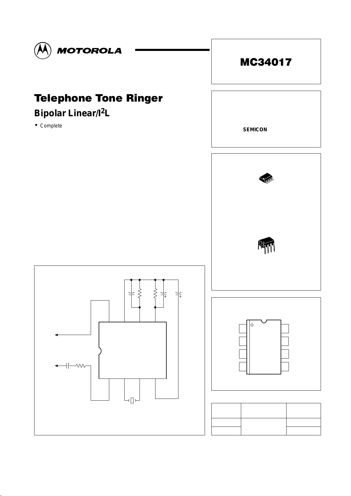
Typical Application
This device contains 97 active transistors and 79 gates.
Piezo Sound
Element
15 k
5.0 µF
25 V
2.2
µ
F
3.0 V
160 k
C
AC2 RG RC RS
AC1 RO1 RO2 RI
8765
1234
Ring
Tip
MC34017–1: C = 1000 pF
MC34017–2: C = 500 pF
MC34017–3: C = 2000 pF
MC34017–X
6.8 k
1.0
µ
F
Motorola, Inc. 1996
Page 2
MC34017
2
MOTOROLA ANALOG IC DEVICE DATA
MAXIMUM RATINGS
(Voltages Referenced to RG, Pin 7)
Rating Symbol Value Unit
Operating AC Input Current (Pins 1, 8) – 20 mA, RMS
Transient Input Current (Pins 1, 8) (T<2.0 ms) V
in
±300 mA, peak
Voltage Applied at RC (Pin 6) V
RC
5.0 V
Voltage Applied at RS (Pin 5) V
RS
5.0 V
Voltage Applied to Outputs (Pins 2, 3) V
O
–2.0 to V
RI
V
Power Dissipation (@ 25°C) P
D
1.0 W
Operating Ambient Temperature T
A
–20 to +60 °C
Storage Temperature T
stg
–65 to +150 °C
NOTE: ESD data available upon request.
ELECTRICAL CHARACTERISTICS (T
A
= 25°C)
Characteristic
Test Symbol Min Typ Max Unit
Ringing Start Voltage Vdc
V
Start
= VI at Ring Start
VI > 0 1a V
Start
(+) 34 37.5 41
VI < 0 1b V
Start
(–) –34 –37.5 –41
Ringing Stop Voltage 1c V
Stop
Vdc
V
Stop
= VI at Ring Stop
MC34017–1 14 16 22
MC34017–2 12 14 20
MC34017–3 14 16 22
Output Frequencies (VI = 50 V) 1d Hz
MC34017–1 High Tone f
H
937 1010 1083
MC34017–1 Low Tone f
L
752 808 868
MC34017–1 Warble Tone f
W
11.5 12.5 14
MC34017–2 High Tone f
H
1874 2020 2166
MC34017–1 Low Tone f
L
1504 1616 1736
MC34017–1 Warble Tone f
W
11.5 12.5 14
MC34017–3 High Tone f
H
937 1010 1083
MC34017–1 Low Tone f
L
752 808 868
MC34017–1 Warble Tone f
W
23 25 28
Output Voltage (VI = 50 V) 6 V
O
34 37 43 Vpp
Output Short–Circuit Current 2 I
RO1
, I
RO2
35 60 80 mApp
Input Diode Voltage (II = 5.0 mA) 3 V
D
5.4 6.2 6.8 Vdc
Input Voltage – SCR “Of f” (II = 30 mA) 4a V
off
30 38 43 Vdc
Input Voltage – SCR “On” (II = 100 mA) 4b V
on
3.2 4.1 6.0 Vdc
RS Clamp Voltage (VI = 50 V) 5 V
clamp
1.3 1.5 1.8 Vdc
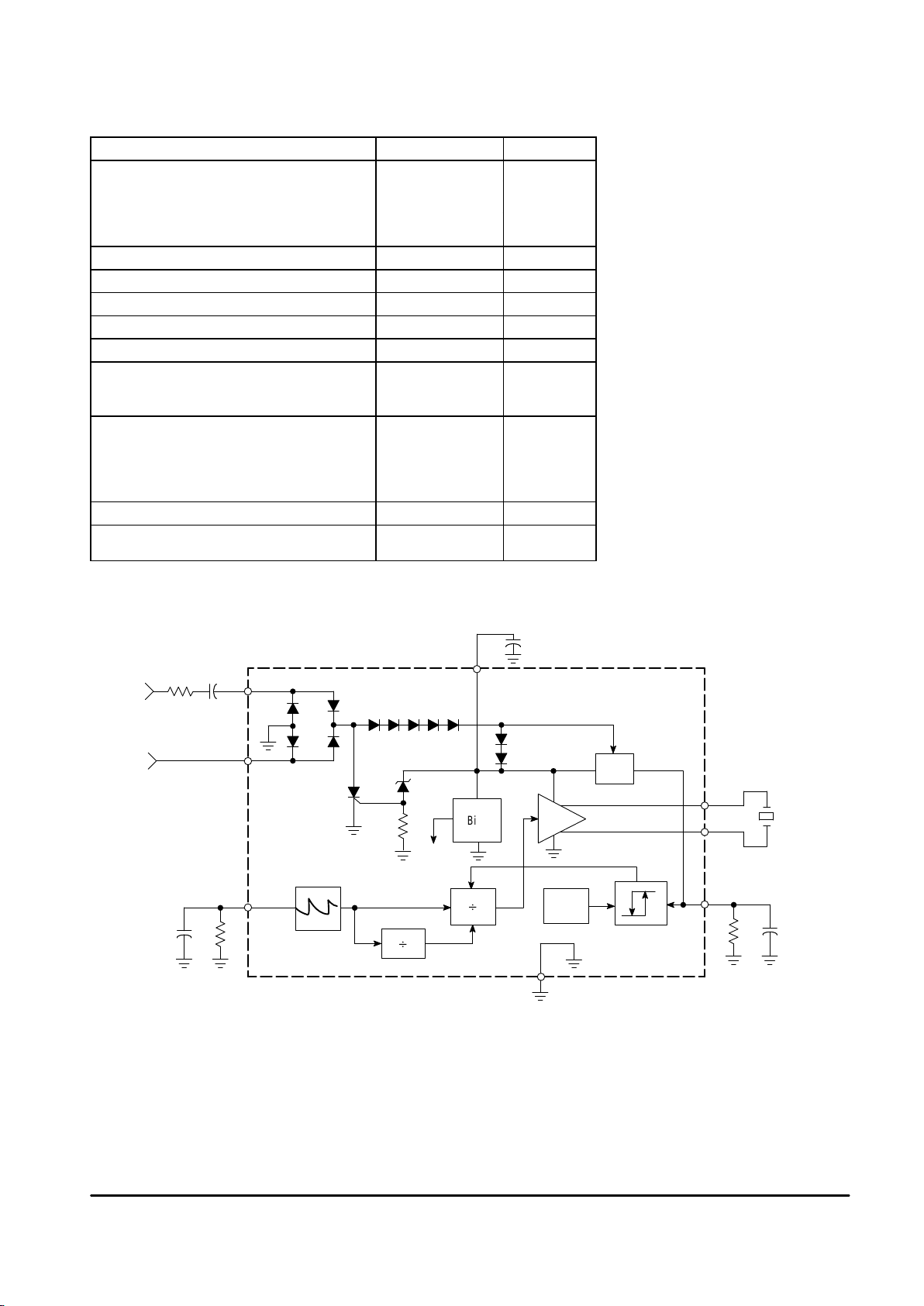
PIN FUNCTION DESCRIPTION
Pin Symbol Description
1, 8 AC1, AC2 The input terminals to the full–wave diode bridge. The ac ringing signal from the telephone line energizes the
ringer through this bridge.
5 RS The input of the threshold comparator to which diode bridge current is mirrored and sensed through an external
resistor (R3). Nominal threshold is 1.2 V . This pin internally clamps at 1.5 V.
4 RI The positive supply terminal for the oscillator, frequency divider and output buffer circuits.
2, 3 RO1, RO2 The tone ringer output terminals through which the sound element is driven.
7 RG The negative terminal of the diode bridge and the negative supply terminal of the tone generating circuitry.
6 RC The oscillator terminal for the external resistor and capacitor which control the tone ringer frequencies (R2, C2).
Page 3
MC34017
3
MOTOROLA ANALOG IC DEVICE DATA
APPLICATION CIRCUIT PERFORMANCE (Refer to Typical Application)
Characteristic Typical Value Units
Output Tone Frequencies Hz
MC34017–1 808/1010
MC34017–2 1616/2020
MC34017–3 404/505
Warble Frequencies 12.5
Output Voltage (VI ≥ 60 Vrms, 20 Hz) 37 Vpp
Output Duty Cycle 50 %
Ringing Start Input Voltage (20 Hz) 36 Vrms
Ringing Stop Input Voltage (20 Hz) 21 Vrms
Maximum AC Input Voltage (≤ 68 Hz) 150 Vrms
Impedance When Ringing kΩ
VI = 40 Vrms, 15 Hz >16
VI = 130 Vrms, 23 Hz 12
Impedance When Not Ringing
VI = 10 Vrms, 24 Hz 28 kΩ
VI = 2.5 Vrms, 24 Hz >1.0 MΩ
VI = 10 Vrms, 5.0 Hz 55 kΩ
VI = 3.0 Vrms, 200 – 3200 Hz >200 kΩ
Maximum Transient Input V oltage (T ≤ 2.0 ms) 1500 V
Ringer Equivalence: Class A 0.5 –
Ringer Equivalence: Class B 0.9 –
8
C1
R1
B
B
Bias
Ref
1
6
RO1
RO2
RS
2
3
5
AC2
AC1
RC
4RI
R2C2
C3R3
22 V
Input
Current
Mirror
Push Pull
Output Buffer
C4
Threshold
Comparator
Oscillator
Tone Frequency
Divider
Warble Frequency
Divider
SCR Transient
Clamp
Diode Bridge
Ring
Piezo
Sound
Element
Tip
Block Diagram
7RG
Page 4

MC34017
4
MOTOROLA ANALOG IC DEVICE DATA
CIRCUIT DESCRIPTION
The MC34017 Tone Ringer derives its power supply by
rectifying the ac ringing signal. It uses this power to activate
a tone generator and drive a piezo–ceramic transducer. The
tone generation circuitry includes a relaxation oscillator and
frequency dividers which produce high and low frequency
tones as well as the tone warble frequency. The relaxation
oscillator frequency fo is set by resistor R2 and capacitor C2
connected to Pin RC. The oscillator will operate with fo from
1.0 kHz to 10 kHz with the proper choice of external
components (see Figure 1).
The frequency of the tone ringer output signal at RO1 and
RO2 alternates between fo/4 to fo/5. The warble rate at which
the frequency changes is fo/320 for the MC34017–1, fo/640
for the MC34017–2 and fo/160 for the MC34017–3. With a
4.0 kHz oscillator frequency, the MC34017–1 produces
800 Hz and 1000 Hz tones with a 12.5 Hz warble rate. The
MC34017–2 generates 1600 Hz and 2000 Hz tones with a
similar 12.5 Hz warble frequency from an 8.0 kHz oscillator
frequency. The MC34017–3 will produce 400 Hz and 500 Hz
tones with a 12.5 Hz warble rate from a 2.0 kHz oscillator
frequency. The tone ringer output circuit can source or sink
20 mA with an output voltage swing of 37 V peak–to–peak.
Volume control is readily implemented by adding a variable
resistance in series with the piezo transducer.
Input signal detection circuitry activates the tone ringer
output when the ac line voltage exceeds programmed
threshold level. Resistor R3 determines the ringing signal
amplitude at which an output signal at RO1 and RO2 will be
generated. The ac ringing signal is rectified by the internal
diode bridge. The rectified input signal produces a voltage
across R3 which is referenced to RG. The voltage across
resistor R3 is filtered by capacitor C3 at the input to the
threshold circuit.
Figure 1. Oscillator Period (1/fo) versus
Oscillator R2 C2 Product
0
800
1/f
o
, OSCILLATOR PERIOD ( s)
µ
R2 C2, OSCILLAT OR R2 C2 PRODUCT (µs)
600
400
200
0
100 200 300 400 500
(1/fo = 1.45 R2 C2 + 10 µs)
150 k ≤ R2 ≤ 300 k
400 pF
≤
C2 ≤ 3000 pF
When the voltage on capacitor C3 exceeds 1.2 V, the
threshold comparator enables the tone ringer output. Line
transients produced by pulse dialing telephones do not charge
capacitor C3 sufficiently to activate the tone ringer output.
Capacitors C1 and C4 and resistor R1 determine the 10 V,
24 Hz signature test impedance. C4 also provides filtering for
the output stage power supply to prevent droop in the square
wave output signal. Six diodes in series with the rectifying
bridge provide the necessary non–linearity for the 2.5 V,
24 Hz signature tests.
An internal shunt voltage regulator between the RI and RG
terminals provides dc voltage to power the output stage,
oscillator and frequency dividers. The dc voltage at RI is
limited to approximately 22 V in regulation. To protect the IC
from telephone line transients, an SCR is triggered when the
regulator current exceeds 50 mA. The SCR diverts current
from the shunt regulator and reduces the power dissipation
within the IC.
EXTERNAL COMPONENTS
R1 Line Input Resistor
R1 affects the tone ringer input impedance. It
also influences ringing threshold voltage and
limits current from line transients.
(Range: 2.0 to 10 kΩ).
C1 Line Input Capacitor
C1 ac couples the tone ringer to the telephone
line and controls ringer input impedance at low
frequencies.
(Range: 0.4 to 2.0 µF).
R2 Oscillator Resistor
(Range: 150 to 300 kΩ).
C2 Oscillator Capacitor
(Range: 400 to 3000 pF).
R3 Input Current Sense Resistor
R3 controls the ringing threshold voltage.
Increasing R3 decreases the ring–start voltage.
(Range: 5.0 to 18 kΩ).
C3 Ringing Threshold Filter Capacitor
C3 filters the ac voltage across R3 at the input
of the ringing threshold comparator. It also
provides dialer transient rejection.
(Range: 0.5 to 5.0 µF).
C4 Ringer Supply Capacitor
C4 filters supply voltage for the tone generating
circuits. It also provides an ac current path for
the 10 Vrms ringer signature impedance.
(Range: 1.0 to 10 µF).
Page 5

MC34017
5
MOTOROLA ANALOG IC DEVICE DATA
S1
(Normally Open)
Figure 2. Test One
1
2
3
8
7
6
5
AC1
RO1
RO2
RI
4
AC2
RG
RC
RS
1
2
3
4
16
15
14
13
5
6
7
8
12
11
10
9
160 k*
C
15 k*
0.2
µ
F
1.0 µF
0.01
µ
F*
6.8 k*
V
I
V
O
390
Ω
0.047 µF
V
DD
V
DD
IC2
DUT
5.6 k
10 k
V
DD
0.01
µ
F
Q1
0.1
µ
F
R
12
13
9
8
11
10
200 k
f
H
f
L
f
W
IC1 – MC14011B
IC2 – MC14538B
Q1 – 2N3904
MC34017–1: R = 110 k
Ω
*
MC34017–2: R = 55 k
Ω
*
MC34017–3: R = 110 k
Ω
*
MC34017–1: C = 1000 pF*
MC34017–2: C = 500 pF*
MC34017–3: C = 1000 pF*
a. Increase VI from +33 V while monitoring VO.
V
Start
(+) equals VI when VO commences switching.
b. Decrease VI from –33 V while monitoring VO.
V
Start
(–) equals VI when VO commences switching.
c. Decrease VI from +40 V while monitoring VO.
V
Stop
equals VI when VO ceases switching.
d. Set VI to +50 V. Close S1. Measure frequencies
fH, fL and fW.
*Indicates 1% tolerance (5% otherwise)
VDD = 12 V
10 k
1/4
IC1
1/4
IC1
Page 6

MC34017
6
MOTOROLA ANALOG IC DEVICE DATA
Figure 3. Test Two
1
2
3
8
7
6
5
AC1
RO1
RO2
RI
4
AC2
RG
RC
RS
160 k*
C
15 k*
0.2
µ
F
6.8 k*
DUT
*Indicates 1% tolerance (5% otherwise)
MC34017–1: C = 1000 pF*
MC34017–2: C = 500 pF*
MC34017–3: C = 1000 pF*
With VRC = 4.0 V, close S1. Switch S2 to Pin 2 and measure current
at Pin 2 (IO1). Repeatedly switch VRC between 4.0 V and 0 V until
Pin 2 current changes polarity. Measure the opposite polarity current (IO2).
S1
2.0 k
10 V
5.0 V
I
RO1
I
RO2
S2
50 V
V
RC
Calculate: I
RO2
= |IO1| + |IO2|.
Calculate: I
RO1
= |IO1| + |IO2|.
Switch S2 to Pin 3 and repeat.
Figure 4. Test Three
1
2
3
8
7
6
5
AC1
RO1
RO2
R1
4
AC2
RG
RC
RS
160 k*
C
15 k*
0.2
µ
F
V
D
390
Ω
0.047 µF
DUT
*Indicates 1% tolerance (5% otherwise)
Measure voltage at Pin 1.
MC34017–1: C = 1000 pF*
MC34017–2: C = 500 pF*
MC34017–3: C = 1000 pF*
5.0
mA
Page 7

MC34017
7
MOTOROLA ANALOG IC DEVICE DATA
Figure 5. Test Four
1
2
3
8
7
6
5
AC1
RO1
RO2
RI
4
AC2
RG
RC
RS
160 k*
C
15 k*
0.2
µ
F
V
DUT
*Indicates 1% tolerance (5% otherwise)
(Each test < 30 ms)
MC34017–1: C = 1000 pF*
MC34017–2: C = 500 pF*
MC34017–3: C = 1000 pF*
a. Set I1 to 30 mA. Measure voltage at Pin 1 (V
off
).
I1
b. Set I1 to 100 mA. Measure voltage at Pin 1 (Von).
Figure 6. Test Five
1
2
3
8
7
6
5
AC1
RO1
RO2
RI
4
AC2
RG
RC
RS
160 k*
C
15 k*
DUT
*Indicates 1% tolerance (5% otherwise)
MC34017–1: C = 1000 pF*
MC34017–2: C = 500 pF*
MC34017–3: C = 1000 pF*
50 V
V
clamp
6.8 k*
Measure voltage at Pin 5 (V
clamp
).
Figure 7. Test Six
1
2
3
8
7
6
5
AC1
RO1
RO2
RI
4
AC2
RG
RC
RS
160 k*
C
15 k*
0.2
µ
F
6.8 k*
DUT
*Indicates 1% tolerance (5% otherwise)
MC34017–1: C = 1000 pF*
MC34017–2: C = 500 pF*
MC34017–3: C = 1000 pF*
S1
2.0 k
50 V
V
RC
20 k
V
O
With VRC = 4.0 V, close S1. Measure dc voltage between Pins 2 and 3
(VO1). Repeatedly switch VRC between 4.0 V and 0 V until Pins 2 and 3
change state. Measure the new voltage between Pins 2 and 3 (VO2).
Calculate: VO = |VO1| + |VO2|.
Page 8

MC34017
8
MOTOROLA ANALOG IC DEVICE DATA
D SUFFIX
PLASTIC PACKAGE
CASE 751–05
ISSUE N
P SUFFIX
PLASTIC PACKAGE
CASE 626–05
ISSUE K
OUTLINE DIMENSIONS
NOTES:
1. DIMENSIONING AND TOLERANCING PER
ANSI Y14.5M, 1982.
2. CONTROLLING DIMENSION: MILLIMETER.
3. DIMENSIONS A AND B DO NOT INCLUDE
MOLD PROTRUSION.
4. MAXIMUM MOLD PROTRUSION 0.15 (0.006)
PER SIDE.
5. DIMENSION D DOES NOT INCLUDE DAMBAR
PROTRUSION. ALLOWABLE DAMBAR
PROTRUSION SHALL BE 0.127 (0.005) TOTAL
IN EXCESS OF THE D DIMENSION AT
MAXIMUM MATERIAL CONDITION.
SEATING
PLANE
14
58
C
K
4X P
A0.25 (0.010)MTB
SS
0.25 (0.010)MB
M
8X D
R
M
J
X 45
_
_
F
–A–
–B–
–T–
DIM MIN MAX MIN MAX
INCHESMILLIMETERS
A 4.80 5.00 0.189 0.196
B 3.80 4.00 0.150 0.157
C 1.35 1.75 0.054 0.068
D 0.35 0.49 0.014 0.019
F 0.40 1.25 0.016 0.049
G 1.27 BSC 0.050 BSC
J 0.18 0.25 0.007 0.009
K 0.10 0.25 0.004 0.009
M 0 7 0 7
P 5.80 6.20 0.229 0.244
R 0.25 0.50 0.010 0.019
____
G
NOTES:
1. DIMENSION L TO CENTER OF LEAD WHEN
FORMED PARALLEL.
2. PACKAGE CONTOUR OPTIONAL (ROUND OR
SQUARE CORNERS).
3. DIMENSIONING AND TOLERANCING PER ANSI
Y14.5M, 1982.
14
58
F
NOTE 2
–A–
–B–
–T–
SEATING
PLANE
H
J
G
D
K
N
C
L
M
M
A
M
0.13 (0.005) B
M
T
DIM MIN MAX MIN MAX
INCHESMILLIMETERS
A 9.40 10.16 0.370 0.400
B 6.10 6.60 0.240 0.260
C 3.94 4.45 0.155 0.175
D 0.38 0.51 0.015 0.020
F 1.02 1.78 0.040 0.070
G 2.54 BSC 0.100 BSC
H 0.76 1.27 0.030 0.050
J 0.20 0.30 0.008 0.012
K 2.92 3.43 0.115 0.135
L 7.62 BSC 0.300 BSC
M ––– 10 ––– 10
N 0.76 1.01 0.030 0.040
__
Motorola reserves the right to make changes without further notice to any products herein. Motorola makes no warranty , representation or guarantee regarding
the suitability of its products for any particular purpose, nor does Motorola assume any liability arising out of the application or use of any product or circuit, and
specifically disclaims any and all liability, including without limitation consequential or incidental damages. “T ypical” parameters which may be provided in Motorola
data sheets and/or specifications can and do vary in different applications and actual performance may vary over time. All operating parameters, including “Typicals”
must be validated for each customer application by customer’s technical experts. Motorola does not convey any license under its patent rights nor the rights of
others. Motorola products are not designed, intended, or authorized for use as components in systems intended for surgical implant into the body, or other
applications intended to support or sustain life, or for any other application in which the failure of the Motorola product could create a situation where personal injury
or death may occur. Should Buyer purchase or use Motorola products for any such unintended or unauthorized application, Buyer shall indemnify and hold Motorola
and its officers, employees, subsidiaries, affiliates, and distributors harmless against all claims, costs, damages, and expenses, and reasonable attorney fees
arising out of, directly or indirectly, any claim of personal injury or death associated with such unintended or unauthorized use, even if such claim alleges that
Motorola was negligent regarding the design or manufacture of the part. Motorola and are registered trademarks of Motorola, Inc. Motorola, Inc. is an Equal
Opportunity/Affirmative Action Employer.
How to reach us:
USA/EUROPE/Locations Not Listed: Motorola Literature Distribution; JAPAN: Nippon Motorola Ltd.; Tatsumi–SPD–JLDC, 6F Seibu–Butsuryu–Center,
P.O. Box 20912; Phoenix, Arizona 85036. 1–800–441–2447 or 602–303–5454 3–14–2 Ta tsumi Koto–Ku, Tokyo 135, Japan. 03–81–3521–8315
MFAX: RMF AX0@email.sps.mot.com – TOUCHT ONE 602–244–6609 ASIA/PACIFIC: Motorola Semiconductors H.K. Ltd.; 8B Tai Ping Industrial Park,
INTERNET: http://Design–NET.com 51 Ting Ko k Road, Tai Po, N.T., Hong Kong. 852–26629298
MC34017/D
*MC34017/D*
◊
 Loading...