

Page 1
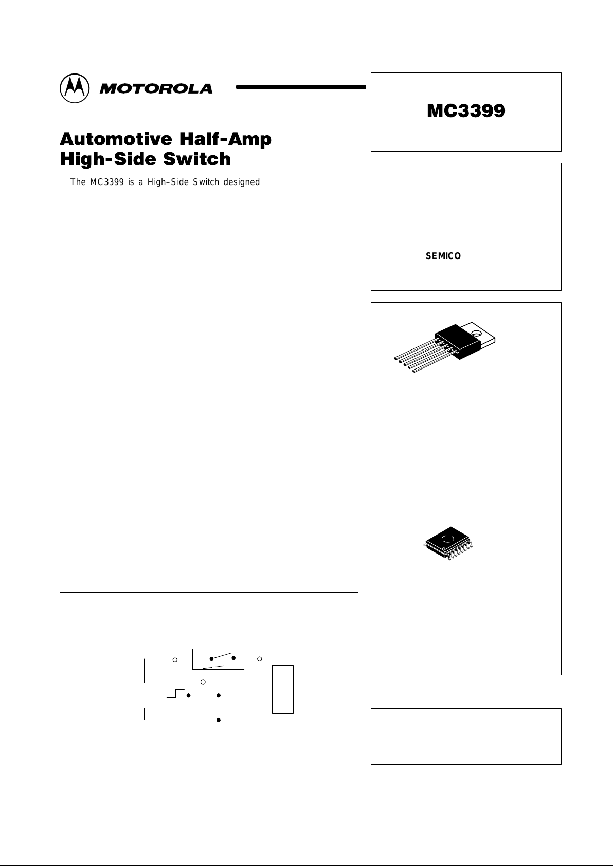
Device
Operating
Temperature Range
Package
SEMICONDUCTOR
TECHNICAL DATA
AUTOMOTIVE
HALF–AMP HIGH–SIDE
SWITCH
ORDERING INFORMATION
MC3399DW
MC3399T
TA = – 40° to +125°C
SOP(8+8)L
Plastic Power
DW SUFFIX
PLASTIC PACKAGE
CASE 751G
SOP(8+8)L
16
1
Order this document by MC3399/D
Pin 1. Ignition
2. N.C.
3. N.C.
4. N.C.
5. Ground
6. N.C.
7. Input
8. N.C.
9. Output
10.Output
11.Output
12.Output
13.Output
14.Output
15.Output
16.Output
T SUFFIX
PLASTIC PACKAGE
CASE 314D
1
5
Pin 1. Ignition
2. Output
3. Output
4. Ground
5. Input
Pins 2 and 3 connected to package tab.
1
MOTOROLA ANALOG IC DEVICE DATA
The MC3399 is a High–Side Switch designed to drive loads from the
positive side of the power supply. The output is controlled by a TTL
compatible input Enable pin. In the “on” state, the device exhibits very low
saturation voltages for load currents in excess of 750 mA. The device
isolates the load from positive or negative going high voltage transients by
abruptly “opening” thus protecting the load from the transient voltage for the
duration of the transient. The device automatically re–establishes its original
operating state following the transient condition.
The MC3399 is fabricated on a power BIMOS process which combines
the best features of Bipolar and MOS technologies. The mixed technology
provides higher gain PNP output devices and results in Power Integrated
Circuits having substantially reduced quiescent currents.
The device operates over a wide power supply voltage range and can
withstand voltage transients (positive or negative) of ±100 V. A rugged PNP
output stage along with active clamp circuitry, output current limit and
thermal shutdown permit the driving of all types of loads, including inductive.
The MC3399 is offered in 5–lead TO–220 and 16–lead SOIC plastic
packages to facilitate either “thru–hole” or surface mount use. In addition, it
is specified over a wide ambient operating temperature of –40°C to +125°C
and is ideally suited for industrial and automotive applications where harsh
environments exist.
• Low Switch Voltage Drop
• Load Currents in Excess of 750 mA
• Low Quiescent Current
• Transient Protection Up to ±100 V
• TTL Compatible Enable Input
• On–Chip Current Limit and Thermal Shutdown Circuitry
Representative Block Diagram
Ignition Output
Input
Gnd
L
O
A
D
Power
Supply
MC3399T
This device contains 52 active transistors.
Motorola, Inc. 1997 Rev 1
Page 2
MC3399
2
MOTOROLA ANALOG IC DEVICE DATA
MAXIMUM RATINGS
Rating Symbol Value Unit
Ignition Input Voltage (Continuous) V
IGN
Vdc
Forward 25
Reverse –16
Ignition Input Voltage (T ransient) V
IGN
V
±60
±100
Input Voltage V
in
–0.3 to +7.0 V
Output Current I
O
Internally
Limited
A
Thermal Resistance °C/W
Plastic Power Package (Case 314D)
Junction–to–Ambient R
θJA1
65
Junction–to–Tab R
θJT
5.0
SOP(8+8)L Plastic Package (Case 751G)
Junction–to–Ambient R
θJA2
138
Junction–to–Lead 12 R
θJL
52
Soldering Temperature (for 10 Seconds) T
solder
260 °C
Junction Temperature T
J
–40 to +150 °C
Storage Temperature T
stg
–65 to +150 °C
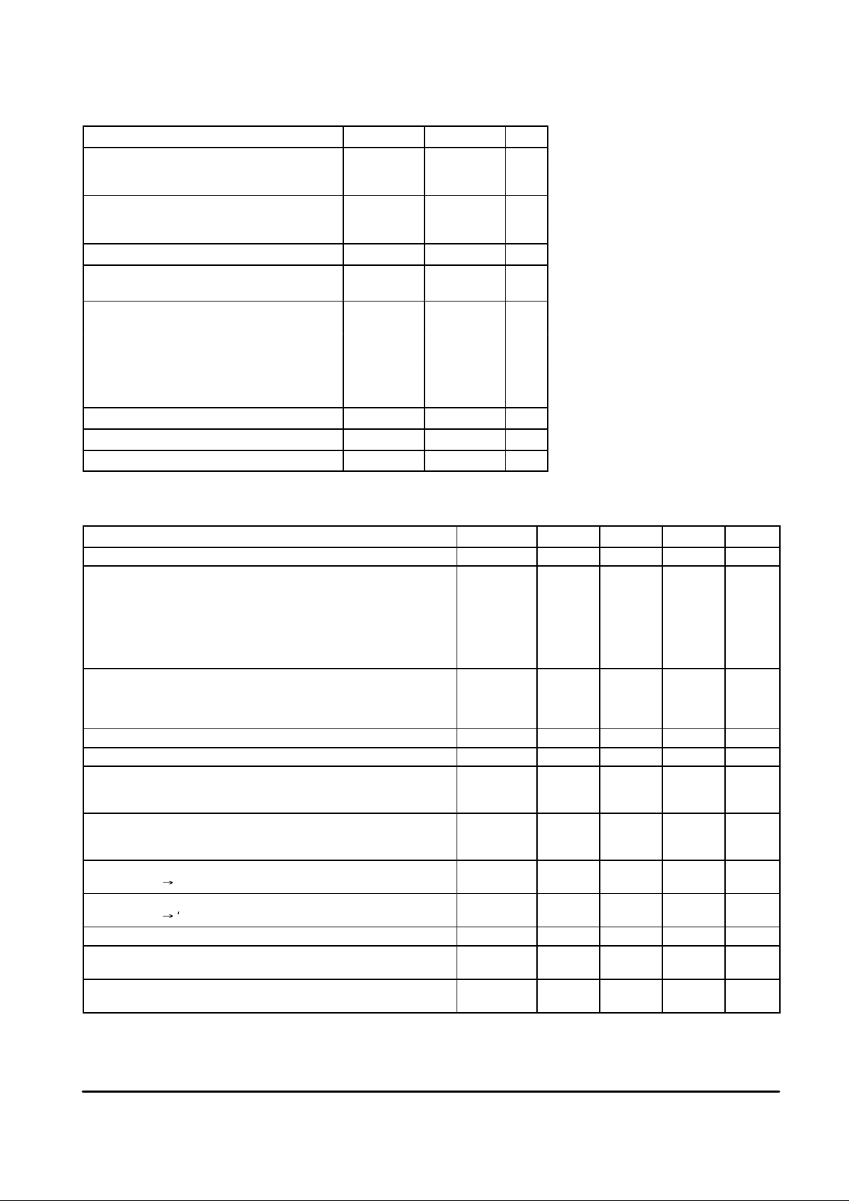
ELECTRICAL CHARACTERISTICS (V
IGN
= 12 V, IL = 150 mA, –40°C ≤ TA = +125°C, V Input = “1”, unless otherwise noted.)
(1)
Characteristic
Symbol Min Typ Max Unit
Operating Voltage V
IGN(min)
4.5 – – V
Switch Voltage Drop (Saturation)
V
IGN
= 4.5 V IO = 150 mA, TA = 25°C
IO = 200 mA, TA = –40°C
IO = 125 mA, TA = 125°C
V
IGN
= 12 V IO = 425 mA, TA = 25°C
IO = 550 mA, TA = –40°C
V
IGN
= 16 V IO = 375 mA, TA = 125°C
V
IGN–VO
–
–
–
–
–
–
0.2
0.3
0.3
0.3
0.3
0.4
0.5
0.5
0.5
0.7
0.7
0.7
V
Quiescent Current
V
IGN
= 12 V IO = 150 mA, TA = 25°C
IO = 550 mA, TA = –40°C
IO = 300 mA, TA = 125°C
I
GND
–
–
–
12
25
10
50
100
50
mA
Output Current Limit (VO = 0 V) I
SC
– 1.6 2.5 A
Output Leakage Current (V
IGN
= 12 V , Input = “0”) I
Leak
– 10 150 µA
Input Voltage
High Logic State
Low Logic State
V
IH
V
IL
2.0
–
–
–
–
0.8
V
Input Current
High Logic State (VIH = 5.5 V)
Low Logic State (VIL = 0.4 V)
I
IH
I
IL
–
–
120
20
–
–
µA
Output Turn–On Delay Time
Input = ‘‘0’’ ³ ‘‘1’’, TA = +25°C (Figures 1 and 3)
t
DLY(on)
– 50 – µs
Output Turn–Off Delay Time
Input = ‘‘1’’ ³ ‘‘0’’, TA = +25°C (Figures 1 and 3)
t
DLY(off)
– 5.0 – µs
Overvoltage Shutdown Threshold V
in(OV)
26 31 36 V
Output Turn–Off Delay Time (TA = + 25°C) to Overvoltage Condition,
Vin stepped from 12 V to 40 V , V ≤ 0.9 VO (Figures 1 and 3)
t
DLY
– 2.0 – µs
Output Recovery Delay Time (TA = + 25°C)
V
IGN
stepped from 40 V to 12 V , V ≥ 0.9 VO (Figures 1 and 3)
t
RCVY
– 5.0 – µs
NOTES: 1. Typical values represent characteristics of operation at TA = 25°C.
Page 3

MC3399
3
MOTOROLA ANALOG IC DEVICE DATA
NOTE: * Depending on load current and transient duration, an output capacitor
(CO) of sufficient value may be used to hold up output voltage during the
transient, and absorb turn–off delay voltage overshoot.
Transient
Generator
+
12 V
Input
Thermal
Sense
Control
Circuit
Current
Limit
35 V
35 V
I
L
R
L
50
Ω
Ground
Ignition Output*
–
40 V
Ignition
12 V
Input
5.0 V
0 V
31 V
Output
V
O
12 V
0 V
0.9 V
O
t
DLY(OV)
t
RCVY
t
DLT(off)tDLY(on)
0.9 V
O
0
200
400
600
800
0 200 400 600 800 1000
0
20
40
60
80
0 200 400 600 800 1000
IL, LOAD CURRENT (mA) IL, LOAD CURRENT (mA)
VOLTAGE DIFFERENTIAL (mV)
I , QUIESCENT CURRENT (mA)
Q
V
IGN
= 24 V
TA = 25
°
C
Vin = “1”
V
IGN
= 24 V
TA = 25
°
C
Vin = “1”
V –V , IGNITION TO OUTPUT
OIGN
Line Transient
1.0 ms
Ignition
1.0 ms
100 V
31 V
12 V
0 V
–100 V
5.0 V
0 V
31 V
12 V
0 V
Input
Output
(Load Voltage)
Figure 1. Transient Response Test Circuit
Figure 2. Timing Diagram Figure 3. Response Time Diagram
Figure 4. Switch Voltage Drop
versus Load Current
Figure 5. Quiescent Current
versus Load Current
Page 4

MC3399
4
MOTOROLA ANALOG IC DEVICE DATA
T SUFFIX
PLASTIC PACKAGE
CASE 314D–03
ISSUE D
DW SUFFIX
PLASTIC PACKAGE
CASE 751G–03
(SOP(8+8)L)
ISSUE B
OUTLINE DIMENSIONS
–Q–
12345
U
K
D
G
S
A
B
5 PL
J
H
L
E
C
M
Q
M
0.356 (0.014) T
SEATING
PLANE
–T–
DIM MIN MAX MIN MAX
MILLIMETERSINCHES
A 0.572 0.613 14.529 15.570
B 0.390 0.415 9.906 10.541
C 0.170 0.180 4.318 4.572
D 0.025 0.038 0.635 0.965
E 0.048 0.055 1.219 1.397
G 0.067 BSC 1.702 BSC
H 0.087 0.112 2.210 2.845
J 0.015 0.025 0.381 0.635
K 1.020 1.065 25.908 27.051
L 0.320 0.365 8.128 9.271
Q 0.140 0.153 3.556 3.886
U 0.105 0.117 2.667 2.972
S 0.543 0.582 13.792 14.783
NOTES:
1. DIMENSIONING AND TOLERANCING PER ANSI
Y14.5M, 1982.
2. CONTROLLING DIMENSION: INCH.
3. DIMENSION D DOES NOT INCLUDE
INTERCONNECT BAR (DAMBAR) PROTRUSION.
DIMENSION D INCLUDING PROTRUSION SHALL
NOT EXCEED 10.92 (0.043) MAXIMUM.
D
14X
B16X
SEATING
PLANE
S
A
M
0.25 B
S
T
16 9
81
h X 45
_
M
B
M
0.25
H8X
E
B
A
e
T
A1
A
L
C
q
NOTES:
1. DIMENSIONS ARE IN MILLIMETERS.
2. INTERPRET DIMENSIONS AND TOLERANCES
PER ASME Y14.5M, 1994.
3. DIMENSIONS D AND E DO NOT INLCUDE MOLD
PROTRUSION.
4. MAXIMUM MOLD PROTRUSION 0.15 PER SIDE.
5. DIMENSION B DOES NOT INCLUDE DAMBAR
PROTRUSION. ALLOWABLE DAMBAR
PROTRUSION SHALL BE 0.13 TOTAL IN EXCESS
OF THE B DIMENSION AT MAXIMUM MATERIAL
CONDITION.
DIM MIN MAX
MILLIMETERS
A 2.35 2.65
A1 0.10 0.25
B 0.35 0.49
C 0.23 0.32
D 10.15 10.45
E 7.40 7.60
e 1.27 BSC
H 10.05 10.55
h 0.25 0.75
L 0.50 0.90
q
0 7
__
Page 5

MC3399
5
MOTOROLA ANALOG IC DEVICE DATA
Motorola reserves the right to make changes without further notice to any products herein. Motorola makes no warranty , representation or guarantee regarding
the suitability of its products for any particular purpose, nor does Motorola assume any liability arising out of the application or use of any product or circuit, and
specifically disclaims any and all liability, including without limitation consequential or incidental damages. “T ypical” parameters which may be provided in Motorola
data sheets and/or specifications can and do vary in different applications and actual performance may vary over time. All operating parameters, including “Typicals”
must be validated for each customer application by customer’s technical experts. Motorola does not convey any license under its patent rights nor the rights of
others. Motorola products are not designed, intended, or authorized for use as components in systems intended for surgical implant into the body, or other
applications intended to support or sustain life, or for any other application in which the failure of the Motorola product could create a situation where personal injury
or death may occur. Should Buyer purchase or use Motorola products for any such unintended or unauthorized application, Buyer shall indemnify and hold Motorola
and its officers, employees, subsidiaries, affiliates, and distributors harmless against all claims, costs, damages, and expenses, and reasonable attorney fees
arising out of, directly or indirectly, any claim of personal injury or death associated with such unintended or unauthorized use, even if such claim alleges that
Motorola was negligent regarding the design or manufacture of the part. Motorola and are registered trademarks of Motorola, Inc. Motorola, Inc. is an Equal
Opportunity/Affirmative Action Employer.
Page 6

MC3399
6
MOTOROLA ANALOG IC DEVICE DATA
Mfax is a trademark of Motorola, Inc.
How to reach us:
USA/EUROPE/ Locations Not Listed: Motorola Literature Distribution; JAP AN: Nippon Motorola Ltd.: SPD, Strategic Planning Office, 141,
P.O. Box 5405, Denver, Colorado 80217. 1–303–675–2140 or 1–800–441–2447 4–32–1 Nishi–Gotanda, Shagawa–ku, Tokyo, Japan. 03–5487–8488
Customer Focus Center: 1–800–521–6274
Mfax: RMFAX0@email.sps.mot.com – TOUCHTONE 1–602–244–6609 ASIA/PACIFIC: Motorola Semiconductors H.K. Ltd.; 8B Tai Ping Industrial Park,
Moto rola Fax Back Sys tem – US & Canada ONLY 1–800–774–1848 51 Ting Kok Road, Tai Po, N.T., Hong Kong. 852–26629298
– http://sps.motorola.com/mfax/
HOME PAGE: http://motorola.com/sps/
MC3399/D
◊
 Loading...