

Page 1
Semiconductor Components Industries, LLC, 2000
April, 2000 – Rev. 2
1 Publication Order Number:
MC33765/D
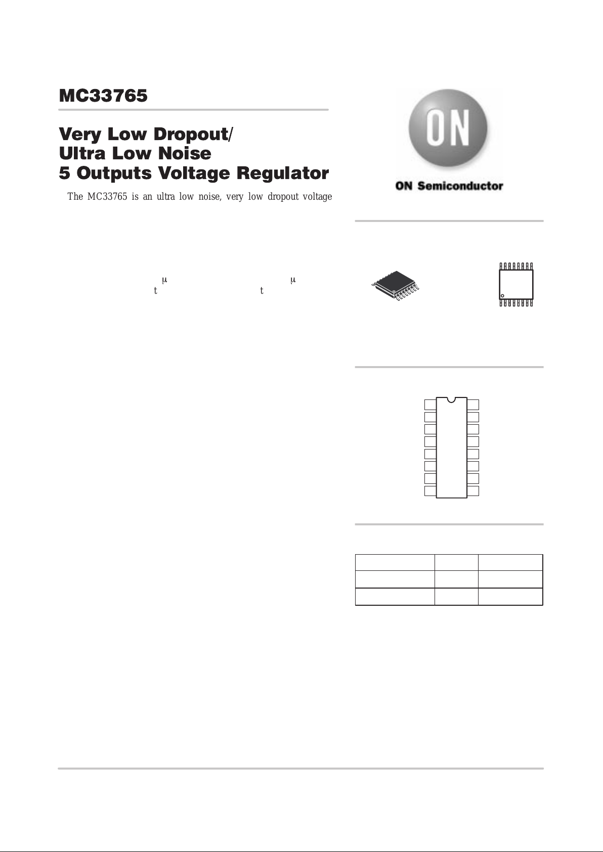
MC33765
V ery Low Dropout/
Ultra Low Noise
5 Outputs V oltage Regulator
The MC33765 is an ultra low noise, very low dropout voltage
regulator with five independent outputs which is available in TSSOP
16 surface mount package.
The MC33765 is available in 2.8 V. The output voltage is the same
for all five outputs but each output is capable of supplying different
currents up to 150 mA for output 4. The device features a very low
dropout voltage (0.11 V typical for maximum output current), very
low quiescent current (5.0 mA maximum in OFF mode, 130 mA typical
in ON mode) and one of the output (output 3) exhibits a very low noise
level which allows the driving of noise sensitive circuitry. Internal
current and thermal limiting protections are provided.
Additionally , the MC33765 has an independent Enable input pin for
each output. It includes also a common Enable pin to shutdown the
complete circuit when not used. The Common Enable pin has the
highest priority over the five independent Enable input pins.
The voltage regulators VR1, VR2 and VR3 have a common input
voltage pin VCC1.
The other voltage regulators VR4 and VR5 have a common input
voltage pin VCC2.
• Five Independent Outputs at 2.8V Typical, based upon voltage
version
• Internal Trimmed Voltage Reference
• V
out
Tolerance ±3.0% over the Temperature Range –40°C to +85°C
• Enable Input Pin (Logic–Controlled Shutdown) for Each of the Five
Outputs
• Common Enable Pin to Shutdown the Whole Circuit
• Very Low Dropout Voltage (0.11 V Typical for Output 1, 2, 3 and 5;
0.17 V Typical for Output 4 at Maximum Current)
• Very Low Quiescent Current (Maximum 5.0 µA in OFF Mode,
130 µA Typical in ON Mode)
• Ultra Low Noise for VR3 (30 µV RMS Max, 100 Hz < f < 100 kHz)
• Internal Current and Thermal Limit
• 100 nF for VR1, VR2, VR4 and VR5 and 1.0 µF for VR3 for
Stability
• Supply Voltage Rejection: 60 dB (Typical) @ f = 1.0 kHz
Device Package Shipping
ORDERING INFORMATION
MC33765DTB TSSOP16 96 Units/Rail
MC33765DTBR2 TSSOP16
TSSOP–16
DTB SUFFIX
CASE 948F
1
16
http://onsemi.com
2500 Units/Reel
MARKING
DIAGRAMS
PIN CONNECTIONS
116
15
14
13
12
11
10
9
2
3
4
5
6
7
8
(Top View)
Bypass
Common Enable
On/Off V–Reg. 1
GND
Not Connected
Output V–Reg. 5
MC33765
On/Off V–Reg. 2
On/Off V–Reg. 3
On/Off V–Reg. 4
On/Off V–Reg. 5 VCC2
Output V–Reg. 4
Output V–Reg. 3
Output V–Reg. 2
Output V–Reg. 1
VCC1
MC33
765
ALYW
1
16
A = Assembly Location
WL, L = Wafer Lot
YY, Y = Year
WW, W= Work Week
Page 2
MC33765
http://onsemi.com
2
Enable
Current
Limit
Temp.
Shut.
Enable
Current
Limit
Temp.
Shut.
Enable
Current
Limit
Temp.
Shut.
Enable
Current
Limit
Temp.
Shut.
Enable
Current
Limit
Temp.
Shut.
Common
Enable
+
–
+
–
+
–
+
–
+
–
Simplified Block Diagram
330 nF
V
OUT
1
VCC2
(14)
100 nF
V
OUT
2
(13)
100 nF
V
OUT
3
(12)
1.0 mF
V
OUT
4
(11)
100 nF
V
OUT
5
(9)
100 nF
VCC1
VCC1
VCC1
VCC2
VCC2
(8)
GND
(7)
ON/OFF 5
(6)
ON/OFF 4
(5)
ON/OFF 3
VCC1
(4)
ON/OFF 2
BYPASS
(3)
ON/OFF 1
Voltage
Reference
1.25 V
(15) (2)CE
100 nF
(10)
Page 3
MC33765
http://onsemi.com
3
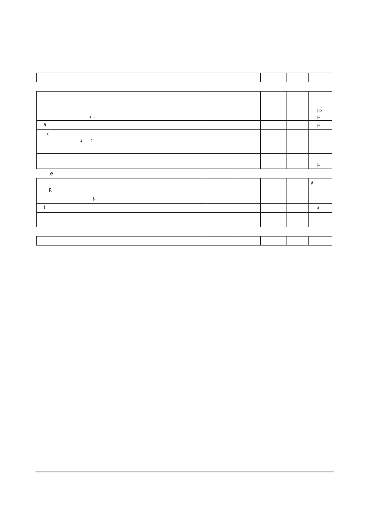
MAXIMUM RATINGS
Rating Symbol Pin # Value Unit
Power Supply Voltage
ÁÁÁÁ
V
CC
5.3
ÁÁÁ
V
Thermal Resistance Junction–to–Air
ÁÁÁÁ
R
q
JA
140
ÁÁÁ
°C/W
Operating Ambient Temperature
ÁÁÁÁ
T
A
–40 to +85
ÁÁÁ
°C
Maximum Operating Junction Temperature
ÁÁÁÁ
T
J
125
ÁÁÁ
°C
Maximum Junction Temperature
ÁÁÁÁ
T
Jmax
150
ÁÁÁ
°C
Storage Temperature Range
ÁÁÁÁ
T
stg
–60 to +150
ÁÁÁ
°C
CONTROL ELECTRICAL CHARACTERISTICS
ELECTRICAL CHARACTERISTICS (For typical values T
A
= 25°C, for min/max values TA = –40°C to +85°C/ Max TJ = 125°C)
Characteristics
Symbol Pin # Min Typ Max Unit
Independent Enable Pins
Input Voltage Range V
ON/OFF(1–5)
0 – V
CC
V
Control Input Impedance
100
–
–
k
W
Logic “0”, i.e. OFF State V
ON/OFF(1–5)
– – 0.5 V
Logic “1”, i.e. ON State 2.0 – –
Common Enable Pin
Input Voltage Range V
CE
2 0 – V
CC
V
Control Input Impedance
2
100
–
–
k
W
Logic “0”, i.e. OFF State V
CE
2 – – 0.3 V
Logic “1”, i.e. ON State 2.0 – –
ELECTRICAL CHARACTERISTICS (For typical values T
A
= 25°C, for min/max values TA = –40°C to +85°C/ Max TJ = 125°C)
Characteristics
Symbol Min Typ Max Unit
CURRENT CONSUMPTION with NO LOAD
Current Consumption at Logic “0” for the complete device,
IQ
OFF
m
A
i.e. Common Enable and All Independent Enable pins at OFF State – – 5.0
Current Consumption at Logic “1” for the complete device,
IQ
ON1
m
A
i.e. Common Enable and All Independents Enable pins at ON State – 470 –
Current Consumption at Logic “1”, Common Enable at ON State
IQ
ON2
m
A
and All Independents Enable pins at OFF State – 130 –
Page 4
MC33765
http://onsemi.com
4
REGULA T OR ELECTRICAL CHARACTERISTICS
ELECTRICAL CHARACTERISTICS (For typical values T
A
= 25°C, for min/max values TA = –40°C to +85°C/ Max TJ = 125°C)
Characteristics Symbol Pin # Min Typ Max Unit
Supply and Output Voltages, Dropout and Load Regulation
Supply Voltage V
CC
MC33765 (2.8V) V
CC1, VCC2
15, 10 3.0 3.6 5.3 V
Regulator Output Voltage for VR1, VR2, VR3, VR4 and VR5 V
OUT(1–5)
14, 13, 12, V
MC33765 (2.8V) 11, 9 2.7 2.8 2.85
Dropout Voltage for VR1, VR2, VR3, VR5 (Note 1.) VCC–V
OUT
14, 13, – 0.11 0.17 V
12, 9
Dropout Voltage for VR4 (Note 1.) VCC–V
OUT4
11 – 0.17 0.30 V
Load Regulation (TA = 25°C) Reg
load(1–5)
9, 11, 12, – – 0.5 mV/
mA
13, 14
Max Power Dissipation and Total DC Output Current (VR1 + VR2 + VR3 + VR4 + VR5) (Note 2.)
Max Power Dissipation at VCC = 5.3 V (TA = 85°C) P
dmax
– – 285 mW
Max. Total RMS Output Current at VCC = 5.3 V (TA = 85°C) I
RMS
– – 130 mA
Max Power Dissipation at VCC = 5.3 V (TA = 25°C) P
dmax
– – 700 mW
Max. Total RMS Output Current at VCC = 5.3 V (TA = 25°C) I
RMS
– – 250 mA
Output Currents (Note 3.)
Regulator VR1 Output Current I
OUT1
14 10 – 30 mA
Regulator VR2 Output Current I
OUT2
13 10 – 40 mA
Regulator VR3 Output Current I
OUT3
12 0 – 50 mA
Regulator VR4 Output Current I
OUT4
11 10 – 150 mA
Regulator VR5 Output Current I
OUT5
9 10 – 60 mA
Current Limit for VR1, VR2, VR3, VR4, VR5 I
MAX
14, 13, 12, – 2 X I
OUT
– mA
[Twice the max Output Current for each output] 11, 9 (1–5)
External Capacitors
External Compensation Capacitors for VR1, VR2, VR4, VR5 C
(1–2, 4–5)
14, 13, 11, 9 0.10 – 1.0
m
F
External Compensation Capacitors for VR3 C
4
12 1.0 – –
m
F
External Compensation Capacitors ESR 0.05 1.0 3.0
W
Ripple Rejections
Ripple Rejection VR1, VR2, VR4, VR5
(DV
OUT
)
14, 13, 50 60 – dB
(at Max. Current, 1.0 kHz, C = 100 nF)
(DVCC)
11, 9
Ripple Rejection VR1, VR2, VR4, VR5
(DV
OUT
)
14, 13, 40 45 – dB
(at Max. Current, f = 10 kHz, C = 100 nF)
(DVCC)
11, 9
Ripple Rejection of VR3
(DV
OUT
)
12 50 60 – dB
(at Max. Current, f = 1.0 kHz, C = 1.0 mF)
(DVCC)
Ripple Rejection of VR3
(DV
OUT
)
12 40 45 – dB
(at Max. Current, f = 10 kHz, C = 1.0 mF)
(DVCC)
Ripple Rejection of VR3
(DV
OUT
)
12 18 22 – dB
(at Max. Current, f = 100 kHz, C = 1.0 mF)
(DVCC)
1. Typical dropout voltages have been measured at currents: Output1: 25 mA, Output2: 35 mA, Output3: 40 mA, Output4: 140 mA, Output5: 40 mA
Maximum value of dropout voltages are measured at maximum specified current.
2. See package power dissipation and thermal protection.
3. Maximum Output Currents are peak values. Total DC current have to be set upon maximum power dissipation specification.
Only Output 3 has been designed to be stable at minimum current of 0 mA.
Page 5
MC33765
http://onsemi.com
5
REGULA T OR ELECTRICAL CHARACTERISTICS
ELECTRICAL CHARACTERISTICS (For typical values T
A
= 25°C, for min/max values TA = –40°C to +85°C/Max TJ = 125°C)
Characteristics
Symbol Min Typ Max Unit
Dynamic Parameters
Rise Time (1% 99%) Common Enable at ON state,
C
bypass
= 10 nF, I
out
at max. current
VR1, VR2, VR4, VR5 with C
OUT
= 100 nF, TA = 25°C t
on
– – 30
m
s
VR3 with C
OUT
= 1.0 mF, TA = 25°C
– – 150
m
s
Fall Time (99% 1%) [C
OUT
= 100 nF, I
OUT
= 30 mA] (Note 4.) t
off
– 100 –
m
s
Overshoot (C
OUT
= 100 nF for VR1, VR2, VR4, VR5
and C
OUT
= 1.0 mF for VR3) at TA = 25°C
– 5 8 %
Common Enable at ON state, independent enable from OFF to ON state
Settling Time (to ±0.1% of nominal) at TA = 25°C
Common Enable at ON state, independent enable from OFF to ON state – 95 –
m
s
Noise and Crosstalks
Noise Voltage (100 Hz < f < 100 kHz) with C
bypass
= 100 nF
m
V RMS
VR1, VR2, VR4, VR5 with C
OUT
= 100 nF – 40 –
VR3 with C
OUT
= 1.0 mF
– 25 30
Static crosstalk (DC shift) between the Regulator Output, TA = 25°C (Note 5.) – 150 200
m
V
Dynamic CrossT alk Attenuation between the Regulator Outputs 30 35 – dB
(f = 10 kHz), TA = 25°C (Note 6.)
Thermal Shutdown
Thermal Shutdown – 160 – °C
4. The Fall time is highly dependent on the load conditions, i.e. load current for a specified value of C
OUT
.
5. Static Crosstalk is a DC shift caused by switching ON one of the outputs through independent enable to all other outputs. This parameter
is highly dependent on overall PCB layout and requires the implementation of low–noise GROUND rules (e.g. Ground plane).
6. Dynamic crosstalk is the ratio between a forced output signal to signal transferred to other outputs. This requires special device
configuration to be measured.
Page 6

MC33765
http://onsemi.com
6
MC33765 TYPICAL OSCILLOSCOPE SHOTS
Figure 1. Crosstalk response of MC33765 showing
extremely weak interaction between outputs
Output 4 is banged from 0 to 150mA
Figure 2. Repetitive Common Enable response time
Figure 3. Single Common Enable response time
(Cbypass discharged)
Figure 4. Output response from seperate Enable
X: 100ms/div
Y1: 1V/div
Y2: 60µV/div
Vin = 4.0V
Ta = 23°C
Enable of
Out4
Vout5
Y2
Y1
X: 5µs/div
Y1: 500mV/div
Y2: 500mV/div
Vin = 3.8V
Ta = 23°C
Out3
Y2
Y1
CE
X: 500µs/div
Y1: 500mV/div
Y2: 500mV/div
Vin = 3.8V
Ta = 23°C
Out3
Y2
Y1
CE
X: 5µs/div
Y1: 500mV/div
Y2: 500mV/div
Vin = 3.8V
Ta = 23°C
Vout5
Y2
Y1
Vout5 Enable
Page 7

MC33765
http://onsemi.com
7
Figure 5. Output 4 is banged from 3mA to 150mA Figure 6. Output 5 is banged from 3mA to 50mA
Figure 7. Typical input voltage rejection (Cout = 100nF) Figure 8. Typical input voltage rejection (Cout = 1µF)
X: 500µs/div
Y1: 10mV/div
Vin = 3.8V
Ta = 23°C
Vout4
Y1
X: 500µs/div
Y1: 10mV/div
Vin = 3.8V
Ta = 23°C
Vout5
Y1
X: 200µs/div
Y1: 2V/div
Y2: 10mV/div
Vin = variable
Ta = 23°C
Vout2 Y2
Y1
Vin
X: 200µs/div
Y1: 2V/div
Y2: 10mV/div
Vin = variable
Ta = 23°C
Vout3
Y2
Y1
Vin
Page 8

MC33765
http://onsemi.com
8
Figure 9. Dropout Voltage versus Output Current
Figure 10. Ground Current versus Individual Output
D
R
OPOUT
V
OLTAG
E
(
mV
)
200 40 100
0
60
OUTPUT CURRENT (mA)
60 80
40
80
20
160
OUT1
100
120
140
120 140 160
OUT3
OUT4
OUT5
OUT2
GROUND CURRENT (mA)
–40–60 –20 40
0
3.0
TEMPERATURE (°C)
020
2.0
4.0
1.0
8.0
OUT1
5.0
6.0
7.0
60 80 100
OUT3
OUT4
OUT5
OUT2
MAX
I
MUM
OUTPUT
C
U
RRE
NT
(
m
A)
–40–60 –20 40
0
150
TEMPERATURE (°C)
020
100
200
50
400
250
300
350
60 80 100
OUT1
OUT3
OUT4
OUT5
OUT2
Figure 11. Maximum Output Current versus Temperature
DROPOUT VOLTAGE (mV)
–40–60 –20 40
0
60
TEMPERATURE (°C)
020
40
80
20
160
100
120
140
60 80 100
10 mA
30 mA
20 mA
Figure 12. Dropout Voltage versus Operating
Temperature: OUT1
D
R
OPOUT
V
OLTAG
E
(
mV
)
–40–60 –20 40
0
60
TEMPERATURE (°C)
020
40
80
20
160
100
120
140
60 80 100
10 mA
30 mA
20 mA
DROPOUT VOLTAGE (mV)
–40–60 –20 40
0
60
TEMPERATURE (°C)
020
40
80
20
160
100
120
140
60 80 100
10 mA
30 mA
50 mA
Figure 13. Dropout Voltage versus Operating
Temperature: OUT2
Figure 14. Dropout Voltage versus Operating
Temperature: OUT3
Page 9

MC33765
http://onsemi.com
9
Figure 15. Dropout Voltage versus Operating
Temperature: OUT4
Figure 16. Dropout Voltage versus Operating
Temperature: OUT5
D
R
OPOUT
V
OLTAG
E
(
mV
)
–40–60 –20 40
0
TEMPERATURE (°C)
020
50
100
200
150
60 80 100
10 mA
60 mA
100 mA
150 mA
DROPOUT VOLTAGE (mV)
–40–60 –20 40
0
60
TEMPERATURE (°C)
020
40
80
20
160
100
120
140
60 80 100
10 mA
35 mA
60 mA
Page 10

MC33765
http://onsemi.com
10
DEFINITIONS
Load Regulation – The change in output voltage for a
change in load current at constant chip temperature.
Dropout V oltage – The input/output differential at which
the regulator output no longer maintains regulation against
further reductions in input voltage. Measured when the
output drops 100 mV below its nominal value (which is
measured at 1.0 V differential input/output), dropout voltage
is affected by junction temperature, load current and
minimum input supply requirements.
Output Noise Voltage – The RMS AC voltage at the
output with a constant load and no input ripple, measured
over a specified frequency range.
nV
/sqr
t
(Hz)
10 100 10000
0
100
Frequency (Hz)
1000
150
50
300
OUT1, 2, 3, 4, 5
200
250
100000 1000000
OUT3
MC33765 Output noise performances
Vin = 3.6V
I
out
= typical
C
byp
= 10nF
Maximum Power Dissipation – The maximum total
dissipation for which the regulator will operate within
specifications.
Quiescent Current – Current which is used to operate the
regulator chip with no load current.
Line Regulation – The change in input voltage for a
change in the input voltage. The measurement is made under
conditions of low dissipation or by using pulse techniques
such that the average chip temperature is not significantly
affected.
Thermal Protection – Internal thermal shutdown
circuitry is provided to protect the integrated circuit in the
event that the maximum junction temperature is exceeded.
When activated, typically 160°C, the regulator turns off.
This feature is provided to prevent catastrophic failures from
accidental overheating.
Maximum Package Power Dissipation and RMS
Current – The maximum package power dissipation is the
power dissipation level at which the junction temperature
reaches its maximum value i.e. 125°C. The junction
temperature is rising while the difference between the input
power (VCC X ICC) and the output power (V
out
X I
out
) is
increasing.
As MC33765 device exhibits five independent outputs
I
out
is specified as the maximum RMS current combination
of the five output currents.
As the device can be switched ON/OFF through
independent Enable (ON/OFF pin) or Common Enable, the
output signal could be, for example, a square wave. Let’s
assume that the device is ON during TON on a signal period
T . The RMS current will be given by:
I
out
RMS
+
IP
D
Ǹ
D
+
T
ON
T
where
T
on
I
p
T , period
Depending on ambient temperature, it is possible to
calculate the maximum power dissipation and so the
maximum RMS current as following:
Pd
+
TJ–T
A
R
q
JA
The maximum operating junction temperature TJ is
specified at 125°C, if TA = 25°C, then PD = 700 mW. By
neglecting the quiescent current, the maximum power
dissipation can be expressed as:
I
out
+
P
D
VCC–V
out
So that in the more drastic conditions:
VCC = 5.3 V , V
out
= 2.7 V then the maximum RMS value of
I
out
is 269 mA.
The maximum power dissipation supported by the device
is a lot increased when using appropriate application design.
Mounting pad configuration on the PCB, the board material
and also the ambient temperature are affected the rate of
temperature rise. It means that when the IC has good thermal
conductivity through PCB, the junction temperature will be
“low” even if the power dissipation is great.
The thermal resistance of the whole circuit can be
evaluated by deliberately activating the thermal shutdown
of the circuit (by increasing the output current or raising the
input voltage for example).
Then you can calculate the power dissipation by subtracting
the output power from the input power. All variables are then
well known: power dissipation, thermal shutdown temperature
(160°C for MC33765) and ambient temperature.
R
q
JA
+
TJ–T
A
P
D
Page 11

MC33765
http://onsemi.com
11
DESIGN HINTS
Reducing the cross–talk between the MC33765 outputs
One of the origin of the DC shift finds its seat in the layout
surrounding the integrated circuit. Particular care has to be
taken when routing the output ground paths. Star grounding
or a ground plane are the absolute conditions to reduce the
noise or shift associated to common impedance situations,
as depicted by Figure 17.
Figure 17. Star Cabling Avoids Coupling by Common Ground Impedance
WRONG CORRECT
116
15
14
13
12
11
10
9
2
3
4
5
6
7
8
MC33765
116
15
14
13
12
11
10
9
2
3
4
5
6
7
8
MC33765
Load1 Load2
Load1 Load2
Star cabling
common impedance shift
Rlayout
The first left cabling will generate a voltage shift which will
superimpose on the output voltages, thus creating an
undesirable offset. By routing the return grounds to a single
low impedance point, you naturally shield the circuit against
common impedance disturbances. Figure 18 portraits the text
fixture implemented to test the response of the MC33765.
Figure 18. DC Shift Text Fixture
116
15
14
13
12
11
10
9
2
3
4
5
6
7
8
MC33765
1µF
470nF
10k
Output 3
Output 4
100nF
10k
10k
10nF
18
56
V
CC
+
Page 12

MC33765
http://onsemi.com
12
DESIGN HINTS (cont.)
Output 4 was banged from 0 to 150mA via its dedicated
control pin, while output 3 fixed at 50mA was monitored. The
circuit has been implemented on a PCB equipped with a
ground plane and routed with short copper traces. The results
are shown hereafter, revealing the excellent behavior of the
MC33765 when crosstalks outputs is at utmost importance.
Figure 19. Vin = 4V, Y1 = 62.5µV/div, F = 200Hz Figure 20. Vin = 5V, Y1 = 1mV/div
Y1, output 3
Y1, output 3
Page 13

MC33765
http://onsemi.com
13
TECHNICAL TERMS
Rise Time – Common Enable being in ON state, the
device is switched on by ON/OFF pin control.
Let’s call t1 the time when ON/OFF signal reaches 1% of its
nominal value.
Let’s call t2 the time when output signal reaches 99% of its
nominal value.
The rise time for this device is specified as:
tON+
t1*
t
2
Fall Time – The fall time is highly dependent on the
output capacitor and so device design is not impacting at all
this parameter.
Overshoot, Settling Time – As regulators are based on
regulation loop through an error amplifier, this type of
device requires a certain time to stabilize and reach its
nominal value.
The overshoot is defined as the voltage difference
between the peak voltage and steady state when switching
ON the regulator.
The settling time is equal to the time required by the
regulator to stabilize to its nominal value (±0.5%) after peak
value when switching ON the regulator.
ON
OFF
Chip Enable is ON
ON/OFF pin signal
Output Voltage
1%
99%
Vnom
Settling Time
Rise Time
Overshoot
Page 14

MC33765
http://onsemi.com
14
P ACKAGE DIMENSIONS
TSSOP–16
DTB SUFFIX
CASE 948F–01
ISSUE O
DIM MIN MAX MIN MAX
INCHESMILLIMETERS
A 4.90 5.10 0.193 0.200
B 4.30 4.50 0.169 0.177
C ––– 1.20 ––– 0.047
D 0.05 0.15 0.002 0.006
F 0.50 0.75 0.020 0.030
G 0.65 BSC 0.026 BSC
H 0.18 0.28 0.007 0.011
J 0.09 0.20 0.004 0.008
J1 0.09 0.16 0.004 0.006
K 0.19 0.30 0.007 0.012
K1 0.19 0.25 0.007 0.010
L 6.40 BSC 0.252 BSC
M 0 8 0 8
NOTES:
1. DIMENSIONING AND TOLERANCING PER ANSI
Y14.5M, 1982.
2. CONTROLLING DIMENSION: MILLIMETER.
3. DIMENSION A DOES NOT INCLUDE MOLD FLASH.
PROTRUSIONS OR GATE BURRS. MOLD FLASH
OR GATE BURRS SHALL NOT EXCEED 0.15
(0.006) PER SIDE.
4. DIMENSION B DOES NOT INCLUDE INTERLEAD
FLASH OR PROTRUSION. INTERLEAD FLASH OR
PROTRUSION SHALL NOT EXCEED
0.25 (0.010) PER SIDE.
5. DIMENSION K DOES NOT INCLUDE DAMBAR
PROTRUSION. ALLOWABLE DAMBAR
PROTRUSION SHALL BE 0.08 (0.003) TOTAL IN
EXCESS OF THE K DIMENSION AT MAXIMUM
MATERIAL CONDITION.
6. TERMINAL NUMBERS ARE SHOWN FOR
REFERENCE ONLY.
7. DIMENSION A AND B ARE TO BE DETERMINED
AT DATUM PLANE –W–.
____
SECTION N–N
SEATING
PLANE
IDENT.
PIN 1
1
8
16
9
DETAIL E
J
J1
B
C
D
A
K
K1
H
G
DETAIL E
F
M
L
2X L/2
–U–
S
U0.15 (0.006) T
S
U0.15 (0.006) T
S
U
M
0.10 (0.004) V
S
T
0.10 (0.004)
–T–
–V–
–W–
0.25 (0.010)
16X REFK
N
N
Page 15

MC33765
http://onsemi.com
15
Notes
Page 16

MC33765
http://onsemi.com
16
ON Semiconductor and are trademarks of Semiconductor Components Industries, LLC (SCILLC). SCILLC reserves the right to make changes
without further notice to any products herein. SCILLC makes no warranty , representation or guarantee regarding the suitability of its products for any particular
purpose, nor does SCILLC assume any liability arising out of the application or use of any product or circuit, and specifically disclaims any and all liability ,
including without limitation special, consequential or incidental damages. “Typical” parameters which may be provided in SCILLC data sheets and/or
specifications can and do vary in different applications and actual performance may vary over time. All operating parameters, including “Typicals” must be
validated for each customer application by customer’s technical experts. SCILLC does not convey any license under its patent rights nor the rights of others.
SCILLC products are not designed, intended, or authorized for use as components in systems intended for surgical implant into the body, or other applications
intended to support or sustain life, or for any other application in which the failure of the SCILLC product could create a situation where personal injury or
death may occur. Should Buyer purchase or use SCILLC products for any such unintended or unauthorized application, Buyer shall indemnify and hold
SCILLC and its officers, employees, subsidiaries, affiliates, and distributors harmless against all claims, costs, damages, and expenses, and reasonable
attorney fees arising out of, directly or indirectly , any claim of personal injury or death associated with such unintended or unauthorized use, even if such claim
alleges that SCILLC was negligent regarding the design or manufacture of the part. SCILLC is an Equal Opportunity/Affirmative Action Employer .
PUBLICATION ORDERING INFORMATION
CENTRAL/SOUTH AMERICA:
Spanish Phone: 303–308–7143 (Mon–Fri 8:00am to 5:00pm MST)
Email: ONlit–spanish@hibbertco.com
ASIA/PACIFIC : LDC for ON Semiconductor – Asia Support
Phone: 303–675–2121 (Tue–Fri 9:00am to 1:00pm, Hong Kong Time)
T oll Free from Hong Kong & Singapore:
001–800–4422–3781
Email: ONlit–asia@hibbertco.com
JAPAN: ON Semiconductor, Japan Customer Focus Center
4–32–1 Nishi–Gotanda, Shinagawa–ku, T okyo, Japan 141–8549
Phone: 81–3–5740–2745
Email: r14525@onsemi.com
ON Semiconductor Website: http://onsemi.com
For additional information, please contact your local
Sales Representative.
MC33765/D
NORTH AMERICA Literature Fulfillment:
Literature Distribution Center for ON Semiconductor
P.O. Box 5163, Denver, Colorado 80217 USA
Phone: 303–675–2175 or 800–344–3860 T oll Free USA/Canada
Fax: 303–675–2176 or 800–344–3867 Toll Free USA/Canada
Email: ONlit@hibbertco.com
Fax Response Line: 303–675–2167 or 800–344–3810 T oll Free USA/Canada
N. American Technical Support: 800–282–9855 Toll Free USA/Canada
EUROPE: LDC for ON Semiconductor – European Support
German Phone: (+1) 303–308–7140 (M–F 1:00pm to 5:00pm Munich Time)
Email: ONlit–german@hibbertco.com
French Phone: (+1) 303–308–7141 (M–F 1:00pm to 5:00pm Toulouse T ime)
Email: ONlit–french@hibbertco.com
English Phone: (+1) 303–308–7142 (M–F 12:00pm to 5:00pm UK Time)
Email: ONlit@hibbertco.com
EUROPEAN TOLL–FREE ACCESS*: 00–800–4422–3781
*Available from Germany, France, Italy , England, Ireland
 Loading...