

Page 1
Semiconductor Components Industries, LLC, 1999
November, 1999 – Rev. 0
1 Publication Order Number:
MC33761/D
MC33761
Product Preview
Ultra Low-Noise Low
Dropout Voltage Regulator
with 1V ON/OFF Control
The MC33761 is an Low DropOut (LDO) regulator featuring
excellent noise performances. Thanks to its innovative concept, the
circuit reaches an incredible 40µVRMS noise level without an
external bypass capacitor. Housed in a small SOT–23 5 leads–like
package, it represents the ideal designer’s choice when space and
noise are at premium.
The absence of external bandgap capacitor unleashes the response
time to a wake–up signal and makes it stay within 40µs (in repetitive
mode), pushing the MC33761 as a natural candidate in portable
applications.
The MC33761 also hosts a novel architecture which prevents
excessive undershoots when the regulator is the seat of fast transient
bursts, as in any bursting systems.
Finally, with a static line regulation better than –75dB, it naturally
shields the downstream electronics against choppy lines.
Features
• Ultra low–noise: 150nV/√Hz @ 100Hz, 40µVRMS 100Hz – 100kHz
typical, Iout = 60mA, Co=1µF
• Fast response time from OFF to ON: 40µs typical at a 200Hz
repetition rate
• Ready for 1V platforms: ON with a 900mVhigh level
• Nominal output current of 80mA with a 100mA peak capability
• Typical dropout of 90mV @ 30mA, 160mV @ 80mA
• Ripple rejection: 70dB @ 1kHz
• 1.5% output precision @ 25°C
• Thermal shutdown
• Vout available from 2.5V to 5.0V
Applications
• Noise sensitive circuits: VCOs RF stages etc.
• Bursting systems (TDMA phones)
• All battery operated devices
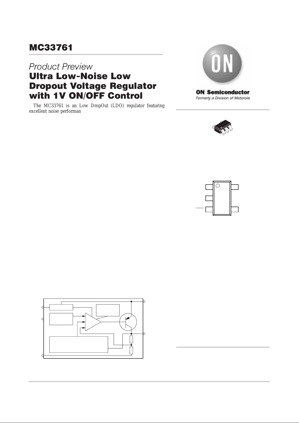
Simplified Block Diagram
Thermal
Shutdown
On/Off
Band Gap
Reference
*Current Limit
*Antisaturation Protection
*Load Transient Improvement
V
out
V
in
GND
NC
ON/
OFF
5
1
2
4
3
This document contains information on a product under development. ON Semiconductor
reserves the right to change or discontinue this product without notice.
TSOP–5
SN SUFFIX
CASE 483
1
http://onsemi.com
5
PIN CONNECTIONS AND
MARKING DIAGRAM
1
3
NC
V
in
2
GND
ON/OFF
4
V
out
5
See detailed ordering and shipping information in the package
dimensions section on page 1 1 of this data sheet.
ORDERING INFORMATION
LxxYW
xx = Version
YW = Date Code
(Top View)
Page 2
MC33761
http://onsemi.com
2
PIN FUNCTION DESCRIPTIONS
Pin # Pin Name Function Description
1 V
in
Powers the IC A positive voltage up to 12V can be applied upon this pin.
2 GND The IC’s ground
3 ON/OFF Shuts or
wakes–up the IC
A 900mV level on this pin is sufficient to start the IC. A 150mV shuts it down.
4 NC None It makes no arm to connect the pin to a known potential, like in a pin–to–pin
replacement case.
5 V
out
Delivers the
output voltage
This pin requires a 1µF output capacitor to be stable.
MAXIMUM RATINGS
Value
Rating Pin # Symbol Min Max Unit
Power Supply Voltage 1 V
in
— 12 V
ESD Capability, HBM Model All Pins 1 kV
ESD Capability, Machine Model All Pins 200 V
Maximum Power Dissipation
NW Suffix, Plastic Package
Thermal Resistance Junction–to–Air
P
D
R
q
J–A
Internally
Limited
210
W
°C/W
Operating Ambient Temperature
Maximum Junction Temperature
(1)
Maximum Operating Junction Temperature
(2)
T
A
T
Jmax
T
J
–40 to +85
150
125
°C
°C
°C
Storage Temperature Range T
stg
–60 to +150 °C
(1) Internally Limited by Shutdown.
(2) Specifications are guaranteed below this value.
ELECTRICAL CHARACTERISTICS
(For Typical Values TA = 25°C, for Min/Max values TA = –40°C to +85°C, Max TJ = 125°C unless otherwise noted)
Characteristics
Pin # Symbol Min Typ Max Unit
Logic Control Specifications
Input Voltage Range 3 V
ON/OFF
0 V
in
V
ON/OFF Input Resistance (all versions) 3 R
ON/OFF
250
k
W
ON/OFF Control Voltages
(3)
Logic Zero, OFF State, IO = 50 mA
Logic One, ON State, IO = 50 mA
3 V
ON/OFF
900
150
mV
Currents Parameters
Current Consumption in OFF State (all versions)
OFF Mode Current: Vin = V
out
+ 1 V, IO = 0, V
OFF
= 150 mV
IQ
OFF
0.1 2
m
A
Current Consumption in ON State (all versions)
ON Mode Current: Vin = V
out
+ 1 V , IO = 0, VON = 3.5 V
IQ
ON
180
m
A
Current Consumption in ON State (all versions), ON Mode
Saturation Current: Vin = V
out
– 0.5 V , No Output Load
IQ
SAT
800
m
A
Current Limit Vin = Vout
nom
+ 1 V,
Output is brought to Vout
nom
– 0.3 V (all versions)
I
MAX
100 180 mA
(3) Voltage Slope should be Greater than 2 mV/ms
Page 3
MC33761
http://onsemi.com
3
ELECTRICAL CHARACTERISTICS
(For Typical Values TA = 25°C, for Min/Max values TA = –40°C to +85°C, Max TJ = 125°C unless otherwise noted)
Characteristics
Pin # Symbol Min Typ Max Unit
Output Voltages
V
out
+ 1 V < Vin < 6 V, TA = 25°C, 1 mA < I
out
< 80 mA
2.5 V
5 V
out
2.462 2.5 2.537 V
2.8 V 5 V
out
2.758 2.8 2.842 V
3.0 V 5 V
out
2.955 3.0 3.045 V
3.3 V 5 V
out
3.250 3.3 3.349 V
3.6 V 5 V
out
3.546 3.6 3.654 V
Other Voltages up to 5V Available in 50mV Increments Steps 5 V
out
–1.5 X +1.5 %
V
out
+ 1V < Vin < 6V, TA = –40°C to +85°C, 1m A < I
out
< 80mA
2.5 V
5 V
out
2.425 2.5 2.575 V
2.8 V 5 V
out
2.716 2.8 2.884 V
3.0 V 5 V
out
2.91 3.0 3.090 V
3.3 V 5 V
out
3.201 3.3 3.399 V
3.6 V 5 V
out
3.492 3.6 3.708 V
Other Voltages up to 5V Available in 50mV Increments Steps 5 V
out
–3 X +3 %
Line and Load Regulation, Dropout Voltages
Line Regulation (all versions)
V
out
+ 1 V < Vin < 12 V, I
out
= 80 mA
5/1 Reg
line
20 mV
Load Regulation (all versions)
Vin = V
out
+ 1 V, C
out
= 1 mF, I
out
= 1 to 80 mA
5 Reg
load
40 mV
Dropout Voltage (all versions)
(3)
I
out
= 30 mA
I
out
= 60 mA
I
out
= 80 mA
5
5
5
Vin–V
out
Vin–V
out
Vin–V
out
90
140
160
150
200
250
mV
Dynamic Parameters
Ripple Rejection (all versions)
Vin = V
out
+ 1 V + 1 kHz 100 mVpp Sinusoidal Signal
5/1 Ripple –70 dB
Output Noise Density @ 1 kHz 5 150 nV/
√Hz
RMS Output Noise Voltage (all versions)
C
out
= 1 mF, I
out
= 50 mA, F = 100 Hz to 1 MHz
5 Noise 35
m
V
Output Rise Time (all versions) C
out
= 1 mF, I
out
= 50 mA,
10% of Rising ON Signal to 90% of Nominal V
out
5 t
rise
40
m
s
Thermal Shutdown
Thermal Shutdown (all versions) 125 °C
(3) V
out
is brought to V
out
– 100 mV
Page 4

MC33761
http://onsemi.com
4
DEFINITIONS
Load Regulation
The change in output voltage for a change in output
current at a constant chip temperature.
Dropout Voltage
The input/output differential at which the regulator output
no longer maintains regulation against further reductions in
input voltage. Measured when the output drops 100mV
below its nominal value (which is measured at 1V
differential value). The dropout level is affected by the chip
temperature, load current and minimum input supply
requirements.
Output Noise Voltage
This is the integrated value of the output noise over a
specified frequency range. Input voltage and output current
are kept constant during the measurement. Results are
expressed in µVRMS.
Maximum Power Dissipation
The maximum total dissipation for which the regulator
will operate within its specs.
Quiescent Current
The quiescent current is the current which flows through
the ground when the LDO operates without a load on its
output: internal IC operation, bias etc. When the LDO
becomes loaded, this term is called the Ground current. It is
actually the difference between the input current (measured
through the LDO input pin) and the output current.
Line Regulation
The change in output voltage for a change in input voltage.
The measurement is made under conditions of low
dissipation or by using pulse technique such that the average
chip temperature is not significantly affected. One usually
distinguishes static line regulation or DC line regulation (a
DC step in the input voltage generates a corresponding step
in the output voltage) from ripple rejection or audio
susceptibility where the input is combined with a frequency
generator to sweep from a few hertz up to a defined
boundary while the output amplitude is monitored.
Thermal Protection
Internal thermal shutdown circuitry is provided to protect
the integrated circuit in the event that the maximum junction
temperature is exceeded. When activated at typically 125°C,
the regulator turns off. This feature is provided to prevent
catastrophic failures from accidental overheating.
Maximum Package Power Dissipation
The maximum power package power dissipation is the
power dissipation level at which the junction temperature
reaches its maximum operating value, i.e. 125°C.
Depending on the ambient temperature, it is possible to
calculate the maximum power dissipation and thus the
maximum available output current.
Page 5

MC33761
http://onsemi.com
5
Characterization Curves
All curves taken with Vin = V
out
+ 1 V, V
out
= 2.8 V, C
out
= 1 mF
25°C
–40°C
25°C
85°C
Figure 1. Ground Current versus
Output Current
Figure 2. Quiescent Current versus
Temperature
Figure 3. Dropout versus Output Current Figure 4. Output Voltage versus
Output Current
OUTPUT CURRENT (mA)
4.5
4.0
3.5
3.0
2.5
2.0
1.5
1.0
10080600
GROUND CURRENT (mA)
AMBIENT TEMPERATURE (°C)
100806040200–20–40–60
180
175
170
m
QUIESCENT CURRENT ( A)
165
0.5
0
185
40
20
OUTPUT CURRENT (mA)
200
150
100
50
10080600
DROPOUT (mV)
OUTPUT CURRENT (mA)
100806040200
2.800
2.795
2.790
OUTPUT VOLTAGE (V)
2.775
0
2.805
4020
2.785
2.780
Figure 5. Dropout versus Temperature
TEMPERATURE (°C)
180
160
120
100
60
40
1008060–60
DROPOUT VOL TAGE (mV)
20
0
0
–20
80
140
–40 4020
–40°C
25°C
85°C
–40°C
85°C
40°C
–20°C
0°C
1 mA
30 mA
60 mA
80 mA
Page 6

MC33761
http://onsemi.com
6
APPLICATION HINTS
Input Decoupling
As with any regulator, it is necessary to reduce the
dynamic impedance of the supply rail that feeds the
component. A 1µF capacitor either ceramic or tantalum is
recommended and should be connected close to the
MC33761 package. Higher values will correspondingly
improve the overall line transient response.
Output Decoupling
Thanks to a novel concept, the MC33761 is a stable
component and does not require any specific Equivalent
Series Resistance (ESR) neither a minimum output current.
Capacitors exhibiting ESRs ranging from a few mW up to
3W can thus safely be used. The minimum decoupling value
is 1µF and can be augmented to fulfill stringent load
transient requirements. The regulator accepts ceramic chip
capacitors as well as tantalum devices.
Noise Decoupling
Unlike other LDOs, the MC33761 is a true low—noise
regulator. W ithout the need of an external bypass capacitor,
it typically reaches the incredible level of 40µVRMS overall
noise between 100 Hz and 100 kHz. To give maximum
insight on noise specifications, ON Semiconductor includes
spectral density graphics. The classical bypass capacitor
impacts the start—up phase of standard LDOs. However,
thanks to its low—noise architecture, the MC33761
operates without a bypass element and thus offers a typical
40µs start—up phase.
Protections
The MC33761 hosts several protections, giving natural
ruggedness and reliability to the products implementing the
component. The output current is internally limited to a
maximum value of 180 mA typical while temperature
shutdown occurs if the die heats up beyond 125°C. These
values let you assess the maximum differential voltage the
device can sustain at a given output current before its
protections come into play .
The maximum dissipation the package can handle is given
by:
P
max
+
T
Jmax
*
T
A
R
q
JA
If T
Jmax
is limited to 125°C, then the MC33761 can
dissipate up to 470mW @ 25°C. The power dissipated by the
MC33761 can be calculated from the following formula:
Ptot
+ǒVin
I
gnd
(I
out
)Ǔ)ǒVin*
V
out
Ǔ
I
out
or
Vin
max
+
Ptot)V
out
I
out
I
gnd
)
I
out
If a 80mA output current is needed, the ground current is
extracted from the data–sheet curves: 4mA @ 80mA. For a
MC33761SNT1–28 (2.8 V) delivering 80mA and operating
at 25°C, the maximum input voltage will then be 8.3V.
Typical Applications
The following picture portrays the typical application of
the MC33761.
Figure 6.
Page 7

MC33761
http://onsemi.com
7
Figure 7. A Typical Application Schematic
1
3
2
4
5
MC33761
R1
100 k
On/Off
+
C3
1 mF
+
C2
1 mF
Dropout Charge
Output
Permanently
Enables the IC
When Closed
Input
As for any low noise designs, particular care has to be
taken when tackling Printed Circuit Board (PCB) layout.
The figure below gives an example of a layout where stray
inductances/capacitances are minimized. This layout is the
basis for the MC33761 performance evaluation board. The
BNC connectors give the user an easy and quick evaluation
mean.
Page 8

MC33761
http://onsemi.com
8
Understanding the Load Transient Improvement
The MC33761 features a novel architecture which allows
the user to easily implement the regulator in burst systems
where the time between two current shots is kept very small.
The quality of the transient response time is related to
many parameters, among which the closed–loop bandwidth
with the corresponding phase margin plays an important
role. However, other characteristics also come into play like
the series pass transistor saturation. When a current
perturbation suddenly appears on the output, e.g. a load
increase, the error amplifier reacts and actively biases the
PNP transistor. During this reaction time, the LDO is in
open–loop and the output impedance is rather high. As a
result, the voltage brutally drops until the error amplifier
effectively closes the loop and corrects the output error.
When the load disappears, the opposite phenomenon takes
place with a positive overshoot. The problem appears when
this overshoot decays down to the LDO steady–state value.
During this decreasing phase, the LDO stops the PNP bias
and one can consider the LDO asleep (figure 8). If by
misfortune a current shot appears, the reaction time is
incredibly lengthened and a strong undershoot takes place.
This reaction is clearly not acceptable for line sensitive
devices, such as VCOs or other Radio–Frequency parts.
This problem is dramatically exacerbated when the output
current drops to zero rather than a few mA. In this later case,
the internal feedback network is the only discharge path,
accordingly lengthening the output voltage decay period
(figure 9).
The MC33761 cures this problem by implementing a
clever design where the LDO detects the presence of the
overshoot and forces the system to go back to steady–state
as soon as possible, ready for the next shot. Figure 10 and
11 show how it positively improves the response time and
decreases the negative peak voltage.
Figure 8. A standard LDO behavior when the load
current disappears
Figure 9. A standard LDO behavior when the load
current appears in the decay zone
Figure 10. Without load transient improvement Figure 11. MC33761 with load transient improvement
Page 9

MC33761
http://onsemi.com
9
MC33761 has a fast start–up phase
Thanks to the lack of bypass capacitor the MC33761 is
able to supply its downstream circuitry as soon as the OFF
to ON signal appears. In a standard LDO, the charging time
of the external bypass capacitor hampers the response time.
A simple solution consists in suppressing this bypass
element but, unfortunately, the noise rises to an
unacceptable level. MC33761 offers the best of both worlds
since it no longer includes a bypass capacitor and starts in
less than 40µs typically (Repetitive at 200Hz). It also
ensures a low–noise level of 40µVRMS 100Hz–100kHz.
The following picture details the typical 33761 startup
phase.
Figure 12. Repetitive start–up waveforms
Page 10

MC33761
http://onsemi.com
10
TYPICAL TRANSIENT RESPONSES
Figure 13. Output is pulsed from 2mA to 80mA Figure 14. Discharge effects from 0 to 40mA
Figure 15. Load transient improvement effect Figure 16. Load transient improvement effect
Page 11

MC33761
http://onsemi.com
11
TYPICAL TRANSIENT RESPONSES
Figure 17. MC33761 Typical Noise Density Performance
Figure 18. MC33761 Typical Ripple Rejection
Performance
Figure 19. Typical Output Impedance plot
C
out
= 1µF, Vin = V
out
+ 1
f, FREQUENCY (Hz)
0
–10
–20
–30
–50
–60
–70
–80
1,000,000100,000100
(dB)
f, FREQUENCY (Hz)
1,000,00010,0001,000100
2.5
1.0
0.5
Z
0
–90
–100
3.5
10,000
1,000
f, FREQUENCY (Hz)
100,00010,0001,000100
150
100
50
nV/sqrt Hz
0
250
100,000
1.5
2.0
3.0
(OHMS)
O
IO = 1 mA
10 mA
20 mA
80 mA
–40
IO = 50 mA
10 mA
1,000,000
200
IO = 50 mA
10 mA
Vin = VO + 1 V
TA = 25°C
C
out
= 1 mF
Vin = V
out
+ 1 V
TA = 25°C
C
out
= 1 mF
RMS Noise, IO = 10 mA:
20 Hz – 100 kHz: 29 mV
20 Hz – 1 MHz: 31 mV
RMS Noise, IO = 50 mA:
20 Hz – 100 kHz: 27 mV
20 Hz – 1 MHz: 30 mV
ORDERING INFORMATION
Device Voltage Output Package Shipping
MC33761SNT1–25 2.5V TSOP–5 3000 Units / Tape & Reel
MC33761SNT1–28 2.8V TSOP–5 3000 Units / Tape & Reel
MC33761SNT1–30 3.0V TSOP–5 3000 Units / Tape & Reel
Page 12

MC33761
http://onsemi.com
12
P ACKAGE DIMENSIONS
NOTES:
1. DIMENSIONING AND TOLERANCING PER ANSI
Y14.5M, 1982.
2. CONTROLLING DIMENSION: MILLIMETER.
3. MAXIMUM LEAD THICKNESS INCLUDES LEAD
FINISH THICKNESS. MINIMUM LEAD THICKNESS
IS THE MINIMUM THICKNESS OF BASE
MATERIAL.
DIM MIN MAX MIN MAX
INCHESMILLIMETERS
A 2.90 3.10 0.1142 0.1220
B 1.30 1.70 0.0512 0.0669
C 0.90 1.10 0.0354 0.0433
D 0.25 0.50 0.0098 0.0197
G 0.85 1.00 0.0335 0.0413
H 0.013 0.100 0.0005 0.0040
J 0.10 0.26 0.0040 0.0102
K 0.20 0.60 0.0079 0.0236
L 1.25 1.55 0.0493 0.0610
M 0 10 0 10
S 2.50 3.00 0.0985 0.1181
0.05 (0.002)
123
54
S
A
G
L
B
D
H
C
K
M
J
___ _
TSOP–5
SN SUFFIX
PLASTIC PACKAGE
CASE 483–01
ISSUE A
ON Semiconductor and are trademarks of Semiconductor Components Industries, LLC (SCILLC). SCILLC reserves the right to make changes
without further notice to any products herein. SCILLC makes no warranty , representation or guarantee regarding the suitability of its products for any particular
purpose, nor does SCILLC assume any liability arising out of the application or use of any product or circuit, and specifically disclaims any and all liability ,
including without limitation special, consequential or incidental damages. “Typical” parameters which may be provided in SCILLC data sheets and/or
specifications can and do vary in different applications and actual performance may vary over time. All operating parameters, including “Typicals” must be
validated for each customer application by customer’s technical experts. SCILLC does not convey any license under its patent rights nor the rights of others.
SCILLC products are not designed, intended, or authorized for use as components in systems intended for surgical implant into the body, or other applications
intended to support or sustain life, or for any other application in which the failure of the SCILLC product could create a situation where personal injury or
death may occur. Should Buyer purchase or use SCILLC products for any such unintended or unauthorized application, Buyer shall indemnify and hold
SCILLC and its officers, employees, subsidiaries, affiliates, and distributors harmless against all claims, costs, damages, and expenses, and reasonable
attorney fees arising out of, directly or indirectly , any claim of personal injury or death associated with such unintended or unauthorized use, even if such claim
alleges that SCILLC was negligent regarding the design or manufacture of the part. SCILLC is an Equal Opportunity/Affirmative Action Employer .
PUBLICATION ORDERING INFORMATION
ASIA/PACIFIC: LDC for ON Semiconductor – Asia Support
Phone: 303–675–2121 (Tue–Fri 9:00am to 1:00pm, Hong Kong Time)
Email: ONlit–asia@hibbertco.com
JAPAN: ON Semiconductor, Japan Customer Focus Center
4–32–1 Nishi–Gotanda, Shinagawa–ku, T okyo, Japan 141–8549
Phone: 81–3–5487–8345
Email: r14153@onsemi.com
ON Semiconductor Website: http://onsemi.com
For additional information, please contact your local Sales Representative.
MC33761/D
USA/EUROPE Literature Fulfillment:
Literature Distribution Center for ON Semiconductor
P.O. Box 5163, Denver, Colorado 80217 USA
Phone: 303–675–2175 or 800–344–3860 T oll Free USA/Canada
Fax: 303–675–2176 or 800–344–3867 Toll Free USA/Canada
Email: ONlit@hibbertco.com
Fax Response Line*: 303–675–2167
800–344–3810 Toll Free USA/Canada
*To receive a Fax of our publications
N. America Technical Support: 800–282–9855 Toll Free USA/Canada
 Loading...