

Page 1
. . . with single conversion circuitry including oscillator, mixer, IF amplifiers,
limiting IF circuitry, and quadrature discriminator. The MC3374 is perfect for
narrowband audio and data applications up to 75 MHz which require
extremely low power consumption. Battery powered applications down to
VCC = 1.1 V are possible. The MC3374 also includes an on–board voltage
regulator, low battery detection circuitry, a receiver enable allowing a power
down Sleep–Mode, two undedicated buffer amplifiers to allow
simultaneous audio and data reception, and a comparator for enhancing
FSK (Frequency Shift Keyed) data reception to 1200 baud.
• Low Supply Voltage: V
• Low Power Consumption: P
• Input Bandwidth 75 MHz
• Excellent Sensitivity: 0.5 µVrms for 12 dB SINAD
• Voltage Regulator A vailable (Source Capability 3.0 mA)
• Receiver Enable to Allow Active/Standby Operation
• Low Battery Detection Circuitry
• Self Biasing Audio Buffer
• Data Buffer
• FSK Data Shaping Comparator
• Standard 32–Lead QFP Surface Mount Package
Sleep–Mode is a trademark of Motorola, Inc.
= 1.1 to 3.0 Vdc
CC
= 1.5 to 5.0 mW
D
Order this document by MC3374/D
LOW VOLTAGE
SINGLE CONVERSION
FM RECEIVER
SEMICONDUCTOR
TECHNICAL DATA
32
1
FTB SUFFIX
PLASTIC PACKAGE
CASE 873
(Thin QFP)
ORDERING INFORMATION
Tested Operating
Device
MC3374FTB TA = –10° to +70°C TQFP–32
Temperature Range
Package
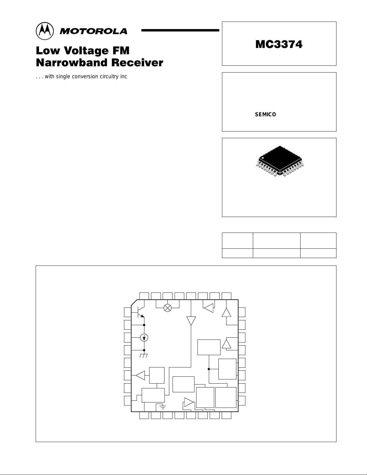
IF Gnd
V
CC2
1
2
3
4
5
6
7
8
Osc Base
Osc Emit
Isrc Dcpl
Rec Audio
Demodulator Decoupling
Quad T ank
*Internal Connection, do not ground.
Simplified Block Diagram
Data
Osc
MixerInMixer
Dcpl
32 31 30 29 28 27 26 25
Low
Pass
Output
Buffer
Filter
Quadrature
Demodulator
9 101112131415 16
Quad
Demod
T ank
Gnd
This device contains 87 active transistors
Mixer
Dcpl
2nd IF
Main
Current
Reference
Comp.
2nd IF
In
I/P
Out
Mixer
*N/C *N/C Comp
Buffer
Out
Data
Buffer
Voltage
Reference
Receiver
Enable
Comp
O/P
Enable
Data
Buffer
Rec
1st IF
In
1st IF
Audio
Buffer
Battery
Detector
Voltage
Reference
Regulator
Reference
Out
Low
T est
24
V
CC3
23
1st IF In
22
Audio Buffer Out
21
Audio Buffer In
20
Low Battery Detector
19
1.2 V Select
V
18
CC
17
V
reg
MOTOROLA ANALOG IC DEVICE DATA
Motorola, Inc. 1996 Rev 0
1
Page 2
MC3374
MAXIMUM RATINGS
Supply Voltage 18 5.0 Vdc
RF Input Signal 31 1.0 Vrms
Audio Buffer Input 21 1.0 Vrms
Data Buffer Input 26 1.0 Vrms
Comparator Input 13 1.0 Vrms
Junction Temperature – 150 °C
Storage Temperature – –65 to +150 °C
Device should not be operated at or outside these values. The “Recommended Operating Limits” provide
for actual device operation.
RECOMMENDED OPERATING CONDITIONS
Supply Voltage 18 1.1 to 3.0 Vdc
Receiver Enable Voltage 15 V
1.2 V Select Voltage 19 Open or V
RF Input Signal Level 31 0.001 to 100 mVrms
RF Input Frequency 31 0 to 75 MHz
Intermediate Frequency (IF) – 455 kHz
Audio Buffer Input 21 0 to 75 mVrms
Data Buffer Input 26 0 to 75 mVrms
Comparator Input 13 10 to 300 mVrms
Ambient Temperature – –10 to 70 °C
(Voltage with respect to Pins 4 and 10; TA = 25°C.)
Rating Pin Value Unit
Parameter Pin Value Unit
CC
CC
Vdc
Vdc
ELECTRICAL CHARACTERISTICS (V
Circuit of Figure 1, unless otherwise noted.)
Characteristic
OVERALL MC3374 PERFORMANCE
Drain Current – Pin 15 = VCC (Enabled)
Drain Current – Pin 15 = 0 Vdc (Disabled)
Recovered Audio (RF Input = 10 µV) 6 13 18 30 mVrms
Noise Output (RF Input = 0 mV, 300 Hz–5.0 kHz) 6 – 1.0 – mVrms
Input for –ā3.0 dB Limiting
MIXER
Mixer Input Resistance (Rp) 31 – 1.5 – kΩ
Mixer Input Capacitance (Cp) 31 – 9.0 – pF
FIRST IF AMPLIFIER
First IF Amp Voltage Gain – – 27 – dB
AUDIO BUFFER
Voltage Gain – 3.0 4.0 4.7 V/V
Input Resistance 21 – 110 – kΩ
Maximum Input for Undistorted Output (<5% THD) 21 – 64 – mVrms
Maximum Output Swing (<5% THD) 22 – 690 – mV
Output Resistance 22 – 780 – Ω
DATA BUFFER
Voltage Gain – 1.4 2.7 4.3 V/V
Input Resistance 26 – 9.8 – MΩ
Maximum Input for Undistorted Output (<5% THD) 26 – 100 – mV rms
Maximum Output Swing (<5% THD) 27 – 800 – mV
Output Resistance 27 – 690 – Ω
= 1.3 V, fo = 10.7 MHz, f
CC
= 1.0 kHz, Deviation = 3.0 kHz, TA = 25°C, Test
mod
Pin Min Typ Max Unit
5 + 18 + 24
5 + 18 + 24
31 – 0.6 – µVrms
–
–
1.6
0.5
3.0
–
mA
µA
pp
pp
2
MOTOROLA ANALOG IC DEVICE DATA
Page 3
MC3374
ELECTRICAL CHARACTERISTICS (continued) (V
= 1.3 V, fo = 10.7 MHz, f
CC
= 1.0 kHz, Deviation = 3.0 kHz, T
mod
A
= 25°C, Test Circuit of Figure 1, unless otherwise noted.)
Characteristic
Pin Min Typ Max Unit
COMPARATOR
Minimum Input for Triggering (RL = 100 kΩ) 13 – 7.0 – mVrms
Maximum Input Frequency (RL = 100 kΩ) 13 – 25 – kHz
Rise Time (10–90%; RL = 100 kΩ) 14 – 5.0 – µs
Fall Time (90–10%; RL = 100 kΩ) 14 – 0.4 – µs
LOW BATTERY DETECTOR
Low Battery Trip Point 19 – 1.2 – Vdc
Low Battery Output – VCC = 0.9 V
Low Battery Output – VCC = 1.3 V
20
20
–
–
0.2
V
CC
–
Vdc
–
VOLTAGE REGULATOR
Regulated Output (see Figure 4) 17 0.95 1.07 1.15 Vdc
Source Capability 17 – – 3.0 mA
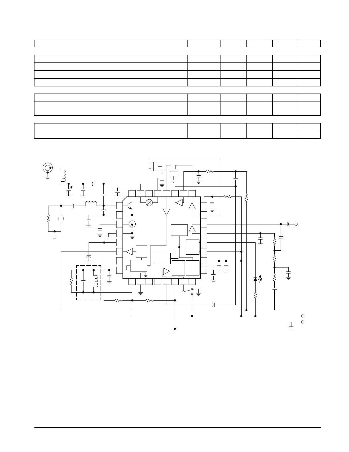
Figure 1. MC3374 Pager IF Application Circuit
RF Input
50
FL1
L1
C
XRD
56 k
C
C1
C2C1
L2
C3
C4
C
10
LC1 100 100 k
C
C2
C3
B
0.1
1
2
3
4
5
Output
6
7
8
C
B
C
32 31 30 29 28 27 26 25
Mixer
MC3374
Buffer
Low
Pass
Filter
Quadrature
Demodulator
9 10111213141516
N.C. N.C.
B
2nd IF
Main
Current
Reference
Comp.
FL2
Data
Buffer
Voltage
Reference
Receiver
Enable
1st IF
Audio
Buffer
Battery
Detector
Voltage
Reference
Enable
Low
0.01
24
23
22
21
20
19
18
17
Disable
180 k
– 330
0.1 10
1.0
4.7
+
0.1
39 k
0.1
µ
F
1.0
8.2 k
8.2 k
3.3 k
0.22
R
L
3900 P
0.022
Audio
Output
NOTES:
1.FL1 and FL2 are 455 kHz ceramic bandpass filters, which should
have input and output impedances of 1.5 kΩ to 2.0 kΩ. Suggested
part numbers are MuRata CFU455X or CFW455x – the ‘X’ suffix
denotes bandwidth.
2.LC1 is a 455 kHz LC resonator. Recommended part numbers are
T oko America RMC2A6597HM or 5SVLC–0637BGT (smaller).
The evaluation board layout shown provides for use of either
resonator. Ceramic discriminator elements cannot be used with
the MC3374 due to their low input impedance. The damping
resistor value can be raised to increase the recovered audio or
lowered to increase the quadrature detector’s bandwidth and
linearity – practical limits are approximately 27 kΩ to 75 kΩ.
Typically the quadrature detector’s bandwidth should match the
low IF filter’s bandwidth.
3.The data buffer is set up as a low–pass filter with a corner
frequency of approximately 200 Hz. The audio buffer is a
bandpass filter with corner frequencies of 300 Hz and 3.0 kHz.
The audio amplifier provides bass suppression.
MOTOROLA ANALOG IC DEVICE DATA
Data Output
V
CC
V
EE
4.CC1 and CC3 are RF coupling capacitors and should have ≤ 20 Ω
impedance at the desired input and oscillator frequencies.
5.CC2 provides “light coupling” of the oscillator signal into the mixer,
and should have a 3.0 kΩ to 5.0 kΩ impedance at the desired
local oscillator frequency.
6.Capacitors labelled CB are bypass capacitors and should have
20 Ω impedance at the desired RF and local oscillator frequencies.
7.The network of L1, C1 and C2 provides impedance matching of
the mixer input (nominally 3.0 kΩ shunted by 9.0 pF) to 50 Ω at the
desired RF/IF input frequency. This will allow for bench testing of
the receiver from typical RF signal generators or radio service
monitors, but additional or different matching will be required to
maximize receiver sensitivity when used in conjunction with an
antenna, RF preamplifier or mixer.
3
Page 4

MC3374
In. Freq. L1 L2 C1 C2 C3 C4 CC1/C
10.7 MHz 6.8 µH Short 2–82 pF 10 pF 120 pF 50 pF 1.0 nF 5.0 pF 0.1 µF Open
45 MHz 0.68 µH 1.2 µH 5–25 pF Open 30 pF 5.0 pF 1.0 nF 1.0 pF 1.0 nF 1.0 k
72 MHz 0.22 µH 0.22 µH 5–25 pF Open 18 pF 3.0 pF 470 pF 1.0 pF 470 pF 1.0 k
Figure 2. Recovered Audio versus Supply
60
50
40
30
20
RECOVERED AUDIO (mVrms)
10
0
0 1.0 2.0 3.0 4.0
VCC (V)
V
22
V
6
30
20
10
0
–10
–20
N, S+N (dB)
–30
–40
–50
–60
–120 – 1 10 –100 –90 –80 –70 –60 –50 –40 –30
C3
Figure 3. S+N, N versus Input
C
C2
INPUT (dBm)
S+N
N
C
B
RD
Figure 5. Regulated Output and Recovered
1200
Figure 4. V
1000
800
600
400
200
V17, VOLTAGE REGULATION (mV)
0
0 1.0 2.0 3.0 4.0 5.0
RL =
RL = 990
RL = 330
REG
∞
VCC (V)
versus Supply
Audio versus T emperature
1140
1120
1100
1080
1060
1040
V17, REGULATED OUTPUT (mVdc)
1020
1000
–50 – 25 0 25 50 75 100 125
TA, AMBIENT TEMPERATURE (°C)
V
17
V
6
18.0
17.5
17.0
16.5
16.0
15.5
15.0
14.5
V6, RECOVERED AUDIO (mV rms)
Figure 6. Buffer Amplifier Gains
versus T emperature
4.01
3.99
A
vdb
3.97
A
3.95
, AUDIO BUFFER GAIN (V/V)
3.93
vab
A
3.91
–50 –25 0 25 50 75 100 125
TA, AMBIENT TEMPERATURE (
4
vab
°
C)
MOTOROLA ANALOG IC DEVICE DATA
3.03
2.98
2.93
2.88
, DATA BUFFER GAIN (V/V)
2.83
vdb
A
2.78
Page 5

MC3374
Figure 7. MC3374 Pager Receiver PCB Artwork
COPPER 1 LAYER
(Actual View of Surface Mount Side)
RF Input V
Data
Output
EE
MC3374FTB
2.0
″
Enable
Disable
(Caution: Reversed View of Through–Hole Side)
V
CC
2.2
″
COPPER 2 LAYER
COMPONENT 1 LAYER COMPONENT 2 LAYER
L1
C2
C
C1
C
C1
C
C3
C4
4.7
NOTE: + = Through Hole
0.1
56 K
RD
C
C2
C3
B
100 K
CC
C
GND
C
B
B
1.0
1.0
0.1
3900 P
10
V
CC
GND
V
RF I/P
X
10
L2
0.01
39 k 180 k
LC1
Data O/P
SMA
FL1
0.01
LED
R
FL2
L
0.33 k
3.3 k
8.2 k
0.1
0.01
Enable
Disable
0.022
8.2 k
0.22
MOTOROLA ANALOG IC DEVICE DATA
5
Page 6

MC3374
CIRCUIT DESCRIPTION
The MC3374 is an FM narrowband receiver capable of
operation to 75 MHz. The low voltage design yields low
power drain and excellent sensitivity in narrowband voice
and data link applications. In the typical application the mixer
amplifies the incoming RF or IF signal and converts this
frequency to 455 kHz. The signal is then filtered by a 455 kHz
ceramic filter and applied to the first intermediate frequency
(IF) amplifier input, before passing through a second ceramic
filter. The modulated IF signal is then applied to the limiting IF
amplifier and detector circuitry. Modulation is recovered by a
conventional quadrature detector. The typical modulation
bandwidth available is 3.0 to 5.0 kHz.
Features available include buffers for audio/data
amplification and active filtering, on board voltage regulator,
low battery detection circuitry with programmable level, and
receiver disable circuitry. The MC3374 is an FM utility
receiver to be used for voice and/or narrowband data
reception. It is especially suitable where extremely low power
consumption and high design flexibility are required.
APPLICATION
The MC3374 can be used as a high performance FM IF for
the use in low power dual conversion receivers. Because of
the MC3374’s extremely good sensitivity (0.6 µV for 20 dB
(S+N/N, see Figure 3)), it can also be used as a stand alone
single conversion narrowband receiver to 75 MHz for
applications not sensitive to image frequency interference.
An RF preamplifier will likely be needed to overcome
preselector losses.
The oscillator is a Colpitts type which must be run under
crystal control. For fundamental mode crystals choose
resonators, parallel resonant, for a 32 pF load. For higher
frequencies, use a 3rd overtone series mode type. The coil
L2 and RD resistor are needed to ensure proper operation.
The best adjacent channel and sensitivity response occur
when two 455 kHz ceramic filters are used, as shown in
Figure 1. Either can be replaced by a 0.1 µF coupling
capacitor to reduce cost, but some degradation in sensitivity
and/or stability is suspected.
The detector is a quadrature type, with the connection
from the limiter output to the detector input provided
internally. A 455 kHz LC tank circuit must be provided
externally. One of the tank pins (Pin 8) must be decoupled
using a 0.1 µF capacitor. The 56 kΩ damping resistor (see
Figure 1), determines the peak separation of the detector
(and thus its bandwidth). Smaller values will increase the
separation and bandwidth but decrease recovered audio and
sensitivity.
The data buffer is a noninverting amplifier with a nominal
voltage gain of 2.7 V/V. This buffer needs its dc bias
(approximately 250 mV) provided externally or else
debiasing will occur. A 2nd order Sallen–Key low pass filter,
as shown in Figure 1, connecting the recovered audio output
to the data buffer input provides the necessary dc bias and
some post detection filtering. The buffer can also be used as
an active filter.
The audio buffer is a noninverting amplifier with a nominal
voltage gain of 4.0 V/V . This buf fer is self–biasing so its input
should be ac coupled. The two buffers, when applied as
active filters, can be used together to allow simultaneous
audio and very low speed data reception. Another possible
configuration is to receive audio only and include a
noise–triggered squelch.
The comparator is a noninverting type with an open
collector output. Typically, the pull–up resistor used between
Pin 14 and VCC is 100 kΩ. With RL = 100 kΩ the comparator
is capable of operation up to 25 kHz. The circuit is
self–biasing, so its input should be ac coupled.
The regulator is a 1.07 V reference capable of sourcing
3.0 mA. This pin (Pin 17) needs to be decoupled using a
1.0 – 10 µF capacitor to maintain stability of the MC3374.
All three VCCs on the MC3374 (VCC, V
the same supply voltage. VCC is typically decoupled using
capacitors only. V
the RC bypasses shown in Figure 1. Eliminating the resistors
on the V
applications, but a reduction in sensitivity and quieting will
likely occur.
The low battery detection circuit gives an NPN open
collector output at Pin 20 which drops low when the MC3374
supply voltage drops below 1.2 V . T ypically it would be pulled
up via a 100 kΩ resistor to supply.
The 1.2 V Select pin, when connected to the MC3374 supply,
programs the low battery detector to trip at VCC < 1.1 V. Leaving
this pin open raises the trip voltage on the low battery detector.
Pin 15 is a receiver enable which is connected to VCC for
normal operation. Connecting this pin to ground shuts off
receiver and reduces current drain to ICC < 0.5 µA.
CC2
and V
and V
CC2
bypasses may be possible in some
CC3
should be bypassed using
CC3
CC2
, V
CC3
) run on
APPENDIX
Design of 2nd Order Sallen–Key Low Pass Filters
+
C1
+
–
Avo = K
1
1
R1C1
)
0.707
Ǹ
(1–K)
R2C2
yields a maximally flat
Low Pass Output
0 to fo Hz
Input
The audio and data buffers can easily be configured as active
low pass filters using the circuit configuration shown above.
The circuit has a center frequency (fo) and quality factor (Q)
given by the following:
If possible, let R1 = R2 or C1 = C2 to simplify the above
equations. Be sure to avoid a negative Q value to prevent
instability . Setting
filter response.
R1
R2
C2
Bias
fo+
Q
+
R2C2
Ǹ
R1C1
Q+1ń2
Ǹ
2pR1R2C1C2
R1C2
Ǹ
)
R2C1
Ǹ
6
MOTOROLA ANALOG IC DEVICE DATA
Page 7

MC3374
Data Buffer Design Audio Buffer Design
The data buffer is designed as follows:
fo = 200 Hz
C1 = C2 = 0.01 µF
Q = 0.707 (target)
K = 2.7 (data buffer open loop voltage gain)
Setting C1 = C2 yields:
fo
+
Q
+
R2
Ǹ
R1
Iteration yields R2 = 4.2 (R1) to make Q = 0.707.
Substitution into the equation for fo yields:
R1 = 38 kΩ (use 39 kΩ)
R2 = 4.2(R1) = 180 kΩ
C1 = C2 = 0.01 µF
1
Ǹ
2pC1 R1R2
1
(2–K)
Ǹ
)
R1
R2
The audio buffer is designed as follows:
fo = 3000 Hz
R1 = R2 = 8.2 kΩ
Q = 0.707 (target)
K = 3.9 (audio buffer open loop voltage gain)
Setting C1 = C2 yields:
fo
+
Q
+
C2
Ǹ
C1
Iteration yields C2 = 2.65 (C1) to make Q = 0.707.
Substitution into the equation for fo yields:
C2 = 2.65(C1) = 0.01 µF
R1 = R2 = 8.2 kΩ
1
Ǹ
2pR1 C1C2
1
)
(1–K)
C1 = 3900 pF
Ǹ
C1
C2
Motorola reserves the right to make changes without further notice to any products herein. Motorola makes no warranty , representation or guarantee regarding
the suitability of its products for any particular purpose, nor does Motorola assume any liability arising out of the application or use of any product or circuit, and
specifically disclaims any and all liability, including without limitation consequential or incidental damages. “T ypical” parameters which may be provided in Motorola
data sheets and/or specifications can and do vary in different applications and actual performance may vary over time. All operating parameters, including “Typicals”
must be validated for each customer application by customer’s technical experts. Motorola does not convey any license under its patent rights nor the rights of
others. Motorola products are not designed, intended, or authorized for use as components in systems intended for surgical implant into the body, or other
applications intended to support or sustain life, or for any other application in which the failure of the Motorola product could create a situation where personal injury
or death may occur. Should Buyer purchase or use Motorola products for any such unintended or unauthorized application, Buyer shall indemnify and hold Motorola
and its officers, employees, subsidiaries, affiliates, and distributors harmless against all claims, costs, damages, and expenses, and reasonable attorney fees
arising out of, directly or indirectly, any claim of personal injury or death associated with such unintended or unauthorized use, even if such claim alleges that
Motorola was negligent regarding the design or manufacture of the part. Motorola and are registered trademarks of Motorola, Inc. Motorola, Inc. is an Equal
Opportunity/Affirmative Action Employer.
MOTOROLA ANALOG IC DEVICE DATA
7
Page 8

L
24 17
25
MC3374
OUTLINE DIMENSIONS
FTB SUFFIX
PLASTIC PACKAGE
CASE 873–01
(Thin QFP)
ISSUE A
16
L
-C-
SEATING
PLANE
-A-
DATUM
PLANE
C
-H-
S S
S S
-BB
DETAIL A
32
9
81
-DA
0.20 (0.008) A–B D
0.05 (0.002)
M
A–B
S S
C
V
M
0.20 (0.008) C A–B D
0.05 (0.002) A–B
M
B
B
P
0.20 (0.008) H A–B D
-A-,-B-,-D-
DETAIL A
BASE METAL
F
S
0.20 (0.008) A–B D
M
S S
H
M
DETAIL C
J
N
D
E
H
G
U
K
X
DETAIL C
M
NOTES:
1. DIMENSIONING AND TOLERANCING PER ANSI
Y14.5M, 1982.
2. CONTROLLING DIMENSION: MILLIMETER.
3. DATUM PLANE -H- IS LOCATED AT BOTTOM OF
T
R
Q
LEAD AND IS COINCIDENT WITH THE LEAD WHERE
THE LEAD EXITS THE PLASTIC BODY AT THE
BOTTOM OF THE PARTING LINE.
4. DATUMS -A-, -B- AND -D- TO BE DETERMINED AT
DATUM PLANE -H-.
5. DIMENSIONS S AND V TO BE DETERMINED AT
SEATING PLANE -C-.
6. DIMENSIONS A AND B DO NOT INCLUDE MOLD
PROTRUSION. ALLOWABLE PROTRUSION IS 0.25
(0.010) PER SIDE. DIMENSIONS A AND B DO
INCLUDE MOLD MISMATCH AND ARE DETERMINED
AT DATUM PLANE -H-.
7. DIMENSION D DOES NOT INCLUDE DAMBAR
PROTRUSION. ALLOWABLE DAMBAR PROTRUSION
SHALL BE 0.08 (0.003) TOTAL IN EXCESS OF THE D
DIMENSION AT MAXIMUM MATERIAL CONDITION.
DAMBAR CANNOT BE LOCATED ON THE LOWER
RADIUS OR THE FOOT.
DATUM
-H-
PLANE
0.01 (0.004)
0.20 (0.008) A–B D
M
S S
C
SECTION B-B
VIEW ROTATED 90° CLOCKWISE
MILLIMETERS INCHES
MIN MINMAX MAX
DIM
A
B
C
D
E
F
G
H
J
K
L
M
N
P
Q
R
S
T
U
V
X
7.10
6.95
7.10
6.95
1.60
1.40
0.373
0.273
1.50
1.30
—
0.273
0.80 BSC
0.20
—
0.197
0.119
0.57
0.33
5.6 REF
8
6
°
°
0.135
0.119
0.40 BSC
10
°
5
°
0.25
0.15
9.15
8.85
0.25
0.15
11
5
°
°
9.15
8.85
1.0 REF 0.039 REF
0.274
0.274
0.055
0.010
0.051
0.010
0.031 BSC
—
0.005
0.013
0.220 REF
6
°
0.005
0.016 BSC
5
°
0.006
0.348
0.006
5
°
0.348
0.280
0.280
0.063
0.015
0.059
0.008
0.008
0.022
0.005
10
0.010
0.360
0.010
11
0.360
8
—
°
°
°
How to reach us:
USA/EUROPE/Locations Not Listed: Motorola Literature Distribution; JAPAN: Nippon Motorola Ltd.; Tatsumi–SPD–JLDC, 6F Seibu–Butsuryu–Center,
P.O. Box 20912; Phoenix, Arizona 85036. 1–800–441–2447 or 602–303–5454 3–14–2 Tatsumi Koto–Ku, Tokyo 135, Japan. 03–81–3521–8315
MFAX: RMF AX0@email.sps.mot.com – TOUCHT ONE 602–244–6609 ASIA/P ACIFIC: Motorola Semiconductors H.K. Ltd.; 8B Tai Ping Industrial Park,
INTERNET: http://Design–NET.com 51 Ting Kok Road, Tai Po, N.T., Hong Kong. 852–26629298
8
◊
MOTOROLA ANALOG IC DEVICE DATA
MC3374/D
*MC3374/D*
 Loading...