

Page 1
MOTOROLA
SEMICONDUCTOR TECHNICAL
Standalone Tag Reader Circuit
Order this document
by MC33690/D
MC33690
STANDALONE
STARC
The Standalone Tag Reader Circuit (STARC) is an integrated
circuit dedicated to the automotive immobilizer applications. It
combines on the same chip all the circuitry to interface with a
transponder : antenna drivers and demodulator.
A low dropout voltage regulator and a physical interface fully
compatible with the ISO 9141 norm are also available.
The Standalone Tag Reader Circuit is fabricated with the
SMARTMOS
metal, 1.4µm, 45V technology, combining CMOS and bipolar
devices.
• Contactless 125kHz tag reader module :
- Self synchronous sample & hold demodulator
- Amplitude or phase modulation detection
- High sensitivity
- Fast “read after write“ demodulator settling time
- Low resistance and high current antenna drivers :
2Ω @ 150mA (typ.)
- Bidirectionnal data transmission
- Multi tag, multi scheme operation.
• Low dropout voltage regulator :
- Wide input supply voltage range :
from 5.5V up to 40V
- Output current capability up to 150mA DC with an
external power transistor
- 5V output voltage with a ± 5% accuracy
- Low voltage reset function
- Low current consumption in standby mode :
300µA (typ.).
• ISO 9141 transmitter and receiver module :
- Input voltage thresholds ratiometric to the supply
voltage
- Current limitation
- Ouput slew rate control
- No external protection device required.
TM
3.5 technology. This process is a double layer
TAG READER
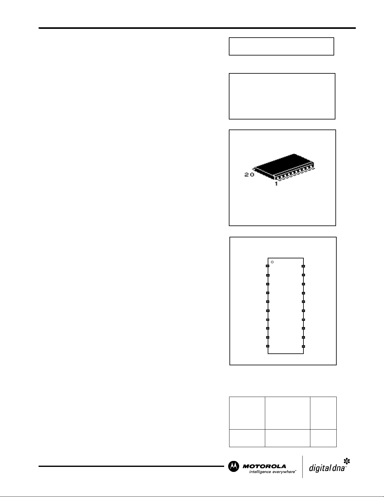
CIRCUIT
DW SUFFIX
Plastic Package
CASE 751D
SO - 20
Pin Connections
VSUP
SOURCE
GATE
TD1
VSS
VDD
TD2
MODE1
MODE2
1
2
3
4
5
6
7
8
9
RD
ORDERING INFORMATION
Tx
20
19
Rx
18
K
17
AM
XTAL1
16
XTAL2
15
14
LVR
13
DOUT
12
CEXT
1110
AGND
This document contains information on a new product under development. Motorola
reserves the right to change or discontinue this product without notice.
REV 4.8
© Motorola, Inc., 2002.
Device
MC33690DW
Operating
Junction
Tem p e r a t ure
Range
= -40°C to
T
J
125°C
Package
SOIC 20
Page 2
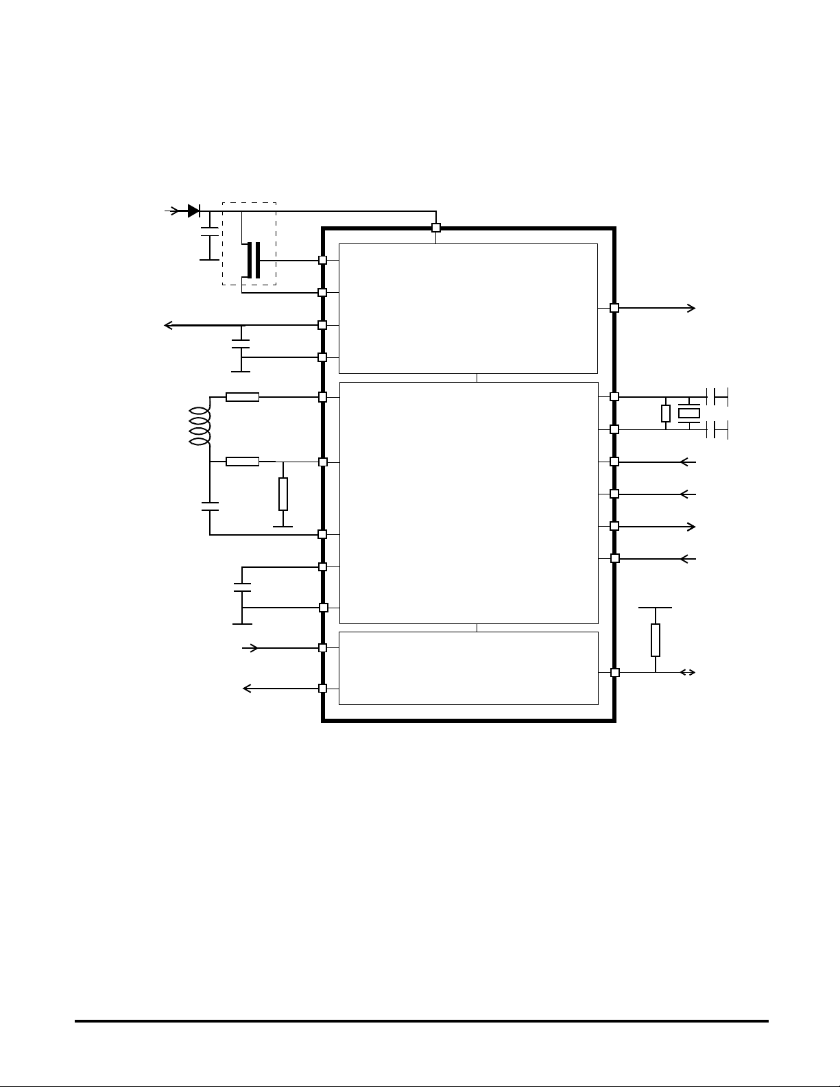
BLOCK DIAGRAM
Optional : external N channel MOS required for sourced current > 50mA.
A recommended reference is MMFT 3055VL from Motorola.
MC33690
Figure 1 : Standalone Tag Reader Circuit
VBAT
VDD
VSUP
C
1
GATE
SOURCE
VDD
10µF
VSS
R
A
L
A
R
1
C
A
C
EXT
10nF
TD1
RD
R
2
TD2
CEXT
AGND
Tx
Voltage Regulator
Tag Reader
LVR
8MHz
XTAL1
XTAL2
MODE1
MODE2
DOUT
AM
VBAT
510Ω
ISO 9141 Interface
Rx
K
© Motorola, Inc., 2002.
MOTOROLA SEMICONDUCTORS PRODUCTS
2
revision 4.8, 5 February 2002
Page 3
MAXIMUM RATINGS
Supply voltage V
Supply voltage without using the voltage regulator
(V
= VDD)
SUP
Voltage on SOURCE V
Current into/from GATE 0 mA
MC33690
Rating Symbol Value Unit
VSS-0.3 to +40 V
VSS-0.3 to +7 V
-0.3 to +40 V
SS
V
SUP
DD
Voltage on GATE V
Voltage on pins :
MODE1/2, CEXT, DOUT, LVR, XTAL1/2, Rx, Tx
Voltage on RD ±10 V
Voltage on K and AM V
Current on TD1 & TD2
(Drivers on & off)
Voltage on AGND VSS±0.3 V
ESD voltage capability (HBM, see note 1) ±2000 V
ESD voltage capability (MM, see note 1) ±200 V
Solder heat resistance test (10s) 260 °C
Junction temperature T
Storage temperature T
Note 1 :
Human Body model, AEC-Q100-002 Rev. C.
Machine Model, AEC-Q100-003 Rev. E.
THERMAL CHARACTERISTIC
-0.3 V
SS
V
SS
-0.3 to V
-3 to 40 V
SS
+0.3 V
DD
±300 mA
J
s
170 °C
-65 to +150 °C
Junction to ambiant thermal resistance (SOIC20) R
© Motorola, Inc., 2002.
Characteristic Symbol Value Unit
th
MOTOROLA SEMICONDUCTORS PRODUCTS
80 °C/W
revision 4.8, 5 February 2002
3
Page 4

PIN FUNCTION DESCRIPTION
Pin Function Description
1 VSUP Power supply
2 SOURCE External N channel transistor source
3 GATE External N channel transistor gate
4 TD1 Antenna driver 1 output
5 VSS Power and digital ground
6 VDD Voltage regulator output
7 TD2 Antenna driver 2 output
8 MODE1 Mode selection input 1
9 MODE2 Mode selection input 2
10 RD Demodulator input
11 AGND Demodulator ground
12 CEXT Comparator reference input
MC33690
13 DOUT Demodulator output (5V)
14 LVR Low Voltage Reset input/output
15 XTAL2 Oscillator output
16 XTAL1 Oscillator input
17 AM Amplitude modulation input
18 K ISO 9141 transmitter output and receiver input
19 Rx ISO 9141 receiver monitor output
20 Tx ISO 9141 transmitter input
© Motorola, Inc., 2002.
MOTOROLA SEMICONDUCTORS PRODUCTS
4
revision 4.8, 5 February 2002
Page 5
DESCRIPTION
TAG READER MODULE
MC33690
The Tag Reader module is dedicated for
automotive or industrial applications where
information has to be transmitted contactless.
The tag reader module is a write/read (challenge/
response) controller for applications which
demand high security level.
The tag reader module is connected to a serial
tuned LC circuit which generates a magnetic field
power supplying the tag.
Figure 2 : Tag Reader block diagram
R
A
TD1
L
A
125kHz
C
A
1/32 counter 1/2
125kHz
Self synchronous
sample & hold
The use of a synchronous sample & hold
technique allows communication with all
avalaible tags using admittance switching
producing absorption of the RF field.
Load amplitude or phase shift modulation can be
detected at high bit rates up to 8kHz.
125kHz is the typical operational carrier
frequency of the tag reader module with a 8MHz
clock.
AM Data
Clock 8MHz
4MHz
8MHz
Shutdown
Setup & Preload
LVR
TD2
R
1
R
2
-
+
VDD
RD
11.25° , 22.5° , 33.75° , 45° , 56.25° , 67.5° , 78.75° , 90°
+ 0°, -11.25°, -22.5°, -33.75°, -45°, -56.25°, -67.5°, -78.75°
Buffer
500ns
S/H Buffer
+
-
AGND
100K
C
EXT
Comparator
+
Ω
-
VDD
CEXT
10nF
DCQ
500µA
Interface
Data out
© Motorola, Inc., 2002.
MOTOROLA SEMICONDUCTORS PRODUCTS
5
revision 4.8, 5 February 2002
Page 6
MC33690
Read function
When answering to the base station, a
transponder generates an absorption modulation
of the magnetic field. It results in an amplitude/
phase modulation of the current across the
antenna. This information is picked up at the
antenna tap point between the coil and the
capacitor. An external resistive ladder down
scales this voltage to a level compatible with the
demodulator input voltage range (see parameter
V
page 16).
INRD
The demodulator (see figure 2) consists of :
- an input stage (emitter follower),
- a sample & hold circuit,
- a voltage follower,
- a low offset voltage comparator.
The sampling time is automatically set to take
into account a phase shift due to the tolerances
of the antenna components (L and C) and of the
oscillator. The allowed phase shift measured at
the input RD ranges from -45° to +45°. Assuming
that the phase reference is the falling edge of the
driving signal TD1, this leads to a sampling time
phase ranging from -78.75° to 90° with discrete
steps of 11.25°. After reset condition, the
sampling time phase is +11.25°.
The antenna phase shift evaluation is only
done :
- after each wake-up command (see pages
10 to 12),
- or after reset (see page 7).
This is necessary to obtain the best demodulator
performances.
In order to ensure a fast demodulator settling
time after wake up, reset or a write sequence, the
external capacitor C
is preloaded at its
EXT
working voltage.
This preset occurs 256µs after switching the
antenna drivers on and its duration is 128µs.
After wake up or reset, the preset has the same
duration but begins 518µs after clock settling.
After power on reset, VSUP must meet the
minimum specified value, enabling the nominal
operation of VDD, before the start of the preset.
Otherwise the preset must be done by the user
through a standby/wake-up sequence.
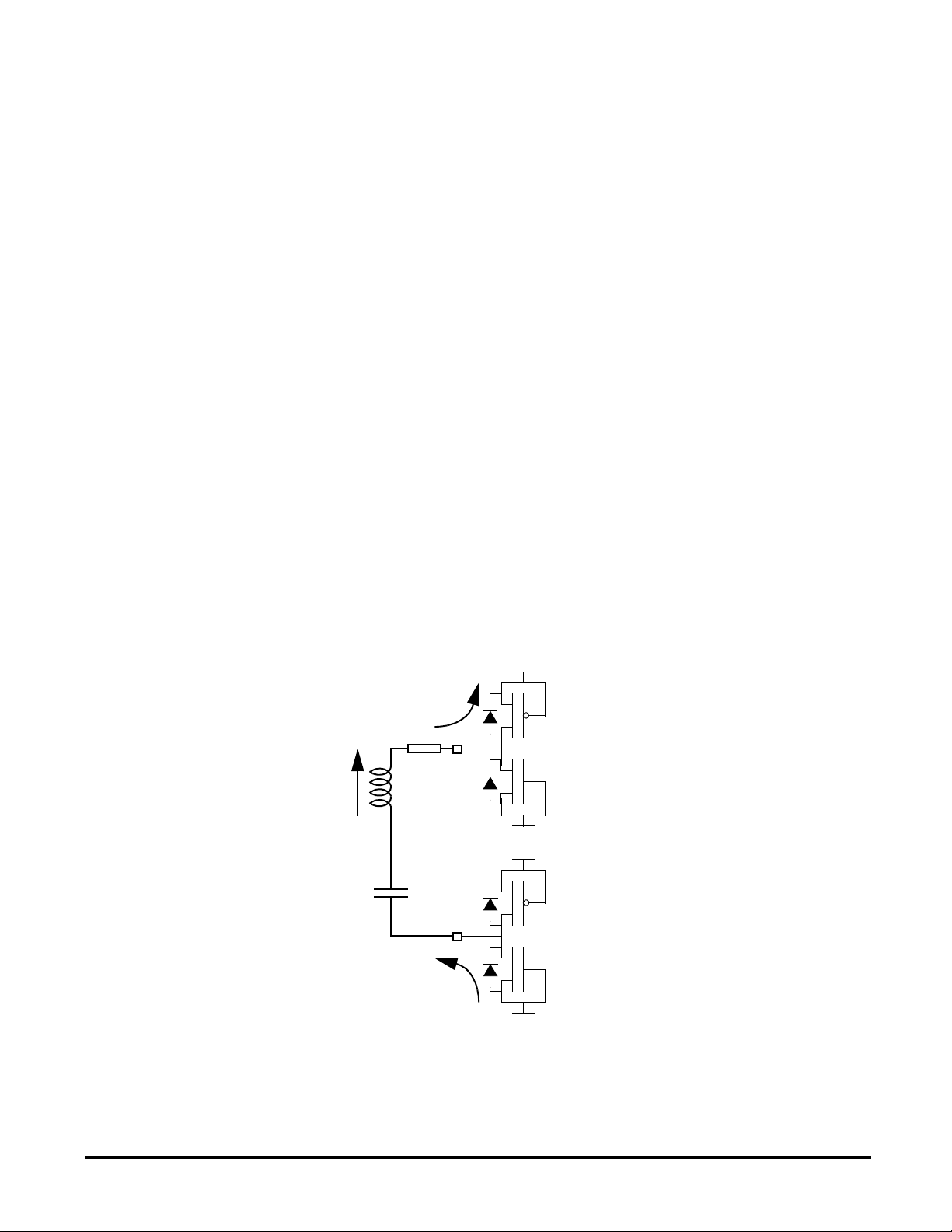
Write function
Whatever the selected configuration (see
page 9), the write function is achieved by
switching on/off the output drivers TD1/2.
Once the drivers have been set in high
impedance, the load current flows alternatively
Figure 3 : Current flow when the buffers are switched off
VDD
R
A
TD1
I
LOAD
L
A
R
1
C
A
TD2
VDD
© Motorola, Inc., 2002.
MOTOROLA SEMICONDUCTORS PRODUCTS
6
revision 4.8, 5 February 2002
Page 7
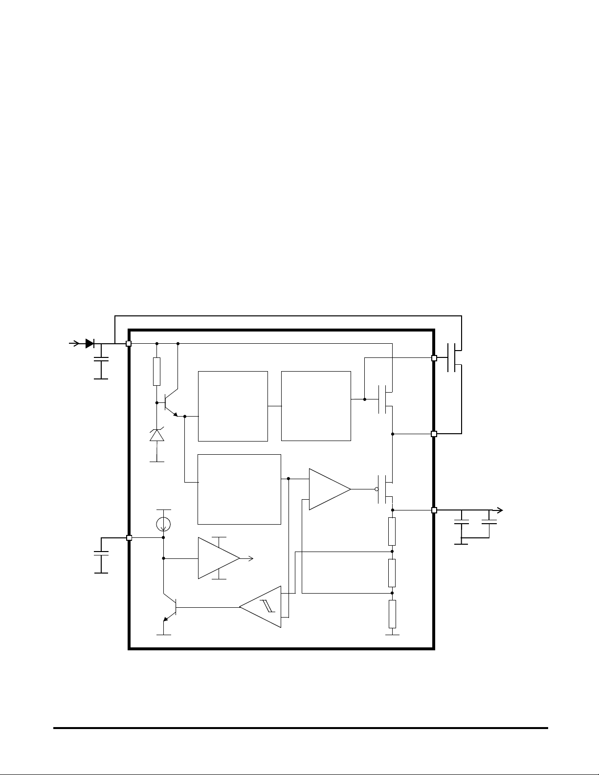
VOLTAGE REGULATOR
MC33690
The low dropout voltage regulator provides a
regulated 5V supply for the internal circuitry. It
can also supply external peripherals or sensors.
The input supply voltage ranges from 5.5V to
over 40V.
This voltage regulator uses a series combination
of high voltage LDMOS and low voltage PMOS
transistors to provide regulation. An external low
ESR capacitor is required for the regulator
stability.
The maximum average current is limited by the
power dissipation capability of the SO 20
package.
This limitation can be overcome by connecting
an external N channel MOS in parallel with the
Figure 4 : Voltage regulator block diagram
VBAT
C
1
VSUP
internal LDMOS. The threshold voltage of this
transistor must be lower than the one of the
internal LDMOS (1.95V typ.) in order to prevent
the current from flowing into the LDMOS. Its
breakdown voltage must be higher than the
maximum supply voltage.
A low voltage reset function monitors the VDD
output. An internal 10µA pull-up current source
allows, when an external capacitor is connected
between LVR and GND, to generate delays at
power up (5ms typ. with C
Reset
=22nF) .
The LVR pin is also the input generating the
internal reset signal. Applying a logic low level on
this pin resets the circuit :
- all the internal flip flops are reset,
- the drivers TD1/2 are switched on.
GATE
C
Reset
LVR
VDD
10µA
1MHz oscillator
Voltage reference
and biasing
generator
VDD
reset
Comparator
Charge pump
-
+
N channel
LDMOS
SOURCE
-
+
P channel
MOS
VDD
C
2
10µF
C
3
100nF
VDD
© Motorola, Inc., 2002.
MOTOROLA SEMICONDUCTORS PRODUCTS
7
revision 4.8, 5 February 2002
Page 8
ISO 9141 PHYSICAL INTERFACE
MC33690
This interface module is fully compatible with
the ISO 9141 norm describing the diagnosis line.
It includes one transmitter (pin K) and 2 receivers
(pins K and AM).
The input stages consist of high voltage CMOS
triggers. The thresholds are ratiometric to VSUP.
A ground referenced current source (2.5µA typ.)
pulls down the input when unconnected.
When a negative voltage is applied on the K or
AM lines, the input current is internally limited by
a 2k
Ω resistor (typ.) in series with a diode.
A current limitation allows the transmitter to drive
Figure 5 : ISO 9141interface
AM data
any capacitive load and protects against short
circuit to the battery voltage. An overtemperature
protection shuts the driver down when the
junction temperature exceeds 150°C (typ). Once
shut down by the overtemperature protection,
the driver can be switched on again :
- if the junction temperature has decreased
below the threshold,
- and by applying an off/on command, coming
either from the demodulator in configurations A
and B or directly applied on the input Tx in
configuration C (see pin K status in table 1 page
9).
The electromagnetic emission is reduced thanks
to the voltage slew rate control (5V/µs typ.).
VDD
2kΩ
VSUP
L line
AM
From configuration controller
VDD
Rx
From configuration controller
Tag Reader module output
VDD
Tx
VSUP
Over temperature
detector
Command
Current limitation
GND
GND
2.5µA
2.5µA
GND
2kΩ
VBAT
GND
K line
K
© Motorola, Inc., 2002.
MOTOROLA SEMICONDUCTORS PRODUCTS
8
revision 4.8, 5 February 2002
Page 9

MC33690
COMMUNICATION MODES DESCRIPTION
The STARC offers 3 different communication
modes. Therefore it can be used as a standalone
circuit connected to an Electronic Control Unit
Table 1. Communication modes description
Configuration
Configuration
pins
Type Bus type Name Mode1 Mode2
Standalone
Direct
connection
to a MCU
1 wire
(VBAT)
2 wires
(VBAT)
2 wires
(VDD)
A00
B01
C1
(ECU) through a bus line or it can be directly
connected to a microcontroller in case of a single
board architecture.
Pin status
& function description
K output/input :
- demodulator output,
- amplitude modulation input
- shutdown/wake-up
AM must be connected to VSUP
DOUT forces a low level
K output :
- demodulator output
AM input :
- amplitude modulation input,
- shutdown/wake-up
DOUT forces a low level
DOUT output :
- demodulator output
AM input :
x
- amplitude modulation input
MODE2 input :
- shutdown/wake-up
K output/input (standalone ISO 9141 inter-
1
face) :
- driven by Tx and monitored by Rx
K input (standalone ISO 9141 interface) :
0
- monitored by Rx
-Tx disabled
© Motorola, Inc., 2002.
MOTOROLA SEMICONDUCTORS PRODUCTS
9
revision 4.8, 5 February 2002
Page 10

MC33690
STANDALONE CONFIGURATION WITH ONE WIRE BUS
When a low level is applied on pins MODE1
and MODE2, the circuit is in configuration A
(standalone single wire bus configuration, see
figure 13 page 18).
After power on, the circuit is set into read mode.
The demodulator output is directly routed to the
ISO 9141 interface output K.
The circuit can be set into write mode at anytime
by violation of all possible patterns on the single
wire bus during more than 1ms. Then the K line
achieves the amplitude modulation by switching
on/off both antenna drivers.
After 1ms of inactivity at the end of the challenge
phase (bus in idle recessive one state), the circuit
is set back into read mode.
Figure 6 : Mode access description in one wire bus configuration
Read to write mode :
K line
read mode
Write to read mode :
K line
write mode
Write to standby mode :
K line
write mode
Standby mode to read mode :
T0 ≤ t < T0’+T1’ 1 0 0 01 1
t ≥T
0
t ≥ T
1
The circuit can be put into standby mode by
forcing the K line at zero during more than 2 ms
after entering the write mode. Once the K line is
released, the circuit sends an acknowledge pulse
before entering into standby mode.
In standby mode, the oscillator and most of the
internal biasing currents are switched off.
Therefore, the functions (tag reader, ISO 9141
driver) are inactive except the voltage regulator
and the ISO 9141 receiver on pin K. The driver
output TD1 forces a low level and TD2 a high
level. A rising edge on K wakes up the circuit.
After completion of the wake-up sequence, the
circuit is automatically set in read mode.
In configuration A, DOUT and Rx outputs always
force a low level, Tx is disabled.
write mode
read mode
T
2
acknowledge
T
2
standby mode
K line
reset
standby mode read mode
wake-up sequence
Figure 7 : Configuration A state diagram
T0 ≤ K line low
write
read
T0 ≤ K line high
TD1/2 off
K line low
T1 ≤ K line low
K line high < T
write
TD1/2
switching
’
0
wake up
K
standby
© Motorola, Inc., 2002.
MOTOROLA SEMICONDUCTORS PRODUCTS
10
revision 4.8, 5 February 2002
Page 11

Timing definitions for a 8MHz crystal:
- T
is crystal oscillator period (125 ns typ.)
ref
- T
=8064.T
0
= 1.008ms typ.
ref
MC33690
’=7932.T
- T
0
- T
=16256.T
1
- T
’=16128.T
1
=4096.T
- T
2
T
is the minimum time required to guarantee
0
= 0.992ms typ.
ref
= 2.032ms typ.
ref
= 2.016ms typ.
ref
, = 512µs typ.
ref
that the device toggles from read to write (or from
write to read). But indeed, the STARC may toggle
from read to write (or from write to read) between
T
and T0’.
0
is the minimum time required to guarantee
T
1
that the device toggles from write to standby. But
indeed, the STARC may toggle in standby
between T
and T1’.
1
© Motorola, Inc., 2002.
MOTOROLA SEMICONDUCTORS PRODUCTS
11
revision 4.8, 5 February 2002
Page 12

MC33690
STANDALONE CONFIGURATION WITH TWO WIRES BUS
When a low level is applied on MODE1 and a
high level on MODE2, the circuit is in
configuration B (standalone 2 wires bus
configuration, see figure 14 page 19).
The K pin is set as an output sending the
demodulated data.
The AM pin is set as a VSUP referenced input pin
receiving the amplitude modulation and the
shutdown/wake-up commands. Forcing high and
low levels on AM achieves the amplitude
modulation by switching on/off both antenna
drivers. Meanwhile, this amplitude modulation
can be monitored on the K output. This allows
antenna short and open circuit diagnosis.
The circuit can be put into standby mode by
Figure 8 : Modes access description in two wires bus configuration
Read & write sequences :
AM line
K line
Entering into st
AM line
K line
andby mode :
t ≥ T1
data read
T1
drivers on
acknowledge
T2 T2
forcing the AM line at zero during more than 2
ms. The circuit sends an acknowledge pulse
before entering into standby mode
In standby mode, the oscillator and most of the
internal biasing currents are switched off.
Therefore, the functions (tag reader, ISO 9141
driver) are inactive except the voltage regulator
and the ISO 9141 receiver on pin AM. The driver
output TD1 forces a low level and TD2 a high
level. A rising edge on AM wakes up the circuit.
After completion of the wake-up sequence, the
circuit is automatically set in read mode.
In configuration B, DOUT and Rx outputs always
force a low level, Tx is disabled.
drivers off
data write modulation
1 0 0 01 1
data write
1 0 0 01 1
AM line monitoring
standby mode
Coming out of standby mode :
AM line
standby mode
K line
wake-up sequence
Figure 9 : Configuration B state diagram
reset
AM line high
wake up
AM
TD1/2
switching
AM line high
AM line low
AM line low
T1 ≤ AM line low
standby
data read
TD1/2 off
© Motorola, Inc., 2002.
MOTOROLA SEMICONDUCTORS PRODUCTS
12
revision 4.8, 5 February 2002
Page 13

MC33690
DIRECT CONNECTION TO A MICROCONTROLLER CONFIGURATION
When a high level is applied on MODE1, the
circuit is in configuration C (direct connection to
a microcontroller configuration, see figure 15
page 19).
The demodulated data are sent through DOUT.
The AM pin is set as a VDD referenced input pin
receiving the AM command. Forcing high and
low levels on AM achieves the amplitude
modulation by switching on/off both antenna
drivers. Meanwhile, this amplitude modulation
can be monitored on DOUT. This allows antenna
short and open circuit diagnosis.
The circuit can be put into standby mode by
applying a low level on the MODE2 pin.
In standby mode, the oscillator and most of the
internal biasing currents are switched off.
Therefore, the functions (tag reader, ISO 9141
interface) are inactive except the voltage
Figure 10 : Configuration C state diagram
reset
TD1/2
switching
regulator. The driver outputs TD1 and TD2 are
frozen in their state (high or low level) before
entering into standby mode. DOUT forces a low
level.
The ISO 9141 interface K is standalone and can
be directly controlled by the input pin Tx and
monitored by the output Rx.
Applying a logic high level on Tx switches the
output driver K on (dominant zero state when an
external pull-up resistor is connected between K
and VBAT). Applying a logic low level turns the
driver off (one recessive state).
Rx monitors the voltage at the K pin. When the
voltage is below the low threshold voltage, Rx
forces a logic low level. When the voltage is
above the high threshold voltage, Rx forces a
logic high level.
In standby mode, Tx is disabled and Rx output
monitors the voltage at the K pin.
AM low
AM high
wake up
mode2 high
AM high
AM low
mode2 low
standby
TD1/2 off
mode2 low
© Motorola, Inc., 2002.
MOTOROLA SEMICONDUCTORS PRODUCTS
13
revision 4.8, 5 February 2002
Page 14

ELECTRICAL CHARACTERISTICS
MC33690
Typical values reflect average measurements at V
=12V and TJ=25°C.
SUP
SUPPLY CURRENT
6V ≤ V
Pin VSUP
9.1 Standby mode current I
9.2 Operating mode current I
1. Circuit in configuration C, no current sunk from VDD, drivers TD1/2 switched off, Tx forced to low.
≤ 16V, VSS = 0V, TJ = –40°C to +125°C, unless otherwise noted
SUP
Parameter
Symbol
SUP1
SUP2
Test Conditions
& Comments
See note
1
Min Typ Max Unit
- 300 500 µA
-1.52.5mA
VOLTAGE REGULATOR
6V ≤ V
Pins VSUP & VDD
1.1 Output Voltage (5.5V ≤ V
1.3 Total Output Current I
1.5 Load Regulation V
1.9 Output Voltage (5.5V ≤ V
1.11 Total Output Current I
1.6 Load Regulation V
1.4 Line Regulation (6V ≤ V
1. The stability is ensured with a decoupling capacitor between VDD and VSS : C
2. The current capability can be increased up to 150mA by using an external N channel MOS transistor (see figure 1 page 2). The main
characteristics for choosing this component are : VT < 1.8V and BVDSS > 40V.
≤ 16V, VSS = 0V, TJ = –40°C to +125°C, unless otherwise noted
SUP
Parameter
≤ 40V) V
SUP
≤ 40V) V
SUP
≤ 16V) V
SUP
Symbol
VDD1 Without external MOS transistor
VDD1
LoadReg1
VDD2
VDD2
LoadReg2
LineReg
Test Conditions
& Comments
I
≤ 50mA
OUT
Without external MOS transistor
1 to 50mA I
With external MOS transistor,
see notes
I
OUT
With external MOS transistor
1 to 150mA I
I
OUT
change
OUT
1
and
≤ 150mA
change
OUT
= 1mA -15 -1 - mV
≥ 10µF with ESR ≤ 3Ω.
OUT
Min Typ Max Unit
4.75 5.0 5.25 V
--50mA
-2060mV
2
4.7 5.0 5.3 V
--150mA
-65150mV
Typ e
Typ e
© Motorola, Inc., 2002.
MOTOROLA SEMICONDUCTORS PRODUCTS
14
revision 4.8, 5 February 2002
Page 15

LOW VOLTAGE RESET
MC33690
6V ≤ V
Pin LVR
1.6 Low Voltage Reset Low Threshold V
1.7 Low Voltage Reset Hysteresis V
1.12 Pull-up Current I
1.13 Output Resistance in reset condition R
1.14 Input Low Voltage V
1.15 Input High Voltage V
1. As the voltage regulator and the low voltage reset are using the same internal voltage reference, it is ensured that the low voltage reset
will only occur when the voltage regulator is out of regulation.
≤ 16V, VSS = 0V, TJ = –40°C to +125°C, unless otherwise noted
SUP
Parameter
Symbol
LVR ON
LVR H
LVRUP
LVR
ILLVR
IHLVR
Test Conditions
& Comments
See note 1 and figure 11
V
= 2.5V
LVR
V
= 2.5V
LVR
Min Typ Max Unit
4.14.354.6 V
50 100 150 mV
51015µA
200 370 500 Ω
0-
0.7 x
V
DD
0.3 x
V
DD
-VDDV
V
Figure 11 : Low voltage reset waveform
VDD
V
V
LVRON
LVRON
+ V
LVRH
LVR
Typ e
OSCILLATOR
6V ≤ V
Pins XTAL1, XTAL2
8.0 Input Capacitance C
8.1 Voltage gain V
8.3 Clock input level V
1. This level ensures the circuit operation with a 8MHz clock. It is applied through a capacitive coupling. A 1MΩ resistor connected between
XTAL1 and XTAL2 biases the oscillator input.
≤ 16V, VSS = 0V, TJ = –40°C to +125°C, unless otherwise noted
SUP
Characteristic
/ V
XTAL2
XTAL1
Symbol
XTAL1
A
OSC
XTAL1
Test Condition
& Comments
V
= 2.5V - 5 - pF
XTAL1
V
= 2.5V - 25 - -
XTAL1
See note
1
Min Typ Max Unit
1.5 - V
DD
Vpp
Typ e
© Motorola, Inc., 2002.
MOTOROLA SEMICONDUCTORS PRODUCTS
15
revision 4.8, 5 February 2002
Page 16

TAG READER
MC33690
6V ≤ V
≤ 16V, VSS = 0V, TJ = –40°C to +125°C, unless otherwise noted
SUP
Parameter
Symbol
DEMODULATOR (pin RD)
2.0 Input Voltage Range V
2.2 Input Modulation Frequency F
2.3 Demodulator Sensitivity V
2.31 Demodulator Sensitivity V
2.4 Demodulation Delay t
2.5 After Write Pulse Settling Time t
INRD
MOD
SENSE1
SENSE2
Demod
Settling1
See figure 12 and note
See figure 12 and note 1 - 7 30 mV
see note
Recovery Time after wake-up or reset
2.6
from clock stable to demodulator valid
t
Settling2
output
DRIVERS (pins TD1, TD2)
Output Carrier Frequency to Crystal
3.5
Frequency Ratio
3.0 Turn on/off Delay t
3.1 Driver1/2 Low Side Out. Resistance R
3.2 Driver1/2 High Side Out. Resistance R
R
FTD/
FXTAL
on/off
TDL
TDH
1. The sensitivity is measured in the following application conditions : I
modulation F
2. Not including the delay due to the slew rate of the K output.
MOD=FTD1
3. Clock stable condition implies V
/32.
meets the specification (see page 15).
XTAL1
Test Conditions
& Comments
Min Typ Max Unit
345V
0.5 4 8 kHz
6.5V ≤ V
6V ≤ V
SUP
SUP
≤ 16V
< 6.5V
1
-515mV
See figure 12
Configuration C
2
for configurations A
-7.510µs
and B
- 394 400 µs
See note
3
- 646 700 µs
-64--
- - 250 ns
I
= 150mA DC - 2.4 4 Ω
LOAD
I
= -150mA DC - 2.1 4 Ω
LOAD
ANTENNA
= 50mA peak, VRD = 4V peak, C
= 10nF, square wave
EXT
Type
Figure 12 : Demodulator parameters definition
V
RD
Demodulator
output (K or DOUT)
V
SENSE
t
Demod
© Motorola, Inc., 2002.
MOTOROLA SEMICONDUCTORS PRODUCTS
16
revision 4.8, 5 February 2002
Page 17

ISO 9141 INTERFACE
MC33690
6V ≤ V
≤ 16V, VSS = 0V, TJ = –40°C to +125°C, unless otherwise noted
SUP
Parameter
Symbol
Test Conditions
& Comments
Min Typ Max Unit
Receiver (pins K & AM)
4.0 Input Low Voltage V
4.1 Input High Voltage V
4.2 Input Hysteresis Voltage V
4.3 Biasi ng Cur re nt I
4.31 Input C ur rent I
IL
IH
HY1
B
BM
-3 -
0.65 x
V
SUP
0.40.651.3 V
0V ≤ VIN ≤ 16V 1 3 5 µA
-3 ≤ VIN < 0-2-1-mA
0.3 x
V
SUP
-40V
4.4 K to Rx delay tdkrx 2 10 µs
Driver (pin K)
5.0 Output Falling Edge Slew Rate SR
5.1 Output Rising Edge Slew Rate SR
5.2 Rise Fall Slew Rates Symmetry
SR
5.3 Output Low Voltage V
Input Current
5.4
(driver switched on or off)
5.5 Current Limitation Threshold I
5.6 Thermal Shutdown Threshold TH
1. Calculated from 20% to 80% of the output swing.
F
R
SYME-
TRY
OLK
I
IK
L
SDWN
R
= 510Ω,
Pull-up
see note
I
LOAD
1
= 25mA - 1.1 1.4 V
-3V ≤ VIN ≤ 0V -2 - 0 mA
0V ≤ VIN ≤ 40V 35 50 65 mA
3.5 5 6.5 V/µs
3.5 5 6.5 V/µs
-1 0 1 V/µs
130 150 170 °C
Typ e
V
DIGITAL I/O
6V ≤ V
INPUT (pins MODE1, MODE2, AM, TX)
6.0 Input Low Voltage V
6.1 Input High Voltage V
6.2 Input Hysteresis Voltage
OUTPUT (pins DOUT,RX)
7.0 Output Low Voltage V
7.1 Output High Voltage V
7.2 Fall/Rise Time t
1. Calculated from 10% to 90% of the output swing.
≤ 16V, VSS = 0V, TJ = –40°C to +125°C, unless otherwise noted
SUP
Characteristic
Symbol
ILD
IHD
V
HD
OL
OH
F/R
Test Condition
& Comments
I
= 500uA 0 0.5
LOAD
I
= -500uA
LOAD
C
=10pF, see note
LOAD
Min Typ Max Unit
0-
0.7 x
V
DD
.24 .7 1 V
0.8 x
V
1
DD
- - 150 ns
-VDDV
4.6 V
0.3 x
V
DD
0.2 x
V
DD
DD
Typ e
V
V
V
© Motorola, Inc., 2002.
MOTOROLA SEMICONDUCTORS PRODUCTS
17
revision 4.8, 5 February 2002
Page 18

APPLICATION SCHEMES
Figure 13 : Standalone configuration with one wire bus
VBAT
C
1
NC
GATE
NC
SOURCE
MC33690
VSUP
LVR
XTAL1
XTAL2
MODE1
MODE2
NC
DOUT
AM
K
NC
1MΩ
VSUP
8.2pF
8MHz
8.2pF
VBAT
510Ω
VSS
L
C
C
10µF
A
A
R
C
2
1
C
EXT
3
100nF
R
R
2
A
NC
VDD
VSS
TD1
RD
TD2
CEXT
10nF
AGND
STARC
Tx
Rx
If no external MOS transistor is necessary to increase the voltage regulator current capability, the pins GATE
and SOURCE must be left unconnected.
In this configuration, the outputs Rx and DOUT force a low level.
C
is not required for the STARC functionality and only acts as a reservoir of energy.
1
To preserve the demodulator sensitivity,
C
and R2 should be connected to AGND, and VSS connected to
EXT
AGND using a low resistance path.
© Motorola, Inc., 2002.
MOTOROLA SEMICONDUCTORS PRODUCTS
18
revision 4.8, 5 February 2002
Page 19

VBAT
MC33690
Figure 14 : Standalone configuration with two wires bus
C
1
NC
GATE
NC
SOURCE
VSUP
LVR
XTAL1
XTAL2
MODE1
MODE2
NC
1MΩ
8.2pF
8MHz
8.2pF
VDD
VBAT
VSS
L
A
C
A
C
10µF
R
1
C
2
3
VDD
100nF
VSS
R
A
TD1
R
2
RD
STARC
TD2
NC
C
EXT
CEXT
10nF
AGND
Tx
DOUT
K
AM
510Ω
NC
Rx
If no external MOS transistor is necessary to increase the voltage regulator current capability, the pins GATE
and SOURCE must be left unconnected.
C
is not required for the STARC functionality and only acts as a reservoir of energy.
1
To preserve the demodulator sensitivity,
AGND using a low resistance path.
© Motorola, Inc., 2002.
C
and R2 should be connected to AGND, and VSS connected to
EXT
MOTOROLA SEMICONDUCTORS PRODUCTS
19
revision 4.8, 5 February 2002
Page 20

VBAT
To microcontroller
power supply pin
C
VSS
L
C
10uF
A
A
R
MC33690
Figure 15 : Direct connection to a microcontroller
C
1
NC
GATE
NC
SOURCE
C
2
3
VDD
100nF
VSS
R
A
TD1
1
R
RD
2
STARC
VSUP
LVR
XTAL1
XTAL2
MODE1
1MΩ
VDD
To microcontroller
port/reset pin
8.2pF
8MHz
8.2pF
TD2
MODE2
To microcontroller
port
DOUT
AM
K
VBAT
510Ω
To microcontroller
port
C
EXT
CEXT
10nF
AGND
Tx
Rx
If no external MOS transistor is necessary to increase the voltage regulator current capability, the pins GATE
and SOURCE must be left unconnected.
is not required for the STARC functionality and only acts as a reservoir of energy.
C
1
To preserve the demodulator sensitivity,
AGND using a low resistance path.
C
and R2 should be connected to AGND, and VSS connected to
EXT
© Motorola, Inc., 2002.
MOTOROLA SEMICONDUCTORS PRODUCTS
20
revision 4.8, 5 February 2002
Page 21

MC33690
Notes
© Motorola, Inc., 2002.
MOTOROLA SEMICONDUCTORS PRODUCTS
21
revision 4.8, 5 February 2002
Page 22

MC33690
Notes
© Motorola, Inc., 2002.
MOTOROLA SEMICONDUCTORS PRODUCTS
22
revision 4.8, 5 February 2002
Page 23

MC33690
Notes
© Motorola, Inc., 2002.
MOTOROLA SEMICONDUCTORS PRODUCTS
23
revision 4.8, 5 February 2002
Page 24

MC33690
Motorola reserves the right to make changes without further notice to any products herein. Motorola makes no warranty, representation or guarantee regarding
the suitability of its products for any particular purpose, nor does Motorola assume any liability arising out of the application or use of any product or circuit, and
specifically disclaims any and all liability, including without limitation consequential or incidental damages. “Typical” parameters which may be provided in Motorola
data sheets and/or specifications can and do vary in different applications and actual performance may vary over time. All operating parameters, including
“Typicals” must be validated for each customer application by customer ’s technical experts. Motorola does not convey any license under its patent rights nor the
rights of others. Motorola products are not designed, intended, or authorized for use as components in systems intended for surgical implant into the body, or
other applications int ended to support or sustain life, or for any other application in which the failure of t he Motorola product could create a situation where personal
injury or death may occur. Should Buyer purchase or use Motorola products for any such unintended or unauthorized application, Buyer shall indemnify and hold
Motorola and its officers, employees, subsidiaries, affiliates, and distributors harmless against all claims, costs, damages, and expenses, and reasonable attorney
fees arising out of, directly or indirectly, any claim of personal injury or death associated with such unintended or unauthorized use, even if such claim alleges that
Motorola was negligent regarding the design or manufacture of the part. Motorola and the Stylized M Logo are registered in the U.S. Patent and Trademark Office.
Motorola, Inc. is an Equal Opportunity/Affirmative Action Employer. All other product or service names are the property of their respective owners.
© Motorola, Inc. 2002
HOW TO REACH US:
USA/EUROPE/LOCATIONS NOT LISTED: Motorola Literature Distribution: P.O. Box 5405, Denver, Colorado 80217.
1-303-675-2140 or 1-800-441-2447
JAPAN: Motorola Japan Ltd.; SPS, Technical Information Center, 3-20-1 Minami-Azabu. Minato-ku, Tokyo 106-8573 Japan.
81-3-3440-3569
ASIA/PACIFIC:
Motorola Semiconductors H.K. Ltd.; Silicon Harbour Centre, 2 Dai King Street, Tai Po Industrial Estate, Tao Po, N.T.,
Hong Kong. 852-26668334
TECHNICAL INFORMATION CENTER:
HOME PAGE:
http://motorola.com/semiconductors/
1-800-521-6274
MC33690/D
 Loading...